Note: Descriptions are shown in the official language in which they were submitted.
FJ-7022
- 1 1 3 3 8 7 4 1
DATA COMMUNICATION SYSTEM HAVING
CHANNEL SWITCHING MEANS
RACK~ROUND OF THE INVENTION
1. Field of the Invention
The present invention relates to a data
communication system having a channel switching means,
for example, a radio data communication system provided
with channel switching equipment between a main channel
and a protection channel.
2. Description of the Related Art
Usually, a channel switching means which is
employed in a data communication system uses both a main
channel and protection channel. That is, when the
transmission quality of the main channel deteriorates,
and accordingly a data error rate increases, a trans-
mitting terminal station automatically switches the
transmission line from the main channel, which is
transmitting data to a receiving terminal station, tothe protection channel, which is transmitting auxiliary
data thereto. To cope with this, the receiving terminal
station selects data received via the protection channel
instead of the main channel, and outputs the same as
main channel data.
The above-mentioned channel switching can be
performed without even an instantaneous interruption in
the flow of data if the above-mentioned transmission
quality deteriorates slowly. However, if the trans-
mission quality deteriorates quickly, it is very liableto result in an instantaneous interruption in the flow
of data. Thus, in the field of data communication
systems, it has been hoped to prevent such an instanta-
3~ neous interruption in data flow caused by channelswitching when rapid deterioration of the transmission
quality occurs due to, for example, sudden fading.
In the prior art, as will be exemplified in
-
1 33874 1
detail hereinafter, there is an inevitable loss of data during
the short transition period when switching from the main
channel to the protection channel. Thus, the prior art channel
switching means used in data communication systems produces a
problem in that there is a high probability of a data error
occurring when there is a rapid deterioration in transmission
quality.
SUMMARY OF THE INVENTION
In accordance with an embodiment of the present invention
lo there is provided a data communication system for sending data
over a main channel and a protection channel, the system com-
prising: transmitter means for providing the data to the main
channel, for delaying the data to produce first delayed data
and for providing the first delayed data to the protection
channel, the transmitter means including: channel switching
means for selectively providing the first delayed data to the
protection channel when receiving a command signal that
indicates a transmission fault on the main channel; receiver
means for receiving the data from the main channel and the
first delayed data from the protection channel, the receiver
means including: delay means for delaying the data received
from the transmitter means via the main channel to produce
second delayed data, and detection means for detecting the
transmission fault and, in response, providing the command
signal; and wherein a first delay time of the first delayed
data is substantially the same as a second delay time of the
second delayed data, each of the first and second delay times
comprising a data-stoppage time between occurrence of the
transmission fault and the detection of the transmission fault,
a first propagation delay time indicative of a length of time
the command signal propagates from the detection means to the
channel switching means, a second propagation delay time
indicative of a length of time the first delayed data
propagates through the protection channel to the receiver
1 33874 1
- 2a -
means, and a period of time required to confirm receipt by the
receiver means of the first delayed data and to switch an
output of the data communication system from the second delayed
data to the first delayed data.
In accordance with another embodiment of the present
invention there is provided a data communication system for
sending data over a main channel and a protection channel from
a transmitter to a receiver, the transmitter comprising: first
transmission means for providing the data to the main channel;
second transmission means for delaying the data to produce
first delayed data and for providing the first delayed data to
the protection channel, the second transmission means includ-
ing: channel switching means for selectively providing the
first delayed data to the protection channel when receiving a
command signal that indicates a transmission fault on the main
channel; the receiver comprising: first receiver means for
receiving the data from the main channel; delay means for
delaying the data received by the first receiver means to
produce second delayed data; second receiver means for
receiving the first delayed data from the protection channel;
and detection means for detecting a transmission fault based
on the data from the main channel and providing the command
signal; and wherein a first delay time of the first delayed
data is substantially the same as a second delay time of the
second delayed data, each of the first and second delay times
comprising a data-stoppage time between occurrence of the
transmission fault and the detection of the transmission fault,
a first propagation delay time indicative of a length of time
the command signal propagates from the detection means to the
channel switching means, a second propagation delay time
indicative of length of time the second delayed data propagates
through the protection channel to the second receiver means,
and a period of time required to confirm receipt by the second
receiver means of the first delayed data and to switch an
~,
-
1 33874 1
- 2b -
output of the data communication system from the second delayed
data to the first delayed data.
In accordance with yet another embodiment of the present
invention there is provided a data communication system for
sending information data from an input terminal over a main
channel and a protection channel to an output terminal, the
system comprising: transmitter means, receiving the information
data from the input terminal, for providing the information
data to the main channel regardless of whether a transmission
fault exists on the main channel, for delaying the information
data to produce first delayed data and for outputting the first
delayed data, the transmitter means comprising: first channel
switching means for selectively enabling transmission of the
first delayed data output from the transmitter means to the
protection channel in response to a command signal indicative
of a transmission fault on the main channel; and receiver means
for receiving the information data from the main channel, and
for receiving the first delayed data when the fault exists on
the main channel, the receiver means comprising: detection
means for determining whether the transmission fault exists on
the main channel and, in response, providing the command
signal, delay means for delaying the information data trans-
mitted over the main channel to produce second delayed data
after the determination by the detection means; and second
channel switching means alternately enabling transmission of
one of the first and second delayed data in dependence upon the
determination of the detection means.
In accordance with a still further embodiment of the
present invention there is provided a data communication system
for sending information data from an input terminal over a main
channel and a protection channel to an output terminal, the
system comprising: transmitter means, receiving the information
data from the input terminal, for providing the information
data to the main channel, and selectively providing the same
~j
1 338741
information data delayed a predetermined time period as first
delayed data to the protection channel in response to a command
signal indicative of a transmission fault on the main channel;
and receiver means for receiving the information data from the
main channel, and for receiving the first delayed data when the
fault exists on the main channel, the receiver means compris-
ing: detection means for determining whether the transmission
fault exists on the main channel and, in response, providing
the command signal; delay means for delaying, after the
determination by the detection means, the information data
transmitted over the main channel to produce second delayed
data; and second channel switching means for alternately
enabling transmission of one of the first and second delayed
data to the output terminal in dependence upon the deter-
mination of the detection means.
BRIEF DESCRIPTION OF THE DRAWINGS
The above features of the present invention will be more
apparent from the following description of the preferred
embodiments with reference to the accompanying drawings,
wherein:
Fig. 1 is a general block diagram of a prior art data
communication system;
Fig. 2 depicts timing charts showing one example of a
channel switching procedure when a fault occurs in the system
of Fig. 1;
Fig. 3 is a principle block diagram of a data communi-
cation system according to the present invention;
Fig. 4 is a more detailed block diagram of the data
i ~
1 33874 ~
communication system shown in Fig. 3.
Fig. 5 shows timing charts for illustrating one
example of a channel switching procedure when a fault
occurs in the system of Fig. 3;
Fig. 6 illustrates a detailed example of a trans-
mitting unit;
Fig. 7 illustrates a detailed example of a
receiving unit;
Fig. 8 illustrates a detailed example of a
receiving and retransmitting unit;
Fig. 9 illustrates a detailed example of a
synchronous switch circuit;
Fig. 10 depicts timing charts for explaining the
operation of the circuit in Fig. 9;
Fig. 11 illustrates a detailed example of a
transmitter side delay means;
Fig. 12 illustrates a detailed example of a
receiver side delay means which is provided with a
detection means;
Fig. 13 illustrates a detailed example of a
receiving channel switch circuit;
Fig. 14 illustrates a detailed example of receiving
and transmitting control circuits;
Fig. 15 illustrates a detailed example of a trans-
mitting channel switch unit;
Fig. 16 is a specific block diagram of a test pulse
generator; and
Fig. 17 is a specific block diagram of a test pulse
detector.
DESCRIPTION OF THE PREFERRED EMBODIMENTS
Before describing the embodiments of the present
invention, the related art and the disadvantages therein
will be described with reference to the related figures.
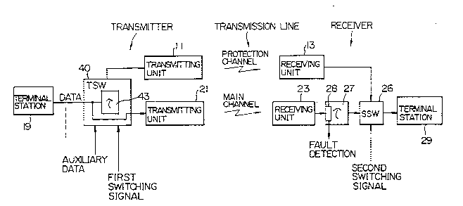
Figure 1 is a general block diagram of a prior art
data communication system, and Figure 2 depicts timing
charts for showing one example of a channel switching
procedure when a fault occurs in the system of Fig. 1.
-- 4
1 338741
The operation of the channel switching performed in the
data communication system of Fig. 1 will be clarified
with reference to the timing charts shown in Fig. 2.
The numerals in parentheses in the leftmost column in
Fig. 2 indicate that the respective timing charts
correspond to the portions referenced by the numerals
enclosed in quotation marks " " in Fig. 1. The fol-
lowing explanation will use as an example a system
having a single protection channel and a single main
channel. In actuality, a plurality of channels exist,
in the form of, for example, frequency division
multiplex communication (FDM), used in the main channel.
However, for the safe of simplicity only one channel is
shown (this also applied to later figures).
(A) Case where main channel and protection channel
are normal
Bipolar data is provided by a data source located
in, for example, a transmitting terminal station 19.
The data is branched in two directions by a hybrid
circuit (H) 201 which is mounted in a transmitting
channel switch unit (TSW) 20. One of the data branches
is transferred to a transmitting unit 21, and the other
is applied to a switch circuit (SW) 202, but prevented
from passing therethrough.
In the main channel transmitting unit 21, the
bipolar data is first transformed into unipolar data,
and a carrier wave is then modulated by the thus trans-
formed unipolar data. A l~cal oscillator for producing
the carrier wave is not sh~wn in the figure. Next, the
modulated carrier wave is converted upward in frequency
and energized to have enough transmission power to
radiate from the transmitter to the receiver via a
transmission line which includes a repeater or
repeaters, more specifically, via a receiving and
retransmitting unit or units 22 contained in each
repeater.
The data from the last repeater is received by a
_ - 5 - l 33 87 4l
receiving unit 23 located in the receiver, wherein the
unipolar data is provided to a synchronous switch
circuit (SSW) 24. The synchronous switch circuit (SSW)
24 transforms unipolar data to bipolar data and outputs
the bipolar data to a switch circuit 25. The switch
circuit 25 supplies the bipolar data to a receiving
terminal station 29 to reproduce the original data.
Incidentally, the synchronous switch circuit (SSW) 24 is
usually fabricated using a semiconductor integrated
circuit (IC) which is able to achieve high speed
synchronous switching from the main channel data to the
protectïon channel data. The switch circuit (RSW) 25 is
located after the switch ~ircuit (SSW) 24 to back-up the
latter switch circuit 24.
In the normal state of the main channel system, it
is theoretically not necessary to activate the protec-
tion channel system, but in practice, the protection
channel system is activated so as to always supervise
the condition of the protection channel system to
maintain the normal state thereof. For this purpose,
the protection channel system handles auxiliary data
during activation of the main channel system. The
auxiliary data is, for example, test data. The related
test pulse is generated by a test pulse generator 30 and
transmitted to a test pulse detector 33 located in the
receiver, via the switch circuit 202, a protection
channel transmitting unit 11, a receiving and retrans-
mitting unit 12, a protection channel receiving unit 13
and the receiving channel switch circuit (RSW) 25. If
the predetermined pattern of the test pulse is detected
correctly by the detector 33, it is determined that the
protection channel system is normal. In that case, the
main channel can freely be switched to the protection
channel when the transmission quality of the main
channel data deteriorates.
(B) Case where fault occurs at rePeater in main
channel system
_ - 6 - 1 33874 1
First, the original data is sent from the aforesaid
data source in the transmitting terminal station 19 to
the main channel transmitting unit 21, as shown by the
first part of row (1) in Fig. 2. The characters Tl, T2,
and so on, above row (1) denotes a time scale, where
Tl < T2 < T3 < T4, i.e., Tl occurs in time before T4.
The data from the transmitting unit 21 is transmitted,
as mentioned above, to the receiving terminal
station 29, via the transmitting channel switch unit
(TSW) 20, the main channel transmitting unit 21, the
main channel receiving and retransmitting unit 22, the
main channel receiving unit 23, the synchronous switch
circuit (SSW) 24, and the receiving channel switch
circuit (RSW) 25.
1~ Suppose now that some fault occurs at the repeater, and accordingly a stoppage of data takes place in the
main channel as shown in row (2) of Fig. 2. The
stoppage of data is detected after a time tl occurring
from the stoppage of data, as shown in row (3). The
time tl is required by a data stoppage detector in order
to detect the related data stoppage. This data stoppage
detector (not shown) is usually mounted in the
synchronous switch circuit (SSW) 24. The detection of
data stoppage is reported by the data stoppage detector
to a receiving control circuit 32, and the circuit 32
then transmits a command signal to a transmitting
control circuit 31 via another transmission line 34,
e.g., a downstream line instead of a upstream line
through which the main channel data has been transmitted
(refer to row (4)). The symbol t2 denotes the transmis-
sion time through the transmission line 34.
The transmitting control circuit 31 issues a
switching signal to the switch circuit (SW) 202 in the
transmitting channel switch unit (TSW) 20. When the
switching signal is received, the switch circuit 202
changes its status from one state to the other state.
Accordingly, the switch circuit 202 prevents the signal
- 7 - 1 3 3 8 7 4 1
from the test pulse generator 30 from passing
therethrough, while allowing the signal from the hybrid
circuit (H) 201 to pass. Thus the transmitting channel
switch unit (TSW) 20 provides data, instead of the test
pulse, which is the same as the data which had been
provided to the main channel up to that point in time
and had been transferred to the protection channel
transmitting unit 11, so that the data from the
aforesaid data source is also transferred to the
receiver via the protection channel. Under these
conditions, the data is sent to both the main channel
transmitting unit 21 and the protection channel trans-
mitting unit 11. This is known as a parallel trans-
mission. The symbol t'2 (in row (6)) denotes the time
for downstream transmission of data through the trans-
mission line (protection channel). The value of t'2 is,
of course, the same as that of the upstream transmission
time t2 (refer to row (4)).
After a time t3 (refer to row (7)) occurring from
the elapse of the time t2 ~ the data starts being
applied via the protection channel to the receiving
synchronous switch circuit (SSW) 24. In this case, when
the switch (SSW) 24 detects that the data, transmitted
through the protection channel, has been received, the
related detection signal from the switch (SSW) 24 is
sent to the receiving control circuit 32 so that a
switching signal (refer to row (7)) from the control
circuit 32 can be sent to the switch circuit (SSW) 24.
This switching signal changes the status of the switch
3n circuit (SSW) 24 changes its status preventing the
unipolar output signal from the main channel receiving
unit 23, but allowing the unipolar output signal from
the protection channel receiving unit 13 to pass through
the switch circuit (SSW) 24. Thereby, the inherent main
channel data is transmitted from the transmitter to the
receiving terminal station 29 via the protection channel
system, i.e., the receiving unit 13, and also via the
- - 8 - l 3 3 8 7 4 1
switch circuit (SSW) 24 and the switch circuit (RSW) 25.
In this case, the aforesaid term t3 represents the time
required to confirm the detection of the received data
through the protection channel and to switch the switch
circuit (SSW) 24. It should be understood here that a
response signal from the transmitter via the trans-
mission line 34, and also a response signal from the
switch circuit (SSW) 24, are omitted from Fig. 2 for
brevity.
In conclusion, an undesired interruption in data
flow occurs during the time t4 (refer to row (8) in
Fig. 2). That is, there is a partial data loss causing
a data error. This is the problem occurring in the
prior art data communication system. In this case, the
interruption time t4 is expressed as follows:
t4 = t1 + t2 + t 2 + t3
Figure 3 is a principle block diagram of a data
communication system according to the present invention.
Note that items identical to those explained before are
represented by the same reference numerals or characters
(this also applies to later figures). In this figure, a
synchronous switch circuit (SSW) 26, a delay means
( r ) 27, a transmitting channel switch unit (TSW) 40 and
another delay means ( r ) 43 are newly recited items.
Among these, the SSW 26 and the TSW 40 are functionally
similar to the aforesaid SSW 24 and TSW 20, respec-
tively.
The delay means 27 delays the data in time by a
period r. The delayed data is then received from the
transmitter via the transmission line which usually
includes a plurality of repeaters (not shown in Fig. 3
but indicated in Fig. 1 by reference numerals 12 and
22). The delay means 27 is located along a signal line
through which the main channel is formed.
The transmitter contains therein another delay
means ( r ) 43. The delay means 43 delays the data in
time by a period r, said data being received from the
-- 9 1 338741
aforesaid data source which is usually located in the
transmitting terminal station 19. This data is to be
transmitted to the receiver not by way of the main
channel but by the protection channel.
The receiver contains therein a detection means 28
preferably in the delay means 27 as illustrated. The
detection means 28 detects an occurrence of a transmis-
sion fault in the main channel. The detection means 28
is located in a preceding stage relative to the delay
means 27, or in a front stage thereof.
The detection means 28 issues a fault detection
signal if a related fault takes place. The fault
detection signal induces two commands. The first
command applies a first switching signal to the trans-
mitting channel switch unit (TSW) 40 via the transmis-
sion line (shown as 34 in Fig. 1). The second command
applies a second switching signal to the synchronous
switch circuit (SSW) 26. The first switching signal
activates the transmitter side (transmitting) channel
switch unit 40 so as to transmit the original data from
the aforesaid data source to the receiver by way of the
transmitter side (transmitting) delay means 43 and
through the protection channel. While, the second
switching signal activates the receiver side (receiving)
channel switching means, i.e., the synchronous switch
circuit (SSW) 26, after a predetermined elapsed time
from the detection of the transmission fault indicated
by the fault detection signal. In this way the data
received via the protection channel overlaps with the
data delayed by the delay means (r) 27.
The delay times r caused at both the delay means 43
and 27 are set to substantially the same time. Each
delay time r is defined as the aforesaid stoppage time
(refer to "t4" in row (8) of Fig. 2) plus a predeter-
mined time margin.
General operation is as follows. When the originaldata is to be switched to the protection channel
1 33 8 74 1
-- 10 --
transmitting unit 11 by means of the switch unit
(TSW) 40, this data is delayed in time by the delay
time r. The time r is expressed as follows.
r = ti + t2 + t 2 3
The meanings of each of the symbols tl, t2 '
except for t~ , have already been explained. The symbol
t~ denotes a predetermined time margin. The remaining
terms denote, as mentioned previously, that t1 is a
fault detection time, t2 is a downstream transmission
time t'2 (= t2) is an upstream transmission time, and t3
is a switching time, and the symbol t4 (= tl + t2 + t'2
+ t3) represents a stoppage time of data flow which
would inevitably occur in usual channel switching.
The delay time r is created in the transmitter by
the delay means 43 which is mounted in the transmitting
channel switch unit (TSW) 40. To cope with this, the
aforesaid delay means 27 is introduced between the main
channel receiving unit 23 and the synchronous switching
circuit 26. When a transmission fault is detected by
the detection means 27, data is applied to both the main
channel side input and the protection channel side input
of the switch circuit 26, both blocks of data being the
same as the data which had already been delayed by the
time ( r ) before the occurrence of the related transmis-
sion fault. The aforesaid second switching signal isthen supplied to the switch circuit (SSW) 26 by the end
of the time t4 (refer to row (8) of Fig. 2). During the
time t4 the delayed data, i.e., previous data, in the
delay means 27 is maintained so that channel switching
by the switch circuit (SSW) 26 can be achieved without
stopping the data flow. It is important to understand
that this channel switching can be achieved with no loss
of data due to deterioration of the transmission quality
caused by sudden fading or even a sudden problem with
the electronic communication apparatus.
Figure 4 is a more detailed block diagram of a data
communication system shown in Fig. 3, and Figure 5
- - 11 1 338741
depicts timing charts for illustrating one example of a
channel switching procedure when a fault occurs in the
system of Fig. 3. The procedure shown Fig. 5 assumes a
case where a transmission fault has occurred due to some
trouble in the main channel receiving and retransmitting
unit 22 in the system of Fig. 4. Like the previous
Figs. 1 and 2, the numerals in parentheses in the
leftmost column in Fig. 5 indicate that the respective
timing charts correspond to the portions referenced by
the corresponding numerals given in quotation marks " "
in Fig. 4. Therefore, Figs. 4 and 5 are read in the
same manner as the previous Figs. 1 and 2. In Fig. 4,
the transmitting channel switch unit (TSW) 40 is com-
prised of the delay means 43, a hybrid circuit (H) 41
(similar to the corresponding circuit 201 in Fig. 1) and
a switch circuit (SW) 42 (similar to the corresponding
circuit 202 in Fig. 1).
It should be recognized that the operation during
the normal state of the main channel system, is
identical to the operation which has been explained with
respect to the prior art by referring to Figs. 1 and 2,
except that the received data in the receiver (Fig. 4)
according to the present invention, is always delayed by
the delay time r relative to that in the prior art
receiver shown in Fig. 1. Accordingly, the following
explanation will use as an example a case where a
transmission fault has actually taken place.
Before the occurrence of a transmission fault, the
original data is sent from the aforesaid data source in
the transmitting terminal station 19, as shown in
row (1) of Fig. 5, the structure of this data being
schematically illustrated, e.g., as shown by ... D 1 '
Do , Dl , D2 .... The original data is transferred to
the receiving terminal station 29 by way of the trans-
mitting channel switch unit (TSW) 40, the main channeltransmitting unit 21, the receiving and retransmitting
unit 22, the receiving unit 23, the receiver side delay
_ - 12 - 1338741
means 27, the synchronous switch circuit (SSW) 26, and
the receiving channel switch circuit 25.
Here, assuming that a stoppage of data occurs due
to the aforesaid transmission fault, e.g., a problem in
the receiving and retransmitting unit 22. The stoppage
of data is schematically shown in row (2) of Fig. 5,
where t2 denotes the transmission time of the data from
the transmitter to the portion "2" in the receiver. The
transmission fault, i.e., the stoppage of data, is
detected by the fault detection means 28 within the
fault detection time tl which is shown in row (3) of
Fig. 4. The related fault detection signal is sent to
the receiving control circuit 32, and the receiving
control circuit 32 issues a command to the transmitting
control circuit 31 in the transmitter via the upstream
channel of the transmission line 34. The control
circuit 31 in the transmitter then provides the
switching signal ("FIRST SWITCHING SIGNAL") in Fig. 3 as
shown in row (4) of Fig. 5. In row (4), the symbol t'2
2n denotes the transmission time for the command to be sent
via the aforesaid upstream channel of the transmission
line 34.
The transmitting control circuit 31 applies the
first switching signal to the switch circuit (SW) 42 at
a time t2 after the end of the time tl, in row (3) of
Fig. 5, in response to the notification of the stoppage
of data flow. With the change of the switch circuit
(SW) 42, the transmitting unit 11 switches the reception
of the input signal. That is, the transmitting unit 11
stops transmitting the output from the test pulse
generator 30 and starts transmitting the output from the
delay means ( r ) 43, since in this situation the trans-
mitting channel switch unit (TSW) 40 outputs the data,
instead of the test pulse, as shown in row (5) of
Fig. 5. In this case, the output data is delayed by a
time r through the delay means 43 relative to the data
which has been applied to the main channel transmitting
- 13 -
1 33 8 74 1
unit 21, and the output data is then transmitted to the
receiver via the protection channel, as shown in row (6)
of Fig. 5. In row (6), the symbol t'2 denotes the
downstream transmission line forming the protection
channel.
The data at the portion "6" received via the
protection channel has passed through the transmitter
side delay means (r) 43, and therefore is delayed by a
time r, as shown in row (6) of Fig. 5. Thus, the
receiver starts receiving the data via the protection
channel after a time t'2 from the end of t2 shown in row
(4). The reception of data is detected in the
synchronous switch circuit (SSW) 26 and the SSW 26
applies a signal reception detecting signal to the
receiving control circuit 32 via a line 44. Responding
to the detection signal, the circuit 32 returns a second
switching signal to the switch circuit (SSW) 26, as
shown in row (8) of Fig. 5, after the switching time t3.
The data which is received at the main channel
receiving unit 23 is delayed through the receiver side
delay means 27 by the delay time r as shown in row (7)
of Fig. 5. This means that the preceding data is still
maintained in the delay means 27 at the time when the
status of the switch circuit (SSW) 26 is to be changed
from the main channel path to the protection channel
path. The thus maintained data prevents the data flow
from being interrupted, and thus no stoppage of data
flow occurs even when channel switching is triggered by
a sudden occurrence of a transmission fault. In the
above row (7), the data area indicated as "DATA MARGIN"
corresponds to the previously mentioned time t~ , i.e.,
a predetermined time margin. This time margin is
necessary to establish synchronization, performed in the
synchronous switch circuit (SSW) 26, between the main
channel data sent from the delay means 27 and the same
data sent via the protection channel.
Figure 6 illustrates a detailed example of a
- 14 - 1 33874 ~
transmitting unit. Both the main channel transmitting
unit 21 and the protection channel transmitting unit 11
(both shown in Fig. 4) can be commonly realized by the
construction shown in Fig. 6. Bipolar base band data
BB, sent from the hybrid circuit (H) 41 or the switch
circuit (SW) 42 is transformed into unipolar data u by
means of a bipolar to unipolar convertor (B/U) 61. The
data u is further provided with supervisory informa-
tion SV including, for example frame synchronization
information, to form data u', by means of a transmit
code convertor (TCC) 62. The data u' modulates a
carrier wave provided from a local oscillator contained
in a modulator (MOD) 63 using a standard modulation
method~ e.g., a 16 QAM method, to obtain an IF modula-
tion signal ("IF"). The IF modulation signal is thenconverted up in frequency by a radio transmitter (TX) 64
to produce a microwave transmission signal ~ to be
radiated to the receiver. The TCC 62 further achieves
speed conversion of the unipolar data by, e.g., a
stuffing operation, and also adds a frame synchroniza-
tion pulse and a parity bit, and scrambles the data.
Figure 7 illustrates a detailed example of a
receiving unit. Both the main channel receiving unit 23
and the protection channel receiving unit 13 (both shown
in Fig. 4) can be commonly realized by the construction
shown in Fig. 7. The microwave transmission signal ~ is
received by a radio receiver (RX) 71 and transformed
into an IF signal ("IF"). The IF signal is then applied
to a demodulator (DEM) 72 to reproduce the unipolar
data u'. The data u' is applied to a receive code
converter (RCC) 73 to extract therefrom the supervisory
information SV. The original unipolar data u output
from the RCC 73 is applied to a unipolar to bipolar
convertor (U/B) 74 to reproduce the original base band
data BB. The RCC 73 further carries out a frame
synchronizing operation, supervises the transmission
quality by using a parity check, and descrambles and
-- 15 --
1 33 874 1
destuffs the data.
Figure 8 illustrates a detailed example of a
receiving and retransmitting unit. Both the main
channel receiving and retransmitting unit 22 and the
protection channel receiving and retransmitting unit 12
(both shown in Fig. 4) can be commonly realized by the
construction shown in Fig. 8. The microwave transmis-
sion signal ~ from the transmitting unit (Fig. 6)~is
received at a radio receiver (RX) 81 and transformed
into an IF signal ("IF"). The IF signal is demodulated
at a demodulator (DEM) 82 to obtain a reproduced
unipolar data u'. The unipolar data u' is applied to a
receive code convertor (RCC) 83 from which the aforesaid
supervisory information SV is extracted. The data u
output from the RCC 83 is then applied to a transmit
code convertor (TCC) in which other supervisory informa-
tion SV is inserted into the received unipolar data.
The data u' cont~ining the information SV is modulated
by a modulator (MOD) 85 using a standard method, e.g., a
16 QAM method, and an IF modulation signal ("IF") is
obtained therefrom. The IF modulation signal is then
converted up in frequency by a radio transmitter (TX) 86
to produce a microwave transmission signal ~ to be
radiated to the receiving unit (Fig. 7).
Figure 9 illustrates a detailed example of a
synchronous switch circuit. The synchronous switch
circuit, which is shown as SSW 26 in Fig. 4, receives
the unipolar outputs from the protection channel
receiver 13, the delay means 27, and the receiving
control circuit 32. In Fig. 9, reference numerals in
quotation marks, i.e., "6", "7", "8", and "9",
correspond to the same numerals used in Fig. 4. The
synchronous switch circuit (SSW) 26 produces bipolar
output data which is sent to the receiving channel
switch circuit 25 shown in Fig. 4.
The synchronous switch circuit (SSW) 26 basically
achieves a bit by bit phase synchronization between the
- 16 - 1 3 3 8 7 4 1
main channel data ("DATA(M)") sent from the delay means
27 via "7", and the protection channel data ("DATA(P)")
sent from the protection channel receiver 13 via "6".
The characters CLK(M) and CLK(P) denote the clocks which
5 define the timing of the data "DATA(M)" and "DATA(P)",
respectively. The main channel data "DATA(M)" is
processed by a differential absolute delay equalizer
(DADE) 116 which compensates the absolute difference
time between the protection channel and the main
10 channel, before entering into the SSW 26. The data
"DATA(P)" and "DATA(M)" are first applied to respective
sequence exchangers (SEQ EXCH) 91 and 107. It should be
understood here that the sequence exchangers are not
essential in understanding the SSW 26 per se. That is,
15 if the data transmission is subjected to the aforesaid
16 QAM, i.e., 16 Quadrature Amplitude Modulation,
method, four data groups are handled. Each of the
sequence exchangers functions to rearrange the order of
these data groups to conform to a prescribed order. The
20 outputs of the main channel and protection channel from
these sequence exchangers 91 and 107 are applied to
elastic memories 92, 95 (only two of four are
illustrated for brevity) and elastic memories 108, 111
(only two of four are illustrated for brevity). The
25 elastic memories contain therein respective flip flops
(FF's) 93, 96 and 109, 112, and also contain therein
respective selectors (SLCT's) 94, 97 and 110, 113. The
flip flops (FF's) momentarily store the respective input
data, i.e., "DATA(P)" and "DATA(M)". The store opera-
30 tions are achieved under control of write clocks, i.e.,"W-CLK(P)" and "W-CLK(M)", sent from a phase-lock loop
circuit via a switch (SW2) 103. It should be noted that
switches (SWl) 100, (SW2) 103 and (SW3) 115 assume the
switch connections indicated by solid lines in the
35 figure in the normal state of the main channel system.
Figure 10 depicts timing charts for explaining the
operation of the circuit in Fig. 9. The following
1 338741
- 17 -
explanation will refer to Fig. 9 and, if necessary,
Fig. 10. The above-mentioned condition of the switch
(SWl) 100 will be clarified by referring to row (2) of
Fig. 10.
If a transmission fault takes place, the aforesaid
second switching signal is applied to the SSW26 via the
line indicated by "8" in Fig. 9. The second switching
signal changes, in this case, from ~L~' (low) to "H"
(high) as shown in row (1) of Fig. 10. Responding to
1~ the change, the switch (SWl) changes its switch connec-
tion to the other side, indicated by a broken line in
Fig. 9. In this state, the clock "CLK(P)" is controlled
by means of an AND gate 98 which receives at its other
inputs, a write inhibit signal "W-INH" which is issued
from a pattern comparator ( PTN COMP) 114. The output
from the comparator 114 is depicted in row (3) of
Fig. 10. In row (3), the write inhibit signal "W-INH"
is generated every time it is detected that the phase of
the protection channel data "DATA(P)" does not coincide
with that of the main channel data (M)", this comparison
being effected on a bit pattern by bit pattern basis in
the pattern comparator 114, until the phases of both the
protection and main channel data coincide with each
other. If the phases do not match each other, the
signal "W-INH", which is actually a pulse of "L" level,
is produced. Therefore, when there is a phase mismatch,
the "L" pulse is applied to the input of the AND gate 98
to remove one clock pulse from the pulse train of the
clock "CLK(P)". The thus adjusted clock "CLK(P)" is
divided in frequency by a frequency divider (l/n) 99 to
obtain the adjusted write clock "W-CLK(P)" which
controls the store operation of the flip flops 93, 96.
On the other hand, the write clock "W-CLK(M)" is not
subjected to the write inhibit signal, and therefore
continues the write operation uninterrupted.
The read operations of the protection and main
channel data are achieved under control of a read clock,
- 18 - 1338741
i.e., "R-CLK", which is common to both channels and
comes from the aforesaid phase-lock loop (PLL) circuit
comprised of a phase detector (PD) 104, a frequency
divider (l/n) 105, and a voltage controlled oscillator
(VCO) 106. The aforesaid PLL circuit is useful, due to
a so-called fly wheel effect, for achieving fine phase
adjustment between the protection channel data and the
main channel data on a bit by bit basis. The switch
(SW2) 103 changes its switch connection when the above
mentioned pattern matching is attained by the
comparator 114, as shown in row (4) of Fig. 10. At the
same time, the switch (SW3) 115 also changes its switch
connection.
An operation identical to the one mentioned above
occurs when the data channel returns from the protection
side to the main side (refer to the change from
(PROTECTION) to (MAIN) in row (2), by the use of the AND
gate 101, a frequency divider (1/n) 102, and so on.
It should be noted that, in Fig. 10, the symbol t~
represents the aforesaid time margin. That is, during
the time t , the protection channel system readied for
the switch from the main channel system.
Figure 11 illustrates a detailed example of a
transmitter side delay means. The delay means 43 can be
simply realized by a bipolar to unipolar convertor 118,
a unipolar to bipolar convertor 119, and a shift
register 117 which sequentially stores the data received
from the aforesaid data source via the hybrid circuit
(H) 41 (Fig. 4). The register 117 is supplied with a
clock signal "CLK" used to shift the stored data given
from B/U convertor 118. Finally, the shifted data is
transformed from unipolar to bipolar signal by the U/B
convertor 119.
Fig. 12 illustrates a detailed example of a
receiver side delay means provided with a detection
means. The receiver side delay means 27 in Fig. 4 can
also be simply realized by a shift register 121. The
-19- 133874~
shift register 121 is provided with an input from the
detection means 28 shown in Fig. 4. The detection
means 28 can be realized by a detection circuit, as
illustrated, which is comprised of an integrating
circuit 122, e.g., a CR integrating circuit, and a
comparator 123. The detection circuit (28) is supplied
with a clock "CLK(M) " and data "DATA(M) " transferred
from the main channel receiving unit 23. The clock is
usually generated with a mark ratio of 50~. The output
Of the integrating circuit 122 maintains a ~inimum
voltage level as long as the clock exists. If a trans-
mission fault occurs, the clock is not supplied to the
integrating circuit 122, so that the output voltage
level decreases. When the thus decreased voltage level
becomes lower than a predetermined reference voltage
level Vr , the comparator 123 detects the transmission
fault and outputs a fault detection signal which is then
sent to the receiving control circuit 32 via the line
marked "3" in Fig. 4. The reference voltage Vr is
adjustable by means of a variable resistor 124.
It should be understood that the integrating
circuit 122 can be supplied with the data "DATA(M) ",
instead of the clock "CLK(M) " .
The data (M) is sent to the shift register 121 to
obtain the delayed data "DATA(M) " which is then
transferred to the synchronous switch circuit (SSW) 26
of Fig. 4.
Figure 13 illustrates a detailed example of a
- receiving channel switch circuit. The receiving channel
switch circuit (RSW) 25 in Fig. 4 can be realized by
relay coils (RL1) 133 and (RL2) 134. The relay coils
133 and 134 operate their respective relay contacts
(rl) 135 and (r2) 136. The broken line 137 indicates
the flow of the main channel data in a normal state of
the main channel system. The solid line 138 indicates
the flow of the protection channel data when a fault
condition exists in the main channel system. The
- 20 - 1 3 3 8 7 4 1
switching signal sent via a line 132 (refer also to
Fig. 4) drives a transistor and energizes or
de-energizes the relay coils 133 and 134. The remaining
items, for example, items 13, 26, 29, 32, and 33 are
identical to those items having the same numerals shown
in Fig. 4.
Figure 14 illustrates a detailed example of
receiving and transmitting control circuits. The fault
detection signal is applied, via the line "3" (refer to
1~ Fig. 4), from the detection means 28 and then trans-
mitted to a radio receiver (RV) 141 in the transmitter
side control circuit 31 by way of a radio driver
(DV) 143 and the transmission line (upstream
channel) 34. The thus transmitted fault detection
signal is received by the transmitting channel switch
unit (TSW) 40. In responding to the same, the TSW 40
returns a response signal to the receiving control
circuit 32 by way of a radio driver (DV) 142, the
transmission line (downstream channel) 34, and a radio
receiver (RV) 144. The thus transmitted response signal
is applied to two AND gates 145 and 146. The AND gate
145 also receives the fault detection signal from the
detection means 28 and a signal reception detecting
signal given from the SSW 26 via the line 44 (Fig. 4).
Then the AND gate 145 produces an output as a switching
signal, to be sent to the synchronous switch circuit
(SSW) 26 via the line "8" (refer to Fig. 4).The inverter
gate 147 receives a signal reception detecting signal
given from the SSW 26 via the line 44 (Fig. 4) and
outputs reversed signal to AND gate 146. The AND
gate 146 receives, other than said response signal, the
fault detection signal sent via the line "3" and a
signal reverced reception detecting signal given from
the gate 147, to produce an output, as a switching
signal, to be sent to the receiving channel switch
circuit (RSW) 25 via the line 132 (refer to 132 in
Fig. 4). The above-mentioned signal reception detecting
_ - 21 - 1 3 3 8 7 4 1
signal on the line 44 can be obtained, for example, as
shown in Fig. 9, from the flip flops (FF) 93 and 96.
Figure 15 illustrates a detailed example of a
transmitting channel switch unit. The transmitting
channel switch unit (TSW) 40 in Fig. 4 can be realized
by relay coils (RL3) 153 and (RL4) 154. The relay coils
153 and 154 operate their respective relay contacts
(r3) 155 and (r4) 156. The broken line 157 indicates
the flow of the auxiliary data, e.g., the test pulse
from the test pulse generator 30 in a normal state of
the main channel system. The solid line 158 indicates
the flow of the protection channel data supplied from
the data source in the transmitting terrin~l station 19.
When a fault condition exists in the main channel
system. The first switching signal sent from the
transmitting control circuit 31 via the line "4" (refer
to Fig. 4) energizes the relay coils 153 and 154.
Reference numerals 151 and 152 represent
terminating resistors, the remaining items, such as 41
and 43, are identical to those shown in Fig. 15.
Fig. 16 illustrates a specific block diagram of a
test pulse generator. The test pulse generator 30 shown
in Fig. 4 is comprised of a clock oscillator 161, a
pattern generator 162, and a unipolar to bipolar
convertor (U/B) 163. The output of the generator 30 is
sent to the transmitting channel switch unit (TSW) 40 of
Fig. 4. The oscillator 161 produces a clock having a
frequency the same as that of the data supplied from the
data source. The pattern generator 162 produces a pulse
having a predetermined pulse pattern which is suitable
as a supervisory test pattern.
Figure 17 illustrates a specific block diagram of a
test pulse detector. The test pulse detector 33 shown
in Fig. 4 is comprised of a bipolar to unipolar
convertor (B/U) 171, a pattern generator 172, and a
comparator 173. The test pulse is received from the
receiving channel switch circuit (RSW) 25 and converted
-- - 22 - ~ 338741
into a unipolar test pulse which is applied to the
comparator 173 at its first input. The second input
thereof is supplied with the output from the pattern
generator 172. The comparator 173 compares its two
input signals and produces a mismatch signal as long as
the two input signals do not coincide with each other.
The pattern generator 172 changes the phase of its
output bit by bit every time the mismatch signal is
applied thereto. During the sweep of the phase change,
the two above-mentioned input signals will coincide with
each other. If such coincidence cannot be detected even
after a predetermined time, an alarm signal will be
produced to alert an operator to repair the related
fault which has occurred in the protection channel
system.
As explained above in detail, the data communica-
tion system according to the present invention contains
therein a channel switching means which can switch a
main channel to a protection channel, if a transmission
fault takes place in the main channel system, with no
data loss during the switch. That is, an instantaneous
stoppage of data flow is prevented. This ability is
remarkable when the transmission fault takes place
quickly, due to, for example, sudden fading, sudden
trouble in the electronic communication apparatus, and
the like.