Note: Descriptions are shown in the official language in which they were submitted.
1340064
,
Field of the Invention
The present invention relates to a signal
processing apparatus for performing a coding/decoding
~nd other processes on digital PCM signals, for
example, by combining a PCM.CODEC and a DSP ~Digital
Signal Processor?! and more particularly, t.o a
technology for realizing a practical signal processing
in DSP by using equivalently high precision and
inexpensive A/D or D/A converters, and to an output
signal clock changing apparatus necessary for
performing the above signal processing in
synchronization with the same clock.
Description of the Related Art
The signal processing apparatus performs a
coding/decoding and other processes, for example, on
digtal PCM signals.
Two representative apparatuses are (1) an A/D
converter for performing a coding between an analog
*
1340064
-- 2
telephone band signal on a subscriber line and a
digital PCM signal on a relaying line, and (2) a D/A
converter for performing a decoding therebetween.
Generally speaking, when an analog signal is
converted to a digital signal on a receiving side, it
is first sampled at predertermined intervals by using
respective sampling signals, and then quantized.
Quantizing is executed to predivide the amplitude of
the analog signal into a plurality of ranges so that
the analog signals within these ranges can be
represented by a corresponding representative digital
value. The resulting quantized signal is transmitted
on a transmission line as a coded digital PCM signal.
On the receiving side, the digital PCM signal is
reconverted to an analog signal and reproduced as a
telephone signal such as a human voice.
During the quantizing process, a certain range of
analog signals can be expressed by the same code, even
if sampled values vary to some extent, and on the
receiving side the sampled va]ue within the range can
be decoded as an analog signal of the same amplitude.
Therefore, there may be a substantial difference,
between an analog signal before coding and an analog
signal after decoding. This difference is called
l~40a~
quantization noise.
The signal to quantizing noise ratio (S/N) is
used to evaluate the quality of the communicated
signal. The range presented by one code is called a
quantizing step, and when the quantizing step is
uniform, quantizing noise is constant. Therefore, if
the analog-input-signal amplitude is large, S/N is
high, and if it is small, S/N is low. However, for
good communication quality, S/N should be maintained
constant regardless of the analog-input-signal
amplitude. A nonlinear quantization in which the
quantizing step is made small for a small analog-
input-signal amplitude, and large for a large
analog-input-signal amplitude, is generally adopted.
This is called companding. To produce good
companding characteristics for a nonlinear
quantization of a telephone signal, a companding rule
called ~-law is adopted in Japan and the United
States, and a companding rule called A-law is
adopted in other areas, including Europe and parts of
Asia.
Recently, 8 bit companding A/D or D/A converters
for performing a signal conversion based on the above
companding rule have been produced by many makers.
_ 4 1 34 00~'~
Although their structures are complicated, they are
relatively inexpensive. The ICs are generally called
"PCM.CODEC." (PCM coder/decoder).
On the other hand, when data transmission other
than voice signals is conducted by using a telephone band
signal, a signal processing circuit such as an equalizer, an
attenuator or a balancing network is redundant when combined
with a converter such as a PCM.CODEC. These circuits are
conventionally constructed as analog circuits. On a coding
side they are provided in a stage before an A/D converter,
and on a decoding side in a stage after a D/A converter.
Summary of the invention
In accordance with the present invention there is
provided a signal processing apparatus for converting an
analog input line signal to a digital output line signal
comprising: first and second amplifying means for amplifying
an amplitude value of the analog input line signal to produce
first and second amplified analog input line signals, said
first and second amplifying means having different gains in
relation to the other means for individually converting the
first and second amplified analog input line signals using
first and second A/D converters operatively connected in
parallel to produce first and second digital intermediate
output signals; and means for computing an average value of
the first and second digital intermediate output signals to
provide the digital output line signal.
In accordance with the present invention there is
also provided a signal processing apparatus for converting a
1~4006~
- 4a -
digital input line signal to an analog output line signal,
said signal processing apparatus comprising: first and second
converting means operatively connected in parallel for
individually converting a digital input line signal;
detecting means for detecting a quantizing error caused by
said first converting means; addition means for adding the
quantizing error to the digital input line signal input to
the second converting means; and mixing means for mixing
respective conversion results of said first and second
converting means at a predetermined ratio to provide the
analog output line signal.
In accordance with the present invention there is
further provided a digital signal processing apparatus for
converting an analog input line signal to a digital output
line signal comprising: first and second amplifying means for
amplifying the analog input line signal by kl and k2,
respectively, when kl is a real number greater than one, and
k2 is a real number satisfying k2xkl=1 to produce first and
second amplified analog output line signals; first and second
A/D (analog/digital) converting means for converting the
first and second amplified analog output line signals from
respective of said first and second amplifying means to
respectively produce first and second digital signals; and
arithmetic operating means for computing an average value of
the first and second digital signals to provide the digital
output line signal.
In accordance with the present invention there is
further provided a signal processing apparatus for converting
I ~ ~ O O S 1
- 4b -
a digital input line signal to an analog output line signal
comprising: first companding converting means for converting
said digital input line signal to a first companded digital
signal; first D/A (digital/analog) converting means for
converting said first companded digital signal to a first
analog signal; first amplifying means for amplifying said
first analog signal by k3 where k3 is a real number greater
than zero, to produce a first amplified output; detecting
means for detecting a quantizing noise in said first
companded digital signal; noise adding means for adding to
said digital input line signal a value obtained by amplifying
the quantizing noise by k4, where k4 is selected to be a real
number satisfying an equation k4=k3/(1-k3), to provide a
compensated digital input line signal; second companding
converting means for converting the compensated companding
digital input line signal from said noise adding means to a
second companded digital signal; second D/A converting means
for converting the second companded digital signal to a
second analog signal; second amplifying means for amplifying
the second analog signal by k5, where k5 is selected as a
real number to satisfy an equation k5 + k3 = 1, to produce a
second amplified output; and adding means for adding the
first and second amplified outputs from said first and second
amplifying means to provide the analog output line signal.
In accordance with the present invention there is
further provided a signal processing system combining a
companding A/D converter and a digital signal processor
comprising: first and second amplifying means for amplifying
1340~
- 4c -
respective analog input line signals by kl and k2, where kl
is a real number greater than one, and k2 is a real number
satisfying k2 x kl = 1, to produce first and second amplified
analog output line signals; first and second companding A/D
converting means for converting the first and second
amplified analog output line signals from said first and
second amplifying means to first and second companding pulse
code modulation codes; first and second linear converting
means for converting said first and second companding pulse
code modulation codes to first and second linear signals,
respectively; and arithmetic operating means for
arithmetically determining an average value of the first and
second linear signals to output a digital output signal; and
wherein said first and second linear converting means and
said arithmetic operating means are formed within said
digital signal processor.
In accordance with the present invention there is
further provided a signal processing system combining a
companding D/A (digital/analog) converter and a digital
signal processor comprising: first companding conversion
means for converting a digital input line signal comprising
linear pulse code modulation codes to first companding pulse
code modulation codes; first companding D/A converting means
for converting the first companding pulse code modulation
codes to a first analog signal; first amplifying means for
amplifying the first analog signal by k3, where k3 is a real
number greater than zero to produce an amplified first analog
signal; detecting means for detecting a quantizing noise in
1340064
- 4d -
the digital input line signal of said first companding pulse
code modulation codes; noise adding means for amplifying said
quantizing noise by k4 to produce amplified quantizing noise,
where k4 is a real number satisfying k4 = k3/(1-k3) and for
adding the amplified quantizing noise to the digital input
line signal to produce a compensated digital input line
signal; second companding converting means for converting the
compensated digital input line signal from said noise adding
means to second companding pulse code modulated codes; second
companding D/A converting means for converting said second
companding pulse code modulated codes to a second analog
signal; second amplifying means for amplifying the second
analog signal by k5, where k5 + k3 = 1, and k5 is a real
number, to produce a second amplified analog signal; and
adding means for adding the first and second amplified analog
signals from respective of said first and second amplifying
means to provide an analog output signal; and wherein said
first and second companding conversions means, said detecting
means and said noise adding means are provided in said
digital signal processor.
In accordance with the present invention there is
further provided a signal processing system comprising a
pulse code modulation coder/decoder including first and
second companding A/D (analog/digital) converting means and
first and second companding D/A (digital/analog) converting
means integrally formed therein, and a digital signal
processor including a first and second linear converting
means, an adding means, a first and second companding
,~ . I
13'1006'1
- 4e -
converting means, a detecting means and an error adding
means, said signal processing system further comprising:
first and second amplifying means for amplifying an analog
input line signal by kl and k2, respectively, where kl is a
real number greater than one, and k2 is a real number
satisfying an equation k2 x kl = 1 to produce respective
first and second amplified analog output line signals; said
first and second companding A/D converting means for
converting the first and second amplified analog output line
signals from said respective first and second amplifying
means to respectively produce first and second companding
pulse code modulation codes; said first and second linear
converting means for converting the first and second
companding pulse code modulation codes to respectively
produce first and second linear signals; arithmetic operating
means for arithmetically obtaining an average of the first
and second linear signals to produce a digital output signal;
said first companding converting means for converting a
digital input line signal comprising linear pulse code
modulation codes to a first companding pulse code modulation
code; said first companding D/A converting means for
converting the first companding pulse code modulation code to
a first analog signal; third amplifying means for amplifying
the first analog signal by k3, where k3 is a real number
greater than zero, to produce a first amplified analog
signal; said detecting means for detecting a quantizing noise
in the digital input line signal of said first companding
pulse code modulation code; said error adding means for
,
1341)~6~
- 4f -
amplifying said quantizing noise by k4 to produce amplified
quantizing noise, where k4 is a selected real number
satisfying an equation k4 = k3/(1-k3) and for adding the
amplified quantizing noise to the digital input line signal
to produce a compensated digital input line signal; said
second companding converting means for converting the
compensated digital input line signal from said error adding
means to a second companding pulse code modulation code; said
second companding D/A converting means for converting the
second companding pulse code modulation code to a second
analog signal; fourth amplifying means for amplifying said
second analog signal by k5, where k5 is a selected real
number satisfying k5 + k3 = 1, to produce a second amplified
analog signali and said adding means for adding the first and
second amplified analog signals from respective of said third
and fourth amplifying means to provide an analog output
signal.
In accordance with the present invention there is
further provided a signal processing apparatus for converting
between analog input and output line signals and digital
input and output line signals, comprising A/D
(analog/digital) converter and D/A (digital/analog)
converter, said A/D converter including: first and second
amplifying means for amplifying an amplitude value of the
analog input line signal to produce first and second
amplified analog input line signals, said first and second
amplifying means having different gains in relation to the
other; means for individually converting the first and second
1310064
- 4g -
amplified analog input line signals using first and second
A/D converters operatively connected in parallel to produce
first and second digital intermediate output signals; and
means for computing an average value of the first and second
digital intermediate output signals to provide the digital
output line signal, said D/A converter including: first and
second converting means operatively connected in parallel for
individually converting a digital input line signal;
detecting means for detecting a quantizing error caused by
said first converting means; addition means for adding the
quantizing error to the digital input line signal input to
the second converting means; and mixing means for mixing
respective conversion results of said first and second
converting means at a predetermined ratio to provide the
analog output line signal.
Brief Description of Drawing
Fig. 1 shows a structural view of a conventional
example of a digital PCM channel apparatus;
Fig. 2 shows a structural view of the example which
is generally used for a digital PCM channel apparatus;
Fig. 3 shows a structural view of the example which
is generally used for a digital PCM channel apparatus;
Fig. 4 shows a structural view of the conventional
example of the clock changing apparatus;
Fig. 5 shows a basic structural view of an A/D
conversion apparatus according to the first embodiment;
Fig. 6 shows the basic structure of a D/A
conversion apparatus according to the first
~'''
1340064
embodiment;
Fig. 7 is a table which details the relationship
between various numerical values under general ~-law;
Fig. 8 is a table which details the relationship
between values of various portions in an A/D
conversion apparatus;
Fig. 9 shows a view for explaining the operation
of an A/D conversion apparatus;
Fig. 10 shows a view for explaining the
operation of a D/A conversion apparatus;
Figs. 11A and 11B are tables which detail the
relationship between values of various portions pf a
D/A conversion apparatus;
Fig. 12 is a detailed block diagram of a
preferred structure of an A/D and D/A conversion
apparatus according to the first embodiment;
Figs. 13A and 13B show views of basic
structures of clock changing apparatuses according to
the second embodiment;
Figs. 14A, 14B and 14C show timing charts of
waveforms for various portions of the second
embodiment;
Fig. 15 is a block diagram of a digital
conversion circuit;
13~006'1
Fig. 16 is a block diagram of a high-sampling
digital low pass filter;
Fig. 17 shows the characteristics of an
attenuation amount of the filter shown in Fig. 16;
Fig. 18 is an operational flowchart of an
interpolation processing unit;
Fig. 19 is a block diagram of a timing difference
detecting circuit;
Fig. 20 is a detailed block diagram of a digital
PCM channel apparatus according to the second
embodiment;
Fig. 21 is a block diagram of a high-sampling
digital low-pass filter which is divided into a
plurality of blocks;
Fig. 22 shows characteristics of an attenuation
amount of various sections in Fig. 21;
Fig. 23 shows characteristics of an attenuation
amount of the whole filter shown in Fig. 21;
Fig. 24 shows the detailed structure of a timing
difference detecting circuit according to the third
embodiment;
Fig. 25 show the detailed structure of a timing
difference detecting circuit according to the fourth
embodiment;
134006~
Fig. 26 is an operational flowchart of an interpolation
processing unit according to the fourth embodiment;
Figs. 27A and 27~ are operation timing charts of the
fourth embodiment;
Fig. 28 is a structural view of an output timing
adjusting circuit according to the fourth embodiment;
Fig. 29 is an operation timing chart of an output timing
adjusting circuit.
Fig. 1 shows a conventional digital PCM channel
apparatus which can be realized as a combination of the above
circuits and a PCM.CODEC.
PCM.CODEC 1 comprises an A/D converting unit including a
low-pass filter ~LPF) 7 and an A/D converter 8, and a D/A
converting unit including a D/A converter 10 and a LPF 11. AtD
converter 8 and D/A converter 10 conduct data conversion based on
8-bit y-law companding. LPFs 7 and 11 limit the frequency range
of the analog input and output signals to a frequency band which
can be expressed by a sampling
13400~ 1
~' ~
frequency, namely a frequency band up to 1/2 the
sampling frequency. As described above, PCM.CODEC 1
integrally forms a low-pass filter in a chip. As a
result the cost of coding/decoding portions can be
reduced.
Hybrid transformer 3 divides an analog telephone
band signal (analog data) transmitted on a 2-wire
subscriber line 2 into a transmitting signal and a
receiving signal. Equalizers 4 and 13 correct the
frequency-loss characteristics of signals in 2-wire
subscriber line 2 or 4-wire tansmission path 9 within
a telephone band. Attenuaters 6 and 12 correct the
signal-loss caused, during propagation along a line.
Balancing network 15 adjusts the impedance of hybrid
transformer 3 in order to reduce leak (echo-back) of
signals from the receiving side to the transmitting
side, the leak being caused by an impedance
mismatching in hybrid transformer 3. Amplifiers 5
and 14 adjust the signal levels. Setting and
controlling of the above circuits is conducted
electrically by a remote control of a center
(station) not shown, as designated by the dotted line
in Fig.1. This control is generally called a remote
provision.
13~0064
The above circuits 4,6,12,13 and 15 increase the
communication quality. However, when they are analog
circuits, they are large and the cost of the apparatus
as a whole becomes high. Provision for remotely
setting a plurality of analog circuits becomes
complicated.
However, DSPs (Digital Signal Processor) have
started to become widely used in various fields, and
LSIs of DSPs can be obtained at a low price. The
performance of DSPs has increased annually, a portion
of which are subjected to a conventional analog
process. This is also because the scale of the
hardware can be reduced by a DSP process. Use of a
DSP suppresses the effect of deviations caused among
various kinds of products and in the manufacturing
process, to a minimum value, although the deviations
in the manufacturing process have a large effect on
products in an analog circuit. Further, only a
modification of an installed firmware can facilitate
a change in a process operation. Based on this
technology, units conventionally subjected to an
analog process are replaced by a DSP in the field of
telephone band signal processing. Namely, it is
desired that the aforementioned equalizer, attenuator,
. ~
1340064
, ~
and balancing network be replaced by a DSP.
Fig.2 shows the structure of a digital PCM
channel apparatus, in which the process of the above
respective circuit is conducted by a DSP. In Fig. 2,
portions designated by the same reference numbers as
in Fig. 1 perform the same function as the portions
in Fig. 1. As shown in Fig. 2, DSP 16 is provided on
the digital signal side of PCM.CODEC 1, and the same
function as the impedance control of hybrid
transformer 3, which is conducted in balancing network
circuit 15 in Fig.1, can be realized by DSP16.
Therefore, the impedance of hybrid transformer 3 is
fixed at a constant value as is conceptually
represented by resistance value R in Fig. 2 and an
occurrence of signal leakage is allowed. Coarse
attenuators 17 and 18 perform a rough adjustment of
signal level in the 3dB range of analog signal, and
also have a preprocessing function.
As shown in Fig. 2, DSP 16 is preferably combined
with PCM.CODEC1 which is available at a low cost.
However, mere combination of DSP16 and PCM.CODEC 1
cannot realize a coder and decoder apparatus with a
desired performance. This is because of the recited
S/N ratio. According to a ~-law companding by
1340064
PCM.CODEC, a digital signal coded on a transmitting
side is transmitted to a receiving side through a
transmission path without suffering any modification,
and is decoded on the receiving side following the
same companding rule as on the transmitting side and
the ~-law companding is a kind of code conversion
rule determined based on the above condition.
Therefore, when DSP processing is applied to a
digital signal after an A/D conversion, a quantizing
noise instinctively occurring only upon coding is also
produced upon decoding. Thus, in order to raise the
communication quality the number of quantizing bits
must be made as large as possible, and the respective
quantizing steps made as small as possible, thereby
suppressing quantizing noise to a minimum value.
Most currently available PCM.CODECs perform an eight
bit quantization, and the accuracy of this
quantization is relatively low. Therefore, there is a
problem that deterioration of communication signal
S/N cannot be avoided if a PCM.CODEC currently on
market is merely combined with a DSP.
In order to solve the above problem of S/N
deterioration, consideration is given to use of a
quantization apparatus with a smaller quantizing step
.. . . . ...
134006~
; ,.~,
A
than an 8-bit quantizing apparatus, which can
maintain the same step size up to a high level, as a
converter corresponding to A/D converter 8 and D/A
converter 10 in Fig. 2. For example, use of a linear
converter performing 16 bit linear quantization can be
considered. A linear converter for about 15 bits may
be suffieient, depending on the degree of signal
proeessing performed by the DSP but, considering that
PCM.CODEC based on the 8 bit ~-law eompanding has a
resolution whieh is similar to that of a 14-bit linear
converter, a resolution of about 16 bits may be
necessary.
An A/D and D/A converter having a high resolution
such as 15 or 16 bits has a more complicated eircuit
and a larger scale than PCM.CODECs currently on the
market. Therefore 16 or 15 bit A/D or D/A eonverters
are extremely disadvantageous in respeet of eost.
Further, a PCM.CODEC is installed with a low-pass
filter and the above-reeited linear eonverter with a
high resolution does not have sueh filter. Thus, it
has to be provided with a new low pass filter, thereby
eausing a great cost increase and increasing the chip
area.
Next, where a digital PCM ehannel apparatus is
134 OOG~
AL ~3
.f~
constructed by combining the A/D and D/A converter
with the DSP, a technology considered to enable a DSP
to perform processing similar to the aforerecited
equalizer, attenuator and balancing network, as
explained below.
A general structure prior art considered as a
digital PCM channel apparatus based on the above
structure will again be shown in Fig. 3. Here,
hybrid transformer 21, A/D converter 23 and D/A
converter 24 perform the same functions as those
represented by the reference numbers 3, 8 and 10,
respectively, in Fig. 2. The impedance of hybrid
transformer 21 can be maintained constant, as in
Fig. 2. 2-wire subscriber 20 and 4-wire transmission
path 30 are also similar to those represented by the
reference numbers 2 and 9 in Fig. 2. Preprocessing
circuit 22 is shown by including amplifier 5, coarse
attenuator 17 and LPF 7 in Fig. 2 and post-processing
circuit 25 is represented by combining LPF 11, coarse
attenuator 18 and amplifier 14 of Fig. 2. Although it
is abbreviated in Fig. 2, it sometime performs the
process of emphasizing a high frequency component of
an analog signal in order to raise the quality of a
communication signal. In contrast, post-processing
13~0~
~Y
i ,~
circuit 25, in some cases, performs a process in
which characteristics of signals emphasized on the
transmitting side return to the appropriate process.
In Fig. 3, input signal SIN converted to digital
data by A/D converter 23 receiving PCM signal RIN from
4-wire transmission path 30, is input to DSP 19. In
DSP 19, transmission level setting ~equalizer 27 and
receiving level setting- equalizer 28 are realized as
firmware and perform the same operation as equalizers
4 and 13, and attenuators 6 and 12 in Fig. 1. Namely,
with regard to the above input signal SIN and
receiving PCM signal RIN, a loss of frequency
characteristics of signals on 2-wire subscriber line
20 or 4-wire transmission path 30 is accurately
corrected within a telephone band, and a loss of
signal level caused by a line is accurately corrected.
At this time a part of a signal advanced from
post-processing circuit 25 to subscriber line 20, is
turned to input DSP 19 through hybrid transformer 21
such that it is included in input signal SIN making it
necessary for the component entered into DSP 19 to be
cancelled. Therefore, the above component is produced
from receiving output signal ROUT in precise balance
circuit 29, and this is added to input signal SIN at
. . . .. . ... ... . . .
1340~
adder 26 (actually, this is substraction) thereby
cancelling the above component.
This process is performed to obtain a difference
between processed output signal ROUT i.e. a receiving
system signal, and input signal SIN i.e. a
transmitting system signal, and to bridge a receiving
system and a transmitting system.
A digital transmission system including the
digital PCM channel apparatus of Fig. 3 has a
transmission speed of , for example, 64 Kbit/sec and
operates in synchronization with an 8KHz clock. As
far as it is not a complete dependent synchronization
network, in Fig. 3 a receiving system circuit such as
D/A converter 24 operates in synchronization with a
receiving clock extracted from received PCM signal
RIN and a transmitting system circuit such as A/D
converter 23 operates in synchronization with a
transmitting clock produced within a channel apparatus
not shown. In this case, a receiving clock is
obtained by dividing a master clock of the other
terminal station, and a transmitting clock is formed
by dividing a master clock of the own station.
Therefore , both transmitting and receiving clocks
have an indicated frequency of 8KHz but, as they do
134006~
not use the same master clock, their frequencies are
slightly different in practice, and this difference is
around 10-4 at the maximum.
The difference of 10~4 means that, when
transmitting system data is input 10000 times, the
receiving system data becomes 10001.
This results in sampling timings of received PCM
signal RIN and input signal SIN, which are input to
DSP19, always differing slightly. Therefore, even if
a receiving signal component included in input signal
SIN is intended to be cancelled by an output from
precise balance circuit 29 to which a received PCM
signal RIN is input into adder 26, the signals at
different times are subjected to the addition.
Moreover, when the difference is 10-4 at 8KHz
clock data out running phenomenon occur at a rate of 1
timing per 1.25 seconds. Thus, the data at the time
is lost.
Therefore, it is necessary to match one clock
with the other clock. In this case, receiving PCM
signal RIN is a signal which has already been sampled
on the transmitting side and the receiving clock
thereof already exists on the transmitting side. In
order to receive received PCM signal RIN, the
,,~ 1340o~
1~
receiving clock is needed. Thus, the receiving clock
is used as a transmitting clock.
Receiving PCM signal RIN comes from a
transmitting terminal station through many repeater
stations. Thus, some jitter is added to the received
PCM signal RIN through respective stations.
Therefore, received PCM signal RIN already includes
large jitter. Thus, if it is used as a transmitting
clock it is transmitted through many relays before it
reaches the other terminal station, and thereby
increases the amount of jitter, greatly deteriorating
the communication quality. Therefore, when a clock
generator is provided in both terminal stations and it
is intended to maintain the same communication
quality, as in the case where these clock generators
are designed to synchronize accurately with each
other, the distance which causes jitter becomes the
distance of going and returning, namely twice the one-
way distance. Therefore, the relay distance is
limited to 1/2 the ordinary relay distance.
An echo canceler cancels echo signals included
in transmitted signals, the echo signals being formed
by signals advancing to a subscriber through hybrid
transformer 21 being turned back. The echo canceler
,~ 1340064
produces suitable replica echo signals based on
received signals, and subtracts them from the signal
being transmitted. This performs a process of bridging
a transmitted signal and a received signal, thereby
causing a problem similar to the above case.
To solve the above problems, a digital-signal
clock-changing method is necessary. In this method, a
digital PCM channel apparatus as shown in Fig. 3
operates D/A converter 24, A/D converter 23 and
precise balance circuit 29, in synchronization with a
receiving clock. This enables a transmitting signal
obtained from these signals to again be synchronized
with a transmitting clock generated by the clock
generator of the own station. The transmitting
signal is thereby produced as output signal SOUT.
In this case, it is preferable to achieve good
communication quality and to be able to miniaturize
the apparatus.
Fig. 4 shows a block diagram of a conventional
clock changing method. In Fig. 4, the first clock
system digital data 34 are converted to analog data by
D/A converter 31 which operates in accordance with the
first clock 35. Then, after the analog data is
converted to data which is continuous with time,
13~006~
~7
through analog low pass filter 32, the output from low
pass filter 32 is converted to the second clock
system digital data 37 by A/D converter 33 which
operates at the second clock 36, thereby achleving a
clock changing.
However, in the apparatus shown in Fig. 4, input
digital data is reconverted to analog data by D/A
converter 31 and the analog data is again converted
to digital data by A/D converter 33, thereby resulting
in a production of a quantizing noise, and
deteriorating the communication quality. There is a
further problem, that the apparatus shown in Fig. 4
needs an analog low pass filter 32 which, unlike a
digital circuit, cannot be miniaturized even if it is
integrated.
h~ ~ t" rY~ Q, r~
- Di9closu. c of the Invention
The present invention is made in consideration of
the above situation and its first object is to
provide a high precision A/D and D/A converter by
combining a PCM.CODEC of a low conversion precision
and an inexpensive A/D and D/A~ thereby providing a
high precision A/D and D/A converter and realizing a
practical signal processing within the DSP. The
134006~
second object of the present invention is to perform a
clock change in a digital signal without using an
analog signal when the clock change of the digital
output signal is necessary, as a result of performing
a signal processing realized by the high precision A/D
and D/A converter both on the receiving and
transmitting sides and performing a signal processing
synchronized with the same clock.
To achieve the above object, the present
invention provides an A/D converting means for
shifting an amplitude value of an analog input signal
and individually performing a conversion of the analog
input signal. This is done by using respective first
and second A/D converters and arithmetically operating
an average value of respective conversion results.
Thus, it provides higher conversion precision digital
output signal than a single A/D converter. The
first A/D converter systme of the A/D converter means
comprises, for example, first amplifier 38, first
companding A/D converter 39, and first linear
converter 42, as shown in Fig. 5. The second A/D
converter system comprises, for example, a second
amplifier 40, second companding A/D converter 41, and
second linear converting unit 43, as shown in Fig. 5.
13~00~ ~
~/ .
.
The above arithmetic operation of the average value
can be conducted by an arithmetic operation unit 44,
for example, as shown in Fig. 5.
Next, the present invention individually converts
digital input signals by first and second D/A
converter systems, detects a quantizing error caused
by the first D/A converter system, adds the quantizing
error to a digital input signal input to the second
D/A converter system and mixes the respective
conversion results of the first and second D/A
converter systems in a predetermined ratio. Thus it
provides a higher conversion precision analog output
signal than a single D/A converter system. The first
D/A converter system in the D/A converter means
comprises a first companding converting unit 45 and
first companding D/A converter 49, for example, as
shown in Fig. 6, and the second D/A converting system
comprises second companding converting unit 46 and
second companding D/A converter 50, as shown in Fig.
6. Quantizing error from the first D/A converting
system is detected by detecting unit 49, for example,
as shown in Fig. 6 and is added to the second D/A
converter system by using noise adding unit 48. The
respective conversion results of the first and second
13~006'1
~,
D/A converter systems are mixed in a predetermined
ratio by the first and second amplifier 51 and 52 and
adder 53, as shown in Fig. 6.
Further, the present invention provides a
digital-signal-clock changing or transferring means by
performing a high sampling of the first digital data
system trains, detecting a timing difference between
the first clock and the second clock, and producing
second digital data synchronized with the second clock
to an interpolation processing from data subjected to
high sampling based on the timing difference. In the
digital signal clock changing means, means for
performing a high-sampling of the first digital data
system train comprises data conversion circuit 63 and
high sampling digital low-pass filter 64, for example,
as shown in Fig. 13A. The means for detecting timing
difference between the first clock and the second
clock comprises timing difference detecting circuit
66,for example, as shown in Fig.13A. Further, this
means is disclosed in the circuit shown in Figs. 19,
24 and 25, for example. In addition means for
performing the above interpolation processing
comprises interpolation processing unit 65, for
example, as shown in Fig. 13A, and more concretely, is
~ ~3 13400~
disclosed as processes shown in Figs. 18 and 26.
Further, the present invention discloses that the
above recited high-sampling digital low-pass filter 64
is divided into a plurality of blocks as shown in Fig.
13B and an output timing adjusting circuit relating to
timing difference detecting circuit 66 as disclosed in
Fig. 28.
The structure of the above invention is realized,
for example, by two PCM.CODECs and one DSP as a
coding/decoding apparatus for a digital PCM signal.
Namely, the A/D converting means and the D/A
converting means can be realized by using a portion of
a function of two PCM.CODECs and one DSP which perform
8-bit companmding coding and decoding, and the digital
signal clock changing means can be realized by using a
function of the DSP.
Therefore a small inexpensive structure
comprising two PCM.CODECs and one DSP can realize
high-precision A/D and D/A converting processing.
Therefore, signal processing devices such as an
attenuator, an equalizer and a balancing network,
which are conventionally realized by an analog
circuit, can be realized by digital signal processing
using one DSP. In this case, to prevent a timing
I3~00~
~2y
deviation between signals processed on the
transmitting side and those processed on the receiving
side, the above signal processing is conducted in
synchronization with a receiving clock of a digital
receiving signal received from an external line.
Therefore, it becomes necessary on the transmitting
side connected to a line, to enable a transmission
digital output signal synchronized with the receiving
clock to be changed to be synchronized with a
transmitting clock, and this processing is more easily
realized by a digital signal clock changing means in
the DSP.
As shown above, the present invention can
perform high precision A/D and D/A conversion with
ease by using a signal processing apparatus formed by
an inexpensive PCM.CODEC and a DSP. It can therefore
perform with one DSP, a signal processing which
conventionally necessitates a large scale analog
circuit. In addition, it can realize a digital-
signal clock-changing means necessary for signal
processing by using a signal processing in the same
DSP. In this case, the present invention realizes a
timing difference detecting means within a digital
signal clock changing means in an extremely simple
1~0~
circuit, by extremely simple processing.
Therefore, the present invention can integrate an
apparatus while maintaining a high communication quality, thereby
extremely miniaturizing the whole apparatus, and can realize an
inexpensive, low-energy consuming, highly reliable signal-
processing apparatus.
First Embodiment
Firstly, the first embodiment will be explained. This
embodiment is characterized in that the accuracy of A/D and D/A
conversion are improved by using two sets of PCM.CODECs based on
8-bit ~-law companding.
Fig. 5 shows the basic structure of an A~D converting
apparatus according to the first embodiment of the present
invention. In Fig. 5, analog signal Ain is commonly applied to
the first and second A/D converting systems. In the first A/D
converting system, the signal Ain is amplified kl times in first
amplifier 38 and is converted to the first PCM code P1 by the
first companding A/D converter 39. In the second A/D converting
system, signal Ain is amplified
1340069
- 26
k2 times in the second amplifier 40, and is further
converted to the second PCM code P2 by the second
companding A/D converter 41. k1 and k2 are real
numbers satisfying the relationship kl x k2 =1.
At least first linear converting unit 42,
second linear converting unit 43 and arithmetic
operation unit 44 are formed in the DSP. First and
second linear converting units 42 and 43 convert
respective first and second PCM codes P1 and P2 into
first and second linear codes L1 and L2. Arithmetic
operation unit 44 performs an arithmetic operation on
these linear codes L1 and L2 to derive an average
value (L1 ~L2)/2, and this average value becomes
digital conversion output DoUT. As will be recited
later by referring to Fig. 12, processes based on
functions of the precise balance circuit, equalizer,
and attenuator are applied to the digital conversion
output.
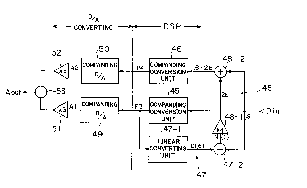
Fig. 6 shows the basic structure of the D/A
converting apparatus relating to the first embodiment
of this invention. In Fig. 6, after the above
respective processes are performed in the DSP ~later
recited in Fig. 12) digital signal Din, input as a
linear PCM code, is applied to first companding
l~l100~
- 27
conversion unit 45 and is converted to the first
companding PCM code P3. The first companding PCM
code P3 is input to the first D/A converting system.
This system comprises first companding D/A converter
49 for converting code P3 to the first analog signal
A1, and first amplifier 51 for amplifying the signal
A1 k3 times.
At least second companding converting unit 46,
detecting unit 47 and noise adding unit 48 are formed
10 in the DSP in addition to converting unit 45.
Detecting unit 47 detects a quantizing noise N in the
first companding PCM code P3. Detecting unit 47
comprises linear converting unit 47-1 and subtracting
unit 47-2 in Fig. 6.
Quantizing noise N is applied to noise adding
unit 48. It is then multiplied by k4 and added to
digital signal Din. In Fig. 6, noise adding unit 48
comprises amplifying unit (gain k4) 48-1 and adding
unit 48-2. The output of noise adding unit 48 is
20 converted to the second companding PCM code P4 by
second companding converting unit 46. The code P4 is
input to the second D/A converting system. This
system comprises the second companding D/A converter
50 which converts code P4 to the second analog signal
134006~
- 28
A2, and second amplifier 52 which amplifies the
signal A2 k5 times. The relations between k3, k4 and
k5 are determined to satisfy the conditions k3 + k5 =
1, and k4 = k3/(1 - k3), where k3, k4 and k5 are all
positive real numbers.
Respective amplification outputs of the first and
second analog signals, A1 and A2, obtained by the
above process are added at adder 53, thereby producing
analog conversion output AoUt.
An operation of the first embodiment shown in
Figs. 5 and 6 will be explained.
Firstly, the A/D converting apparatus of Fig. 5
is explained. Supposing that the amplification ratio
k1 of the first amplifier 38 satisfies k1 = k
(therefore, the amplification ratio k2 of the second
amplifier 40 satisfies k2 = 1/k) and that the
amplitude of analog signal Ain is a. The signal Ain
is amplified to provide ak and ~/k, which are applied
as input to corresponding companding A/D converters 39
and 41, thereby providing the first and second PCM
codes P1 and P2 of digital values. These PCM codes
are subjected to companding and are not real numerical
values. Therefore, the PCM codes cannot be a subject
of a computation and they are modified. Therefore
1 3 4 i) O G ~
- 29
these codes are returned to linear codes L1 and L2
representing the real numerical value by linear
converting units 42 and 43. In this state, arithmetic
operation unit 43 performs an arithmetic operation to
obtain an average value (L1 + L2)/2. As described in
detail later, in addition to a group of 255 or 256
output values which may be output as 8 bit companding
CODEC, an intermediate value within two adjacent
output values may be produced from the average value,
thereby resulting in an increase in the kinds of
output values. This means an increase in the
resolution of the A/D converter. The reason is that
the linear codes L1 and L2 differ from each other
because of the multiplication ratio of k and 1/k and,
if L1 is the same value L as L2, then the value L is
the output value and, if L1 deviates from L2, the
intermediate value between L1 and L2 appears as the
output value.
The above operation will be explained in more
detail by referring to an example.
In the A/D converter of Fig. 5, the
amplification ratio k1 of the first amplifier 38 is
set at K (=1.01), and the amplification ratio k2 of
the second amplifier 40 is set at 1tk~=1/1.01). An
1340~6~
- 30
explanation of this embodiment adopts a ~-law as an
example of a companding rule. Even in case of an A-
law, the effect of the present invention does not
differ.
Fig. 7 shows a relation between respective values
under a general ~-law. In Fig. 7, the range of the
analog voltage input (a column of linear input in the
drawing) added to companding A/D converters 39 and 41
of Fig. 5 is set, for example, -8158 to +8158 and 28
(=256) times the output value (OUTPUT VALUE) are set
within the input analog voltage range. The unit of
the analog input voltage is, for example, milli-volts.
In accordance with the respective value of the analog
inputs (linear inputs in the drawing), an 8-bit
digital code is determined as a ~-law PCM output,
and it outputs from the A/D converter. In Fig. 7, to
simply recite an explanation, only positive linear
input is shown, only the complete fourth segment is
recited and intermediate values in the other segments
are omitted. The segment means a range of respective
bent lines when a ~-law characteristic is expressed by
a plurality of bent lines.
An 8-bit digital code of the above ~-law PCM
output is simply a symbol used for a classification
. .
0 ~ 1
- 31
and does not mean an actual amplitude value.
Therefore, the above l~-law PCM output is converted to
the corresponding digital value of 0 to 8031 (which
corresponds to the output value (OUTPUT VALUE) in Fig.
7~ by first and second linear converting units (ll/L
converting units) 42 and 43 in the DSP of Fig. 5.
Thus, the digital value has 14-bit accuracy.
As the first and second linear codes L1 and L2 of
Fig. 5, numerical data corresponding to ~k and (x/k
10 appear, as explained above. For an 8-bit companding
A/D converter, the kind of respective output level of
the linear codes L1 and L2 are respectively merely of
255 or 256 types. However, the actual analog inputs
are a continuous value within the range of -8158 to
+8158, and the number of kinds of analog inputs is
16316 even when the integer portion only is
considered. Because of the difference between the
kinds of output levels of first and second linear
codes L1 and L2 and the continuous value of analog
20 input, a quantizing noise as described above occurs.
Generally speaking as an evaluation item of an A/D
converter and a D/A converter the above recited S/N
(in units of dB) is used. For example, for an 8-bit
companding A/D (D/A) converter for a telephone signal,
1340064
- 32
the output obtained by inputting a sine wave signal of
101OHz to the A/D converter is input to the D/A
converter. The D/A converter provides output
including a signal component, namely, a signal of
101OHz. This signal component, represented by an
"S" frequency component other than the 1010 Hz
included in the output from the D/A converter, is
represented by N (noise). A large part of the noise
comprises quantizing noise caused by representing a
certain range of analog input by an output value
formed by the central value of the analog input.
Therefore, a large S/N means a small quantizing
noise and a small waveform distortion. In other
words, to increase S/N it is necessary to decrease
quantizing noise, and to decrease quantizing noise
it is necessary to increase the output value from the
A/D (D/A) converter and to thereby decrease the
length of the quantizing steps.
According to the embodiment shown in Fig. 5, use
of two sets of 8-bit companding A/D converters 39 and
41 enables the above output value to increase as shown
below. Further, use of a commercially available
PCM.CODEC enables a signal processing apparatus to be
realized at a lower cost than with one set of higher
13~00~4
quantizing precision (or more than 8-bit) A/D
converters, even if two sets of 8-bit companding A/D
converters 39 and 41, are utilized.
In Fig. 5, the output value of the first and
second linear codes L1 and L2 are respectively D(a k)
and D (a/k). If k is not determined as k=1.01, but as
k =1 , the linear codes L1 and L2 naturally have the
same output value. As is shown in the preferred
embodiment, if k=1.01, the first amplification ratio
1.01 is slightly different from the second
amplification ratio 1/1.01. Thus, a k becomes
different from a/k. If the difference between ~ k and
a/k is small anda k and a/k is within a range of
respective rows shown in a column of a linear input
shown in Fig. 7, the output value D (~ k) is
coincident with that of D (a/k). In contrast, if the
difference between ak and a/k is outside the range
of repsective rows, the output D (a k) is different
from that of D(a/k). Namely, where k~1 but is a value
near 1, or where one of them is entered into the
adjacent range, the output value corresponding to the
adjacent range is produced and D(a k)~D(a/k). In the
former ( coincidence) an average value of ak and a/k,
namely, 1/2 x a{(k+1/k)} is positioned near the center
l~4oo6~
- 34
of the range of respective rows of the linear input
shown in Fig. 7. In the latter ( non-coincidence) the
above average value appears near the boundary between
adjacent ranges of respective rows.
In the arithmetic operation unit 44 in Fig. 5,
the average value of the first and second linear codes
Ll and L2 is set at DoUt =1 /2 ~(D(a-k)+D( ~/k)}
through an arithmetic operation, and in the latter
case explained above, the output DoUt becomes an
intermediate value between the output value of one row
and that of its adjacent row. In the former case,
namely, when a k anda/k are within the same range, L1
and L2 become the same, thereby enabling the average
value of L1 and L2, or the output DoUt to become the
same value as the respective output value. The output
value shown in the column of the output value (OUTPUT
VALUE) in Fig. 7 and a new output value mid-way
between adjacent output values are obtained, thereby
achieving the same result as a high resolution A/D
converter.
Fig. 8 shows the relationship among respective
values in an A/D converter and shows concrete
numerical values of an amplitude a of analog signal
Ain, output value ~k of the first amplifier 38,
1~00~'1
output value a/k of the second amplifier 40, D( a k)
(the value of the first linear code L1) , D( a tk) (the
value of the second linear code L2 ), and 1 /2 {D( a k) +
D( a/k)} (digital conversion output DoUt) with regard
to the apparatus shown in Fig. 5. It should be noted
in Fig. 8 that, as shown on the right side, the output
values shown by Q1, Q2 , Q3 and Q4 appear as new output
values in addition to ordinary quantizing output
values Q2', Q3' and Q4' of companding A/D converters
10 39 and 41. Their relationship is shown more
comprehensively in Fig. 9. Respective ones of Q2 ',
Q3 ' and Q4 ', for example, in Fig. 9 correspond to
those in Fig. 7. With regard to D(a k) and D(a/k)~ if
a is positioned within a region A, quantizing output
of the above two values is commonly Q3'. Thus, the
digital conversion output DoUt is also Q3', and if ~
is positioned in a region B, the respectlve quantizing
outputs are divided into two parts Q4 ' and Q3 ' . Thus,
the digital conversion output DoUt becomes an
intermediate value, Q3. In a case where a is
positioned in the region C, respective quantizing
outputs are divided into Q3' and Q2'. Thus, the
digital conversion output DoUt becomes an intermediate
value Q2.
- . .. .,. .. ... , . ~ , . ~ .. . " . , ,
1340064
- 36
As described above, conventionally, there are 255
kinds of output values, and in this embodiment the
number of kinds of the output values doubles and the
size of the quantizing steps (A) halves. Then,
quantizing noise power (~2/12) becomes 1/4 and S/N
increases by 6dB. When DSP processing is applied to
the digital conversion output DoUt, deterioration of
S/N is suppressed to a minimum value.
In this case, as shown in Fig. 9, suppose that an
upper value is obtained by subtracting 1/4 of a
quantizing step value q from the value of the upper
boundary (shown by a solid line) between two adjacent
quantizing output values q of companding A/D
converters 39 and 41 (Fig. 5), and that a lower value
is obtained by adding 1/4 of a quantizing step value
q to the value of the lower boundary. These values
then constitute new boundary values (i.e. decision
values shown by the dotted line), and the width of a
possible range of respective newly formed output
values become the same, which is the most preferable.
Thereby, an amplification ratio k can be calculated as
follows.
k'-~1 + (quantizing step)/(4 x ¦output value¦).
For a companding A/D conversion, the quantizing
l34~a~
step is made large in a region where the output value
is large (namely, the quantizing noise is large).
Thus, the ratio of (quantizing step / ~ouput value¦ )
of the companding A/D conversion is generally closer
to the constant value than that obtained by the
linear A/D converter. If this ratio is constant, then
the value of the above k can be determined.
However, as is clear from Fig. 7, the ratio of
(quantizing step / loutput value¦) is not always
constant. A part of the 8th segment has a value of
256/8031(=3.18%) and a part of the second segment has
a value of 4/33(=12%), and the difference between
these values is large. Therefore, it is necessary
to determine the most appropriate value
experimentally. Therefore, according to the result of
the experiment using ~-law 8 bit companding A/D
converter, k=1.025 is the most appropriate value.
Next, an operation of the D/A converter in Fig. 6
will be explained. In order to simplify the
explanation, it is supposed that the amplification
ratio of the first amplifier 51, is k3=2/3. Therefore
as described above, k4=k3/(1-k3)=(2/3)/(1-2/3)=2,
k5=1-k3=1/3. Under this condition, if the value of
digital signal Din of Fig. 6 is ~, Din is input to the
1340064
- 38 -
first companding D/A converter 49 through the first
companding converter 45 and is then converted to the
first analog signal Al . Thereafter it is multiplied
by 2/3 I=k3) by the first amplifier 51, the output of
which is 2/3D (~ ). Then the first companding PCM code
P3 is input to linear converting unit 47-1 and
reconverted to a linear signal. Therefore, the output
value (OUTPUT VALUE) D ( ~) corresponding to the
digital signal Din (=~) on the input side can be
recognized as a digital value. The difference between
the valu~ ~ of the digital signal Din and output value
D(~) is arithmetically operated in subtracting unit
47-2. Then a voltage E corresponding to a quantizing
noise N produced from companding conversion unit 45
through D/A converter 49 can be obtained. Namely,
E = ,3 - D ( ~ ) . . . (1 )
The above E is multiplied by 2(=k4) by amplifying
unit 48-1 and is then added to input signal Din.
Thereafter it is input to the second companding
conversion unit 46. Namely, B + 2E is input to
conversion unit 46 and is rewritten using the above
equation (1) as follows.
+ 2E = D(,~) + 3E . . . (2)
Where I E I is smaller than 1/2 a quantizing step
l3~0as.l
- 39
~expressed as q) corresponding to or closest to output
value D( ~) because, if the voltage E of the quantizing
noise N is larger than 1/2 a quantizing step, D(~)
becomes an adjacent different output value. As shown
in Fig. 7, if D(~ ) is an output value 359, ~ of a
linear input is 351 to 366, and thus, the quantizing
error is less than +8. This is less than 1/2 a
quantizing step 16 of a segment 4. Therefore 3 ¦E~ in
equation ~2) is less than 3/2 times the nearest
quantizing step q of D(~).
Value D(~ + 2E) of the second analog signal A2
obtained through a process of the second D/A converter
system of Din ~the second companding conversion unit
46~D/A converter 50 is classified in accordance with
the following conditions ~ ~ ~
Q where +1.5q > 3E ' 0.5 q:
D ( ~ + 2E) = D (~) + q ... (3)
where +0.5q > 3E > -0.5q:
D ( ~ + 2E) = D (~) ... (4)
~ where -0.5q > 3E - -1.5q:
D ( ~ + 2E) = D (~) -q ... (5)
D(~) +q is an output value adjacent to the upper side
of the output value D (~), and D (~) -q is the output
value adjacent to the lower side of the output value D
~ .. . . . . ~
1340064
- 40
~). The output value is multiplied by 1/3 (=k5) by
the second amplifier 52 in Fig. 6, and is then added
to the aforementioned output 2/3 D (~) of the first
D/A converter system in adder 53. Based on this
output 2/3 D (~) and the result of the above equations
(3) - (5), the added output AoUt is classified in
accordance with the following conditions
where +1.5q > 3E _ 0.5q:
2/3D(~) + 1/3{D(~) + q}=D(~) + q/3 ...(6)
~ where +O.Sq > 3E > -0.5q:
2/3D(~) + 1/3D(~) =D(~) ... (7)
where -0.5q > 3E ' -1.5q:
2/3D(~) + 1/3{D(~) - q}=D(~) - q/3 ...(8)
The relationships shown in the equations (6) -
(8) are shown in Fig. 10. For a conventional
structure in which only one set comprising a
companding conversion unit and a companding D/A
converter is provided, all the values of input digital
signal Din within a range designated by region A of
Fig. 10 is represented by an analog signal D (~).
Therefore, if digital signal Din is positioned within
region B, quantizing error is small, but if it is in
region C or D, it becomes large. In contrast, in the
above embodiment, quantizing error can be decreased as
13~0~
- 41
described below.
Condition ~ in the above equations ~3) or (6) is
rewritten as 0.5q > E ~ 0.5q/3. Namely, this shows a
range of voltage E of a quantizing noise of value ~ of
digital signal Din and representative value D(~) under
condition ~. This shows that the value ~ of digital
signal Din in Fig. 6 is within region C in Fig. 10.
Namely, deviation of ~ from the value D(~) represents
the value within the range is about 1/3 that of
quantizing step q. In such a case, as shown in the
aforementioned equations (3) and (6) the value of
analog signal AoUt is obtained by adding q/3 to the
representative value D(~). In other words, if the
value ~ of digital signal Din in Fig. 6 falls within a
range C of Fig. 10, the output of first companding D/A
converter 49 in Fig. 6 is D(~) and the output of
second companding D/A converter 50 is D(~) + q as
expressed in the above-recited equation (3).
Therefore, the respective outputs of first and second
amplifiers 51 and 52 are 2/3D(~) and 1/3~D(~) + q~ and
these outputs are added in adder 53, thereby producing
analog signal Aout of {D(~) + q/3} as is clear from
the equation (6) of Fig. 10. Conventionally, if the
value ~ of digital input signal Din is within a range
13 11~064
- 42
A in Fig. 10, analog signal AoUt is expressed merely
by D(~). In the present embodiment, if ~ is
positioned within a range C which is included in a
range A, Aout can be expressed by {D(~) ~ q/3},
thereby reducing quantizing error included in ~ and
AoUt. As a result, the quantizing error between the
analog signal AoUt and the value ~ in the range C
becomes small.
In condition ~, shown by the aforementioned
equations (5) or (8), the relationship is completely
opposite to that of the above condition ~ . The
analog signal AoUt obtained by subtracting q/3 from
the representative value D (~), and the quantizing
error between analog signal AoUt and the value ~ of
the region D becomes small.
For condition ~, shown by the aforementioned
equations (4) or (7), the value ~ is close to the
representative value D (~). This value is produced
as analog signal AoUt without modification.
As described above and shown in Fig. 6, the
above quantizing noise produced from the first D/A
converting system comprising a route of Din ~first
companding converting unit 45 ~first companding D/A
converting unit 49, is superimposed on an input signal
13400fi4
- 43
of the second D/A converting system comprising the
route of Din + second companding converting unit 46
~ second companding D/A converting unit 50.
Therefore, the quantizing noise from the first D/A
converting system is almost cancelled and the second
D/A converting system produces a maximum quantizing
noise of q/2. At the output of adder 53, the output
from the second D/A converting system is multiplied by
1/3 (=k5) by second amplifier 52. Thus, the produced
quantizing noise becomes q/6 at maximum, namely, 1/3
the conventional quantizing noise.
In the embodiment shown in Fig. 6, the output
value becomes 3 times that obtained with only an
ordinary companding D/A converter, and this
embodiment can provide a companding D/A converter of
an equivalent high resolution corresponding to, for
example, 9.5 bits ~256 x 3 -.29 5).
The above operation will be explained in more
detail by referring to an example. In an explanation
of this embodiment, a ~ -law is adopted as a
companding rule as in Fig. 5, and the effect of the
present invention does not differ from this embodiment
even if an A-law companding rule is adopted.
Figs. 11A and 11B show the value of respective
13~00fi4
_ 44
portions of the D/A converting apparatus shown in Fig.
6 and correspond to Fig. 7 regarding the A/D
converting apparatus. Figs. 11 A and 11B show
amplitude ~ digital signal Din, first companding PCM
code P3, value D ( ~) of analog signal A1 (digital
expression), quantizing noise N (digital value), the
value of two times voltage E of quantizing noise N
(digital value), a digital output from adder 48-2 (~
+2E), second companding PCM code P4, second analog
signal A2 and analog converting output AoUt {=(2/3 x
A1) + (1/3 x A2)}, respectively, in Fig. 6. As shown
in Figs. 11 A and 11B, respective analog converting
outputs AoUt appear at equal intervals of 5.333
between respective analog converting outputs.
Companding D/A converters 49 and 50 in Fig. 6
completely correspond to companding A/D converters 39
and 41, and respective quantizing outputs appear at
equal intervals of 16 between respective outputs for
segment 4, for example, as shown in the output value
20 (OUTPUT VALUE) in Fig. 7. Therefore, according to
Figs. 11 A and 11B, the output intervals of analog
converting output AoUt can be divided into small steps
which are 1/ 3 those of an ordinary D/A converter, and
the number of output values thus becomes 3 times that
..
1340064
- 45
of an ordinary D/A converter, by combining D/A
converters 49 and 50.
In the above embodiment, the case of k3=2/3 is
shown. However, for k3=1/2, calculations similar to
those of aforementioned equations (3) - (8) are
conducted, and the number of output values from
analog converting output AoUt are double and are
equal to those of a 9-bit companding D/A converter,
although an 8-bit companding D/A converter is adopted.
For k3=3/4, the number of output values becomes
4 times, and is equivalent to a 10-bit companding D/A
converter, although an 8-bit companding D/A converter
is adopted.
Fig. 12 shows a detailed circuit diagram of the
preferred structure of the A/D and D/A converting
apparatuses according to the present invention. The
preferred structure means that it can be constructed
by using two sets comprising a commercially available
DSP, a commercially available PCM.CODEC, and a few
other elements. According to this structure, a
practical, high-resolution A/D and D/A converter
apparatus can be realized by merely adding an
inexpensive and commercially available PCM.CODEC.
This can be done more efficiently than when a high
13 lOOfi4
-- 46
resolution A/D and D/A converting apparatus is
constructed using the aforementioned Fig. 2
structure.A hybridtransformer, amplifier and coarse
attenuator are omitted as shown in Fig. 12.
In Fig. 12, two companding A/D converters 39 and
41, as in Fig. S, and two companding D/A converters 49
and 50, as in Fig. 6, are provided by two companding
A/D converters and two companding D/A converters being
installed in first PCM.CODEC 54 and second PCM.CODEC
55 in which a pair of A/D and D/A converters is
integrated. In Fig. 12, arithmetic operation
amplifier 56 provides an amplification ratio k1 (Fig.
5) by using registers R~ and R2 (k1=R2/R1) and
registers R3 and R4 in the next stage form an
amplifier ratio k2 (Fig. 5). If k1 and k2 are k and
1 /k, respectively, as described above, k-R3/(R3 ~ R4)
= 1 /k, thereby determining the values of R3 and R4.
A similar analysis will be applied to an
operational amplifier 57 of a D/A converting system
and an amplification ratio k3 (Fig. 6) is determined
as R7/R6, and k5 is determined as R7/R5. Thus, analog
conversion output AoUt is obtained from {(R7/R6) x A1 }
+ {(R7/R5) x A2 } (A1 and A2 are recited in Fig. 6).
In the previous example, it is assumed that k3=2/3 and
1340064
-- 47
k5=1/3, and in this example, it is determined that R6
=1.5R7 and Rs=3R7-
The DSP comprises the above recited first andsecond linear converting units 42 and 43, an
arithmetic operation unit 44 (which calculates the
average level) in Fig. 5, the first and second
companding converting units 45 and 46, linear
converting unit 47-1, subtracting unit 47-2,
amplifying unit 48-1 and adding unit 48-2 as shown in
Fig. 6. Line 60 in Fig. 12 is a leak cancelling line
for preventing signals from leaking into a line in a
2-wire - 4-wire converter (hybrid trans), not shown
in Fig. 12. DSP function units 58 and 59 respectively
comprise a function of an equalizer (EQL) and a
function of an attenuator (ATT), for example. These
lines, connected to DSP function units 58 and 59, are
respectively connected to linear/l~ converting unit
(L/l~) 61 and ~/linear converting unit (ll/L) 62, and
are thus connected to a transmission path.
As explained above, the first embodiment provides
A/D and D/A conversion apparatuses which combine an
A/D and a D/A converter with a DSP, and the high
resolution input and output of an A/D and D/A
converter which is required by a DSP can be achieved
I3~0064
-- 48
by merely adding inexpensive amplifiers (amplifiers
38 and 40 in Fig. 5 and amplifiers 51 and 52 in Fig.
6) by utilizing an arithmetic operation function of
the DSP without modifying the A/D and D/A converters.
The ~econd ~mbodiment
Next, the second embodiment of this invention
will be explained. The present embodiment is
characterized as a clock of a digital signal processed
within a DSP changed, for example, from the first
clock (receiving clock) to the second clock
(transmitting clock) with signals kept in digital
form.
Figs. 1 3A and 1 3B are basic block diagrams of the
second embodiment of the present invention. Fig. 1 3A
uses a high-sampling digital low pass filter and Fig.
1 3B uses a high-sampling digital low pass filter which
is divided into a plurality of blocks.
As shown in Fig. 1 3A, data strings of the first
clock pass data converting circuit 63, and the number
of data per unit time is n (n>1, and is an integer)
times the original data. The output of converting
circuit 63 is input to interpolation processing unit
~'~ 6
65 through high-sampling digital low pass filteri~
1 3 ~
- 49
which operates at a sampling rate n times that of the
first clock.
Interpolation processing unit 65 forms and
outputs conversion data synchronized with the second
block by using an interpolation method, based on
timing difference I between the first and second
clocks. The timing difference is detected by timing
difference detection circuit 66.
As shown in Fig. 13B, high-sampling digital low
pass filter 64 (Fig. 13A), which operates at a
sampling speed n times that of the first clock, is
divided into a plurality of blocks 67, 68 and 69. The
ratio of the sampling speed between adjacent blocks is
made an integer, and the last stage block 69 operates
at a sampling speed n times that of the first clock,
and the sum of the loss characteristics of respective
blocks 67, 68 and 69 is made the same as that of the
original filter 64 of Fig. 13A.
Data conversion circuits 70 and 71 for outputting
the same amplitude data whose number is equal to the
ratio (Q2/Q3) of the sampling speed between adjacent
blocks with regard to one item of input data are
provided between respective blocks of a high-sampling
filter. Data conversion circuit 63' to which the
134006l
- 50
first clock data trains are input, is set to produce
the same amplitude data whose number is equal to the
ratio Q1 =n/Q2/Q3 of the sampling speed of the first
stage block 67 to that of the first clock per unit
time, as compared with the number of original data.
This will be explained later.
In Fig. 13B, where the sampling rate of the first
stage block 67 is the same as the rate of the first
clock, namely, fa (Q1=1), then data conversion circuit
63' is not necessary.
The general operation of the above basic
structure will be explained. Figs. 14A to 14C are time
charts of a waveform of various portions of Fig. 13A.
Hereinafter, the frequencies of the first clock
and the second clock will be designated as 8KHz.
In Fig. 13A, data conversion circuit 63 receives
data values Sn, Sn+1, Sn+2, Sn+3,... of a sine wave
of, 3.004KHz ,for example, at time of the first clock
tn~ tn+1~ tn+2~ tn+3~ ~-- as shown in Fig. 14A. The
number of data per unit time is n times, for example,
8 times, that of the original data as shown in Fig.
14B. Then, the output of data conversion circuit 63 is
applied to high-sampling digital low pass filter 64
which operates at a sampling speed of 64KHz, which is
1340û64
- 51
8 times faster than the first clock. A cut frequency
of the filter 64 is the same as that allowed for the
data system train of the first clock and is (8/2)KHz =
4KHz for voice signals. Therefore, the above filter
64 produces such a signal as shown in Fig. 14C.
The time interval of these signal trains becomes
1/8 those of the signal synchronized with the first
clock.
Even if we try to obtain the data values at the
time of the second clock Tn 1I Tnl Tn+1, Tn+2, Tn+3l
... by using respective data values Snl Sn+1, Sn+2,
Sn+3l ... at the times of the first clock tn~ tn+1,
tn+2, tn+3l ... by Lagrange's interpolation method,
the time intervals between respective data are wide
and the variations of the data values are large.
Thus, the data values at the time of the second clock
Tn_1, Tn... are difficult to obtain. If the time
interval of the first clock is made 1/8 that of the
signal synchronized with the first clock, as shown in
this embodiment, the time interval between respective
data becomes narrow. This decreases the variation in
data values within a time interval between two
timings, for example, between adjacent timings, and
enables the data values at the time of the second
1 3~0064
- 52
clock~ Tn-1~ Tn~ Tn+1~ Tn+2~ Tn+3r ... to be obtained.
As shown in Fig. 14C, the timing difference T
between the first and second clocks is obtained by
timing difference detection circuit 66, and is input
to interpolation processing unit 65. Interpolation
processing unit 65 can obtain the data value F at a
time of the second clock Tn+1 by using a period ~a
of the first clock, the difference ~ between the
time of the second clock Tn+1 and the 1/8 time
interval which exceeds the time Tn+1, and the data
values Fm 1 and Fm of the 1/8 time intervals at both
sides of the time of the second clock Tn+1, and also
using the following Lagrange's interpolation formula,
F= ~F {( Ta/n - ~} + Fm_1 ~ a
As described above, the data values F at times of
the second clock Tn_1~ Tn~ Tn+1' Tn+2~ Tn+3~ ~-- a e
produced as digital data values at the second clock.
According to the above approach, a digital signal
is not converted to an analog signal. Thus, a
quantizing noise is not produced and the apparatus is
subject to all digital processings, thereby being
miniaturized as an integral circuit.
A high sampling digital low pass filter 64 of
1340064
- 53
Fig. 13A operates at a repetition frequency of 8 times
the sampling frequency of the original data .
Namely, as 8 data are input and 8 data are output
during a repetition period of a sampling frequency of
the original data, the amount of processing becomes 8
times that achieved when it operates at the sampling
frequency of the original data.
If the order or degree of the high-sampling
digital low pass filter 64 is 6 and the order of the
delay equalizer for suppressing the group delay
distortion occurring in the filter is 2, thereby
totally providing the 8 order filter, the
equivalent order number in respect of a processing
amount is 64.
A digital filter performs one calculation of a
following difference equation with regard to every
second order.
yn=a xn + b xn_1 + C~xn-2 ~ d Yn-1 ~ e'Yn-2
Thus, the number of a multiplication is 5 per period
and 160 per period in the 64th order. Therefore,
other programs are performed by the DSP in processes
of more than 220 steps including a data conversion
processing.
Even if a high speed digital signal processing
.
1340064
- 54
unit in which the processing time per step is 100ns,
only 1250 steps at maximum can be used when the period
is 125 11 s (8KHz), and if 220 steps selected from
among these 1250 steps are assigned to a filter
calculation in the clock changing method, a
distribution of time to other processings decreases.
Thus, it is not preferred.
Therefore, as shown in Fig. 13B, the filter is
divided into a plurality of blocks and a process which
can be performed at a relatively low sampling speed is
processed by a filter of a low sampling speed, and the
amount of processing may be greatly reduced.
A process in a delay equalizer is related to a
pass band, and a frequency delay of more than the
cutoff frequency, for example 4KHz, need not be
considered. It can be conducted by filter block 6 7
which operates at the sampling speed of the original
data 8KHz.
Next, the cutoff frequency component from 4KHz
to 8KHz is performed by filter block 68 which operates
at a sampling speed of 1 6KHz. A cutoff of a frequency
component from 8 KHz to 32KHz is performed by filter
block 69 in the last stage which operates at the same
sampling speed, 64KHz, as that of the high-sampling
)Ofi4
-- 55
digital low pass filter 64 of Fig. 13A.
In this example, the sampling speed of the first
stage block 67 is the same as that of the first clock,
and data conversion circuit 63' is not necessary.
Data conversion circuit 70 is for outputting two
data of the same amplitude regarding input data on the
input side of filter block 68. Data conversion
circuit 71 is for outputting four data of the same
amplitude regarding one item of input data on the
10 input side of filter block 69.
As constructed in the manner described above,
respective blocks 67 and 69, having sampling
frequencies of 8KHz and 64KHz, are formed of a filter
of the second order, and block 68, having a sampling
frequency of 16KHz, is constructed of a filter of the
fourth order. Then, the total number of
multiplications per period becomes 5 x 1 + 5 x 2 x 2 +
5 x 2 x 4 =65. From the relationship of the order
ratio with the sampling ratio, the number of
20 multiplications for each second order is 5. This
greatly reduces the amount of calculation.
In the apparatus constructed as shown in Fig.
13B, described above, the number of output data from
filter block 69 is 8 times the original data and is
~34006~
- 56
the same as that of the filter of Fig. 13A. The
interpolation processing unit 65 can perform a change
from the first clock to the second clock in the
manner shown in Fig. 13A.
The structure and operation of respective parts
of Figs. 13A and 13B will now be explained in detail.
Fig. 15 shows a block diagram of data conversion
circuit 63 of Fig. 13A, Fig. 16 shows a block diagram
of high-sampling digital low pass filter 64, Fig. 17
shows the amount of attenuation of the filter in Fig.
16, Fig. 18 shows a flow chart of a program of
interpolation processing unit 65 shown in Fig. 13A,
and Fig. 19 shows a principle block diagram of timing
difference detection circuit 66.
In the respective figures, 72 is a memory, 73 and
109 multipliers, 108 a 10-bit counter, 110 a 10-bit
register, 111 a switch, 74 to 77 adders, 78 to 87
data delay memories, and 88 to 107 coefficient
multipliers.
The data conversion circuit in Fig. 15 produces
the same data 8 times per period. It receives, for
example, 16-bit amplitude data at intervals of, for
example, 8KHz, and writes them in memory 72 in
synchronization with the first clock, and produces the
134006~
data 8 times per period by using a read clock obtained
by modifying the first clock 8 times, using
multiplier 73.
Fig. 16 shows an example of a high-sampling
digital low-pass filter having a cut-off frequency of
3.8 KHz and comprising four sections, each containing
a two-order digital filter. Six orders of the above
filter construction cut off the frequency in the 4 to
60KHz band. The other 2 orders form a delay
equalizer for equalizing group delay time distortion.
The whole filter operates at a sampling speed of 64KHz
and performs 8 filter calculations per period of
8KHz.
The attenuation characteristic is shown in Fig.
17. The gain at around 3.4KHz is 2 - 3dB because
the RZ/NRZ correction is performed at this point, as
an input signal is subjected to NRZ processing.
The filter may be a large scale transversal
filter.
An interpolation processing is shown in the
operation flow chart of Fig. 18. When, for example,
the same data is input 8 times for Ta (as shown in
Fig. 14C) at a period of first clock, m of la m/8
(m=1 to 8) is sequentially increased from 1 at step S1
.
1340064
- 58
by comparing time difference T between the first clock
and the second clock. When the sign ofaT = Ta m/8 -
becomes positive, the comparison processing isstopped, and the difference a~ between time Tn+1 of
the second clock and the time of 1/8 time interval
which exceeds Tn+1, and the value of m are obtained.
In Fig. 14C, it is understood that m=5.
At step S2, the data value F of time Tn+1 of the
second clock is obtained from data values Fm 1 and Fm
when m=4 and m=5, based on the following Lagrange
interpolation formula,
F = ~Fm { ( Ta/n) - ~T} +Fm_1 ~ aT~ ~- ( Ta/ll) -
As described above, the data value can be
obtained at the time of the second clock Tn 1~ Tn'
Tn+1~ Tn+2~ Tn+3l ~-- as shown in Fig. 14A.
Fig. 19 shows the basic structure of the time
difference detecting circuit. The embodiment will be
explained in detail by referring to the third and
fourth embodiments.
The time difference detecting circuit of Fig. 19
multiplies the first clock by 21~ using multiplier
109. To provide input data to 10-bit counter 108,
it is reset at a rise of the first clock. Thus, its
count value shows a position in time obtained by
." . . .. .. . . . . . .. . . ~.
l~4no~4
- 59
equally dividing the period of the first clock by
21~=1024. Thus if the count value is, for example,
512, the time is shown to be exactly in the middle of
the first clock.
Therefore, at a timing of the second clock,
switch111 is turned on to obtain the value of counter
108 into 10-bit register 110, and to thereby obtain
time difference I between the first clock and the
second clock, at a resolution obtained by dividing a
period by 1024.
Next, it is explained where the clock changing
method of the present invention is applied to the PCM
r~ ~0
channel apparatus shown in Fig. 1-~.
Fig. 20 shows a block diagram of a digital PCM
'~ channel apparatus based on the second embodiment.
Parts designated by the same reference numbers as
those in the prior art device shown in Fig. 3 and the
base structure of the second embodiment shown in Fig.
13A perform the same functions.
In Fig. 20, receiving clock RCLK reproduced by
receiving timing reproducing circuit 115 from received
PCM signal RIN, and transmitting clock SCLK produced
by transmitting clock generator 114 of its own
station, exist as a clock timing. Receiving clock
~3400fi4
- 60
RCLK is input to receiving register 116, D/A converter
24, A/D converter 23, DSP 118 and transmitting and
receiving timing difference detecting circuit 66, and
most of the functions operate based on receiving clock
RCLK. On the other hand, transmitting clock SCLK is
input to transmitting register 113 and transmitting
and receiving timing difference detecting circuit 66.
Therefore, in the circuit of Fig. 20, input
signal SIN from a subscriber is picked up by receiving
clock RCLK, and receiving PCM signal RIN from the
other station is written into receiving register 116.
The receiving PCM signal RIN is read out by receiving
clock RCLK and is converted from a PCM signal of a~-
law companding rule to 16-bit linear data, for
example, by ~/L converter 117, and is input to
receiving level setting-equalizer 28. Transmitting
level setting-equalizer 27 on the transmitting side
and receiving level setting-equalizer 28 on the
receiving side perform respective corresponding
processes. Precision balancing circuit 29 bridging
transmitting and receiving system performs a process
on receiving clock RCLK, thereby preventing the
aforementioned problem from being produced by a clock
shift.
1340064
- 61
Output signal SOUT should be output on
transmission of clock SCLK. Thus, the above recited
clock changing process is conducted by the above
recited data conversion circuit 63, high sampling
digital low pass filter 64, interpolation processing
unit 65 and (transmitting and receiving) timing
difference detecting circuit 66 with regard to an
output data system of transmitting level setting-
equalizer 27. The signal is thus converted so that it
has an amplitude whose timing matches that of
transmitting clock SCLK. It is then converted from a
linear signal to a PCM signal according to a ~-law
companding rule by L/~ converter 112, and written
into a transmitting register. Data are read out from
this register on transmission of clock SCLK, and
transmitted in a jitter-free state to a multiplication
unit, not shown, as output signal SOUT.
In the above construction, data conversion
circuit 63, high sampling digital low pass filter 64,
and interpolation processing unit 65 are digital, and
can thus be integrated and miniaturized as digital
signal processor (DSP) 118 together with other digital
circuits. As (transmitting and receiving ) timing
difference detecting circuit 66 is also digital, it
1340064
-- 62
can be integrated and miniaturized as interface LSI119
together with other digital circuits. Obviously other
methods may be used for dividing the circuit shown in
Fig. 20 for the purpose of an integration. In Fig.
20, A/D converter 23 and D/A converter 24 are
constructed normally and if they are constructed as
shown in the first embodiment of Fig. 1 2, they
provide a great effect.
Next, the structure of a circuit for dividing a
high-sampling digital low pass filter into several
sections to decrease the number of arithmetic
operations will be explained in detail.
Fig. 21 shows the structure of the high-sampling
digital blocks of Fig. 1 3B divided into several
sections. Fig. 22 shows the amount of attenuation
of respective sections shown in Fig. 21, where (~) -
(~) correspond to filter blocks (~ 3 in Fig. 21.
Fig. 23 shows the whole attenuation amount of a filter
of Fig. 21.
In Fig. 21, 120 to 123 designate adders, 124 to
135 data delay memories, and 136 to 154 coefficient
multipliers.
Filter block (~ in Fig. 21 is a delay equalizer
and is related only to a passing band, and delay
1340~fi~
- 63
characteristics at a frequency higher than 4KHz in the
cutting-off range are not questioned. Thus, it
operates at the sampling speed ~ 8KHz) of the original
data, and the data conversion circuit ( 63' in Fig.
13B) is not required in the initial-stage.
Filter block ~ cuts off frequency components
from 4KHz to 8KHz and operates at a sampling speed of
16KHz. In this case, the data conversion circuit (as
shown in Fig. 13B) for outputting two pieces of the
data of the same amplitude in response of one piece
of input data, is required on the input side.
Filter block ~ cuts off frequency components
from 8KHz to 1 6KHz and operates at a sampling speed of
32KHz. In this case, the data conversion circuit
(shown in Fig.13B) for outputting two pieces of data
of the same amplitude in response to one piece of
input data, is also required on the input side.
Filter block ~ cuts off frequency components
from 1 6KHz to 32KHz and operates at a sampling speed
of 64KHz. In this case also, the data conversion
circuit for outputting two pieces of data of the same
amplitude in response to one piece of input data is
required on the input side.
The number of data output from filter block
13~0~
- 64
is 8 times that of the original data for the filter
shown in Fig.16. Filter block ~ thereby performs a
change from first clock to second clock using the
interpolation processing unit ( 65 in Fig. 13B).
- In this case, the number of multiplications per
period in filter block ~ is 5 x 1, as the number of
coefficient multipliers is 5. The number of
multiplications per period in filter block ~ is 8 x
2 as the number of coefficient multipliers is 8 and
the sampling speed is 16KHz. The number of
multiplications per period in filter block ~ is 3 x
4, as the number of coefficient multipliers is 3 and
the sampling speed is 32KHz. The number of
multiplications per period in filter block ~ is 3 x
8, as the number of coefficient multipliers is 3 and
the sampling speed is 64KHz. Thus the total number of
multiplications per period is 57. It will be
understood that this is much less than 160 in case of
the filter shown in Fig. 16
As described above, in the second embodiment it
is possible to change the data system trains of the
first clock to the data system trains of the second
clock using the digital form of data kept, thereby
eliminating the quantizing noise which causes a
.... . . . ... .
1~40064
- 65
problem in the prior art example shown in Fig. 4. In
the present invention, communication quality is not
lowered and this embodiment can be greatly
miniaturized by integration.
This embodiment can be integrated and
miniaturized together with other digital circuits, and
is made inexpensive.
The Third Embodiment
The third embodiment will now be explained. This
embodiment describes in detail timing difference
detecting circuit 66, shown in Figs. 13A and 20 in the
second embodiment, and also describes the structure of
transmitting register 113 shown in Fig. 20.
The present embodiment is based on the basic
structure shown in Fig. 19. According to the
principle shown in Fig. 19 and described above, a
counter is made operative after 10-bit counter 108 is
reset by the first clock (called receiving clock RCLK
hereinafter). The content of the above counter is
latched in 10-bit register 110 at the rising edge of
the second clock (called transmitting clock SCLK
hereinafter), thereby detecting a timing difference 1.
According to the above principle, time when the
13~006~
- 66
above latch is conducted at a rising edge of
transmitting clock SCLK, for example, a timing
difference ~ is produced. When T iS input to
interpolation processing unit 65 (in Fig. 13A or Fig.
20) in signal processor 118, which operates according
to receiving clock RCLK, the time is not constant from
the viewpoint of signal processor 118. Namely, the
timing difference ~ is input to the beginning or end
of the interpolation process (shown in Fig. 18).
Therefore, a buffer circuit is required for a time
adjustment.
When the period of transmitting clock SCLK is
slightly shorter than that of receiving clock RCLK,
the timing difference has to be detected twice during
a period of RCLK. Conversely, when the period of
RCLK is slightly shorter than that of SCLK, the
rising edge of SCLK does not occur within the period
of RCLK.
When the period of transmitting clock SCLK is
slightly shifted from that of receiving clock RCLK
there exist three cases, in which the number of input
data per period is 0, 1, and 2. In addition, the
time of occurrence of the input data is not constant.
Therefore, a buffer circuit is required between
1340064
- 67
transmitting and receiving timing difference detecting
circuit 66 and signal processor 118. The present
embodiment discloses a detailed circuit for
transmitting and receiving timing difference detecting
circuit 66, including a buffer circuit.
Fig. 24 shows a detailed circuit structure for
transmitting and receiving timing difference detecting
circuit 66 within the data PCM channel apparatus in
the second embodiment shown in Fig. 20.
In Fig. 24 Q-bit counter 155, latch 156 and
multiplier 157 are respectively the same as 10-bit
counter 108 (Q=10), 10-bit latch 110 and multiplier
109 in Fig. 19. The first clock and the second clock
respectively correspond to receiving clock RCLK and
transmitting clock SCLK.
When viewed from the signal processor side (118
in Fig. 20) the time at which timing difference data
I is produced from latch 156 is not constant as
described above. Thus, a case can occur in which
data of the previous period has not yet been
processed, when the process of obtaining data of the
present period based on receiving clock RCLK is
occurring. Therefore, two buffer circuits 159 and 160
are provided in parallel as shown in Fig. 24.
134~1~6~
- 68
Switches SW1 - SW6 are provided on the input side, and
are switched depending on whether the cycle number of
receiving clock RCLK is odd or even. Therefore, when
data from latch 156 is written into one of buffer
circuits 159 and 160, the other is connected to the
signal processor, thereby enabling data to be read
out. Signals obtained by dividing the frequency of
receiving clock RCLK into 1/2 the frequency of the
receiving clock by frequency divider 158 is used as a
control signal for switching an even number/odd number
cycle.
As described above, when the transmitting period
clock SCLK is slightly shorter than that of receiving
clock RCLK, the timing difference must be detected
twice during one period of RCLK, and before
completing processing of the data of the previous
period, the following data may be input. Therefore,
respective buffer circuits 159 and 160 have a two-
stage structure comprising respective memories #1,
#2, 161 and 162, and the content of these memories is
selected by selector 164.
In the above two-stage structure, data
corresponding to the address pointer is required to
designate how many pieces of data are input per
134006~
- 69
period, and input data number memory 163 for storing
the data is provided in respective buffers. As
described above, where the period of receiving clock
RCLK is slightly shorter than that of transmitting
clock SCLK, the rising edge of SCLK is not positioned
within a period of RCLK, and during such period,
signal processor 118 in Fig. 20 cannot perform a
process in interpolation processing unit 65. To make
this judgment, the above input data number memory 163
is necessary. Memory 163 is reset by a control
circuit, not shown, at the immediately preceding
timing, every time the memory is connected to the
latch circuit.
Signal processing unit 118 in Fig. 20 performs
the following operation in correspondence with
transmitting and receiving timing difference detecting
circuit 66 ~Fig. 20) shown in detail in Fig. 24.
Firstly high-sampling low pass filter 64 operates
continuously. Next, interpolation processing unit 65
obtains a timing difference ~ from transmitting and
receiving timing difference detecting circuit 66 at
every period of respective receiving clocks RCLK,and
performs the following processes. Namely, when the
contents of input data number memory 163 in the
l3~oo6~
- 70
currently selected buffer circuit (159 or 160) in
Fig. 24 is observed to be 0, it is unnecessary to
output transmitting output signal SOUT and an
interpolation processing is not conducted. When the
number of input data is more than 1, they are input
sequentially from the corresponding memory 161 or 162
through an operation of selector 164. Then,
interpolation processings are conducted, the number
being the same as that of data, thereby producing
output signal SOUT.
Next, an operation of transmitting register 113
in Fig. 20, corresponding to the above timing
difference detecting processing and interpolation
processing will be explained.
Output signal SOUT is arithmetically operated and
produced by signal processing unit 118, which operates
in synchronization with receiving clock RCLK.
Therefore, signal processing unit 118 produces an
output almost in synchoronization with receiving clock
RCLK. As already described, output signal SOUT should
be transmitted outwardly in synchronization with
transmitting clock SCLK. Thus, a buffer circuit is
required for time adjustment of output signal SOUT.
This is a function of transmitting register 113 in
.. , ., , . ,~.... . . . .. . . . . . . . .. . .
- 71 - 1340064
Fig. 20. The condition required for a register is as
follows.
Data input time from signal processing unit 118
to transmitting register 113 is independent of the
output time of output signal SOUT from the register.
The periods of receiving clock RCLK and transmitting
clock SCLK are slightly different, and they are always
moving relative to each other. Thus, over a
relatively long period, they inevitably sometimes
coincide. In this case, while data is being
transmitted outward from transmitting register 113, a
write process is conducted in the register, thereby
damaging transmission data. Therefore, while output
signal SOUT is output externally from transmitting
register 113, data should be prevented from being
transmitted from signal processor unit 118 to the
register 113.
The number of output data from signal processor
unit 118 is 0, 1, or 2 per period. As to output
timing, when two data are output per period they are
continuously output without a large time difference.
However, when a zero-data period is interposed
between two two-data periods, the next data will be
produced after two periods have passed. Therefore it
1340064
is necessary to adjust the timing to output data at a
time interval that matches transmitting clock SCLK.
In order to satisfy the latter condition,
transmitting register 113 in Fig. 24 comprises a
plurality of registers which are not described in
detail. Further, a judging circuit for determining
which data are output of the data stored in said
plurality of registers, is also provided. This
judging circuit may make a judgment, using the number
of data received from signal processing unit 118, and
the register number from which data are output in the
previous period, as a parameter. Therefore a counter
is provided for counting the number of received data.
In order to satisfy the former condition, a
control circuit for preventing input data from
entering a counter when the counter is reset, or when
the result of counting is being transferred, is
provided in transmitting register 113.
A detailed circuit relating to transmitting
register 113 will be explained in the following fourth
embodiment.
The Fourth Embodiment
The fourth embodiment will now be explained.
13~0064
- 73
This embodiment describes in detail (transmitting and
receiving) timing difference detecting circuit 66 in
Figs. 13A and 20, and also recites interpolation
processing unit 65 and transmitting register 113 in
Fig. 20. In this embodiment, an operation relation
between the first clock (receiving clock RCLK) and the
second clock (transmitting clock SCLK) with regard to
transmitting and receiving timing difference detecting
circuit 66 is reversed to that of the third
embodiment, thereby making the circuit structure
simpler than in the third embodiment.
Fig. 25 shows a block diagram of transmitting and
receiving timing difference detecting circuit 66 and
Fig. 26 shows an operation flow of signal processor
118 in Fig. 20 in the second embodiment.
In Fig. 25, the system clock of the second clock
produced in the data PCM channel apparatus in Fig. 20
is frequency-divided by frequency divider 165 to
provide 1/2L times the frequency of the second system
clock, thereby producing the second clock of
transmitting clock SCLK. This portion corresponds to
transmitting clock generator 114 in Fig. 20. As is
opposite to the apparatuses in Figs. 19 and 24, the
reference clock, namely, receiving clock RCLK in
.. ...... .. . ... .. .. ,, _ .. .. . . . . . . .. . . .
13~0064
_ 74
signal processing unit 118 is used as a latch signal
for latch circuit 167 in Fig. 25, and the second
clock of the system clock synchronized with SCLK is
used as a counting operation clock for L-bit counter
166.
By enabling an operation of latch circuit 167 to
be synchronized with receiving clock RCLK, an input
time of timing difference data to signal processing
unit 118 is determined to have the same relationship
as signal processing unit 118, which operates in
synchronization with RCLK.
Another feature of this embodiment is that
interpolation processing unit 65 (Fig. 20), which
operates as shown in Fig. 26, determines the number of
interpolation data to be operated wihin a period based
on receiving clock RCLK as follows. As the period of
transmitting clock SCLK differs by a maximum of 10-4
from that of the receiving clock, a timing difference
between the transmitting clock and the receiving clock
varies with period, gradually increasing or gradually
decreasing. Where the number of data per period with
reference to RCLK is 0 or more-or-less 2, the value of
the timing difference between two adjacent periods
changes greatly. Interpolation processing unit 65
13~006~
uses these characteristics and can recognize the
number of interpolation data to be calculated within a
period from a variation between a timing difference of
the present period and a timing difference of the
previous period.
As constructed above, a buffer circuit becomes
unnecessary in timing difference detecting circuit,
thereby enabling the circuit scale to be greatly
reduced.
An operation of transmitting and receiving timing
difference detecting circuit 66 and an interpolation
process in interpolation processing unit 65 will be
explained in more detail with regard to the fourth
embodiment, shown in Figs. 25 and 26.
In Fig. 25, a system clock with a frequency 2L
times that of transmitting clock SCLK is input to L-
bit counter 166 for a count operation. For example,
if L=10 and the frequency of SCLK is 8KHz, the
frequency of the system clock becomes 8.192 MHz. In
this case counter 166 indicates a count value from 0
to 2L-1. This count value is returned to 0 in
accordance with a period of transmitting clock SCLK,
thereby being reset at every period of transmitting
clock SCLK.
13~0064
- 76
When the count value is latched at a rising edge
of receiving clock RCLK, the value of the clock is a
timing difference based on transmitting clock SCLK
when the period of transmitting clock SCLK is 2L.
- Counter 166 can latch the count value without
stopping. Thus, the counter is always reset by SCLK
as described above.
The latch data is transmitted to an input
register, not shown, in signal processing unit 118 in
Fig. 20, by adding an L-bit transmitting clock to
latch circuit 167 immediately after the latch
operation is completed. Therefore, the time from a
latch operation to a transmission is very small and is
conducted at a predetermined timing within a
respective period, based on receiving clock RCLK. The
above transmission operation is thereby conducted in
synchronization with receiving clock RCLK.
On the other hand, signal processing unit 118
operates based on receiving clock RCLK, as described
above. This means that the difference between the
time at which various processes are conducted in
signal processing unit 118 and the time at which
receiving clock RCLK rises, for example, is constant.
Therefore, the period from the time at which timing
1340064
- 77
difference data is transmitted from latch circuit 167
to signal processing unit 118 to the time at which
the timing difference data is actually used, becomes
constant. When the length of this period is less than
the corresponding period based on transmitting clock
SCLK, there is no unused data remaining in an input
register when data is transferred from latch circuit
167 to an input register in signal processing unit
118. Therefore, a buffer circuit is unnecessary.
The operation of the present invention shown in
Figs. 25 and 26 is explained with reference to the
timing chart shown in Figs. 27A and 27B.
In Figs. 27A and 27B, the abscissa represents
time. In ~ in Figs. 27A and 27B, to~ t1~ t2, ...are
rising edge points of receiving clock RCLK and in ~ in
Figs. 27A and 27B, To~ T1, T2, ... are rising points
of transmitting clock SCLK.
Plot ' ' synchoronized with timing to~ t1~ t2,
... of receiving clock RCLK among the plots shown in
in Fig. 27A is an original item of data synchronized
with receiving clock RCLK input to data conversion
circuit 63 in Fig. 20. The other plots '-' represent
an output of high sampling low pass filter 64 of Fig.
20 and correspond to the second embodiment of Fig.
1~0064
14C. In Fig. 14C, the data are highly-sampled 8 times
per period, but in Figs. 27A and 27B, it is highly-
sampled 4 times per period to enable a brief
explanation. Further in ~ in the figure, plots 'O'
represented by S0, S1, S2, ... synchronized with
timings To~ T1, T2, ... of transmitting clock SCLK are
signal values to be outputted as output signal SOUT
after they are subjected to an interpolation process
in interpolation processing unit 65 in Fig. 20 and are
changed to transmitting clock SCLK.
Fig. 27A shows the case where the period length
(S period) of transmitting clock SCLK is larger than
the period length (R period) of receiving clock RCLK.
As the difference in period length between SCLK and
RCLK is 10-4 at maximum, the timing difference between
'~ and ~ is exaggerated for easy understanding.
L-bit counter clock 1 66 in Fig. 25 is
synchronized with receiving clock SCLK, so the
designated value of the counter is 0 at respective
timings of tn(n=0, 1, 2, .. ). At to~ t1~ t2, .. the
count value is latched and almost simultaneously
transmitted to signal processing unit 118 (Fig. 20).
The count value at this time, namely the timing
difference between transmitting clock SCLK and
1340064
- 79
receiving clock RCLK with transmitting clock SCLK made
as a reference, is designated by two lines when a
latch is performed, as shown by the upward-pointing
arrow.
As shown in ~ in Fig. 27A, the timing difference
decreases with time until it reaches 0, becomes a
maximum at the beginning of the next period, and again
gradually decreases. In such a period shown in T1 ~
T2 or T6 - T7, the arrow shows that two count values
are transmitted per period with reference to the
period of transmitting clock SCLK. However, from the
viewpoint of signal processing unit 118 for receiving
a transmission signal (signal transmitting unit 118
being synchronized with receiving clock RCLK), only a
single interpolation process of Fig. 26 is conducted.
In this case the timing difference (count value) at to
or t6 is very small and the timing difference at t1
or t7 is almost equal to the length of one period.
Based on these characteristics it is determined
whether the interpolation processing is conducted or
not, as described later.
In ~ in Fig. 27A, a time when an output signal is
output from output register Ro in signal processing
unit 118 to register R1 in an external timing
.. , _ . . . . .. . , . ~.
131006 1
- 80
adjusting circuit (the same as transmitting register
113 in Fig. 20) is designated by a row mark. An
output timing adjusting circuit will be explained
later. In Fig. 27A an output signal SOUT at T5 of
transmitting clock SCLK is transmitted to signal
processing unit 118 after a timing difference between
T5 and t5 is detected at t5, and an interpolation
calculation is conducted to provide S5. This S5 is
output to an output timing adjusting circuit at t5 5
~an intermediate time between t5 and t6) after 0.5 of
a period. Similarly, SOUT at T6 of SCLK is obtained
as S6 by detecting a timing difference between T6 and
t6 at t6 to transfer the timing difference to signal
processing unit118, and a calculation of an
interpolation is conducted, thereby providing S6. S6
is output to an output timing adjusting circuit at
t6 5 after 0.5 of a period. On the other hand, the
timing difference between T7 and t8 is detected at t8
and SOUT at timing T7 of SCLK is subjected to an
interpolation calculation, thereby enabling S7 to be
obtained. S7 is then output to an output timing
adjusting circuit at t8 5 after 0.5 of a period.
As is clear from the above, transmitting clock
SCLK, corresponding to a timing difference equal to
1340064
- 81
almost one period length detected at t1 or t7, does
not exist. Therefore the output signal SOUT (Fig. 20)
need not be output. In Fig. 27A, while transmitting
clock SCLK changes from T1 to T1o receiving clock RCLK
changes from to to t11. Therefore, the above fact
means that the output number of output signal SOUT
per unit time is less than that of receiving PCM
signal RIN (Fig. 20), as S period > R period.
Therefore the trend of timing difference is
made to correspond to an output operation of output
signal SOUT from signal processing unit 118 to an
output timing adjusting circuit. Then it is clear
that "from the viewpoint of a timing difference
determined by a rise of transmitting clock SCLK to a
rise of receiving clock RCLK and a period based on
receiving clock RCLK, output signal SOUT should not be
output to an output timing adjusting circuit in a
period when the timing difference of the previous
period is almost 0 and the timing difference of the
present period is about the length of a period". This
corresponds to the fact that the interpolation
process is conducted only once per period at the same
timing. The above control is realized according to
the operation flow chart of Fig. 26.
1340064
- 82
Next, Fig. 27B shows the case where the length of
the period (R) of receiving clock RCLK is larger than
the length of period (SCLK) of the transmitting
clock. In this case, also, for easy understanding,
- the timing difference between(~ and ~ is exaggerated.
Shown in ~ Fig. 27B, the timing difference
increases with time until it reaches a length equal
to a period, becomes 0 at the beginning of the next
period, and again gradually increases. This operation
is repeated.
Next output signal SOUT, at T5 of transmitting
clock SCLK, is transferred to signal processing unit
118 when the timing difference between T5 and t5 is
detected at t5 and provided as S5 through an
interpolation calculation. It is output to an output
timing adjusting circuit at t5 5 (intermediate
between t5 and t6) after 0.5 of a period. Next, SOUT,
at a timing of T6 of SCLK, is transferred to signal
processing unit 118 when the timing difference between
T6 and t6 is detected at t6, and then provided as S6
through an interpolation calculation. It is then
output to an output timing adjusting circuit at t6 5
after 0.5 of a period.
On the other hand respective output signals SOUT
13~0064
- 83
are considered at T7 and T8 of SCLK. In this case it
can be considered as similar to the case of T5 and T6.
When a timing difference between T7 and t7 is
detected at t7, SOUT at T7 is output to an output
timing adjusting circuit as S7 at t7 5 after 0.5 of a
period. However in Fig. 27B, the counter which starts
to count at T7 is returned to 0 at T8. Thus, the
timing difference between T7 and t7 is substantially
equal to that between T8 and t7, thereby transmitting
the value of the timing difference to signal
processing unit 118. Therefore, the output-to-output
value of the timing adjusting circuit at t7 5 becomes
an output signal S8 at the timing T8 of transmitting
clock SCLK. In this case an output S7 at a time
corresponding to T7 becomes insufficient.
To compensate for the insufficient output, the
present embodiment outputs signal S7 corresponding to
T7 to an output timing adjusting circuit before t7 5.
The timing difference value, in this case , is
equal to the timing difference between T7 and t7, and
can be considered as substantially a period length,
because the difference between receiving clock RCLK
and transmitting clock SCLK is only about 10-4.
Therefore, when the timing difference trend is made to
13400~4
- 84
correspond to the number of signals output from signal
processing unit 118 to an output timing adjusting
circuit, it is clear that "from the viewpoint of a
timing difference determined by a rise of transmitting
clock SCLK to a rise of receiving clock RCLK and a
period relating to a receiving clock RCLK, in a period
in which the timing difference of the previous period
is almost equal to a period and the timing difference
of the present period is almost 0, the transmitting
signal should be outputted to an output timing
adjusting circuit twice and the first output is
calculated by making the time difference equal to a
period and the second output is calculated by making
the time difference equal to 0."
By utilizing the above fact, in this embodiment,
the process shown by the operation flow chart in Fig.
26 is carried out at interpolation processing unit 65
in signal processing unit 118 in Fig. 20. The problem
of the number of an output signal and the amplitude
thereof can be easily correlated when the output
signal is applied to an output timing adjusting
circuit (=transmitting register 113) from signal
processing unit 113.
In Fig. 26, the timing difference of the present
13~006~
- 85
period designated by TX and the timing difference of
the previous period is designated by ~b. The length
of one period based on transmitting clock SCLK is
determined as 2L -1 by using a bit length L of a
counter. The operation of Fig. 26 is shown as
follows.
Interpolation processing unit 65 in Fig. 20
starts to operate at timings to~ t1~ t2,... based on
receiving clock RCLK, for example, and high-sampling
low-pass filter 64 obtains highly sampled processing
data of the previous period at these timings. For
example, as shown in Fig. 27A, process data ~shown by
plot'-') inG~in the same figure are between t4 - t5
at a timing of t5.
Next, the timing difference data T X read from
transmitting and receiving timing difference detecting
circuit 66 (Fig. 20) is written into signal processing
unit 118 (Fig. 20), and more particularly into an
input register not shown (S1 of Fig. 26).
If ~b'-~ and TX'-~2L-1, the transmitting signal is
not output during the period (S1~ S2~S3~ S12 in Fig.
26). As described above, this corresponds to a process
at a timing t1 or t7 in ~ in Fig. 27A.
On the other hand if Ib'~2L-1 and ~x -~~, the
134006~
output signal is output twice during the period
(S1+S2+S4~S9 ~S10~S11 in Fig. 26). For the first
timing, T x = 2L-1 and this is expressed as T=2L-1-
T X by using a timing difference T upon changing the
period of receiving clock RCLK to the reference,
thereby providing T =0. As is understood from Fig.
14C, the output value is no other than Fo~ thereby
enabling the value to be output. For the second
timing, 1x=~ and ~=2L-1. In this case the output
value becomes Fml thereby enabling the value to be
output. As described above, this corresponds to a
process at a timing of t2 or t7 in 1 in Fig. 27B.
Except for the above case, the process advances
to follow a route S1 ~ S2+ S3+-S5 or S1 ~S2 +S4+ S5.
=2L-1-~x is calculated at S5, S6 and S7, and the
interpolation processing shown in the second
embodiment of Fig. 18 is conducted. The output value
obtained at S8 is output as a amplitude value of
output signal SOUT. At step S12, the timing
difference ~x in the present period is changed to the
timing difference Tb in the previous timing and used
for a process in the following period.
As described above, in this embodiment,
(transmitting and receiving) timing difference
1340064
- 87
detecting circuit 66 is constructed such that the
timing difference is detected using the second clock
(transmitting clock SCLK) as the reference.
Interpolation processing unit 64 within signal
processing unit 118 executes the process shown in an
operation flow chart of Fig. 26. Therefore, by adding
an extremely simple circuit structure and a simple
logical judgment shown in Fig. 26, important data for
changing a clock, namely, the timing difference
between transmitting clock SCLK and receiving clock
RCLK and the control of the number of data output per
period, can be completely input to a signal processing
unit.
Next, an output timing adjusting circuit will be
explained.
As described above, the amplitude of output
signal SOUT is processed by high-sampling low-pass
filter 63 in signal processing unit 118 and
interpolation processing unit 65 in Fig. 20, to have a
value corresponding to a timing of a transmitting
clock SCLK. In contrast, the output timing adjusting
circuit described below receives, as an input signal,
an output signal train from signal processing unit
118 at irregular time intervals, as shown inC~ in
1340064
- 88
Figs. 27A and 27B. It thereby performs a time
adjustment on the signals and outputs them to an
external line at equal intervals synchronized with
transmitting clock SCLK as shown in(~ in Figs. 27A and
27B. The circuit corresponds to transmitting register
113 in the second embodiment of Fig. 20.
The rectangles shown in ~ in Figs. 27A and 27B
indicate the times at which the data is output from
signal processing unit 118 to an output timing
adjusting circuit. The position of the rectangle is
not exact but allows some tolerance, as it is the
output from signal processing unit 118. The output
from signal processing unit 118 is usually produced at
an intermediate position of receiving clock RCLK,
based on the receiving clock. As shown in ~ in Fig.
27A, in most of the periods, although it is irregular,
the interval of output from signal processing unit 118
is almost equal to that of receiving clock RCLK, and
the gap is large only when there is no output signal
and only when two outputs are produced per period, for
example, after t7 in Fig. 27A and after t7 in Fig.
27B. Although in most periods, the output intervals
are set equal, they are synchronized with receiving
clock RCLK and not with transmitting clock SCLK.
1340064
- 89
Therefore, it is necessary to produce the output at an
accurate timing of transmitting clock SCLK as shown in
in Fig. 27A. Thus, the provision of the output
timing adjusting circuit is meaningful.
Fig. 28 shows the structure of an output timing
adjusting circuit for satisfying the above
requirement. The circuit is provided in place of
transmitting register 113 in the second embodiment in
Fig. 20.
In Fig. 28, register Ro within signal processing
unit 118 is the output register and the result
obtained by a calculation in interpolation processing
unit 65 (Fig. 20) in signal processing unit 118 is
entered into the output register. Then, data output
demand pulse 179 for demanding the output to an
external circuit is output from signal processing unit
118. When the output timing adjusting circuit is able
to receive data, data transferring clock generator 169
outputs transferring clock 181, whose number is equal
to the bit length of register R1, to which the data
is transferred. In accordance with this clock, the
content of register Ro is output to register R1
within an output timing adjusting circuit. Where
input data is not allowed in data transmitting time
1~0064
adjusting unit 168, data transferring clock generator
169 is suppressed from producing transferring clock
181, thereby enabling the data output from signal
processing unit 118 to be delayed. However, when the
data is held in register Ro~ the process stops at a
timing when the next data is output to register Ro in
signal processing unit 118. Therefore, it is
unnecessary to hold the data in register Ro for a
long period.
The operation of the output timing adjusting
circuit shown in Fig. 28 is summarized as follows. An
output signal is transferred from Ro to a circuit in
which registers R1 and R2 are cascade-connected.
After the signal is transferred from register Ro to
register R1, selector 178 selects which of the
signals stored in registers R1 and R2 is to be used as
an output signal, and the output is parallelly
transferred to register R3. The signals in register
R3 are output as series data output 187. On the other
hand, transmitting clock SCLK is input to transmitting
synchronizing pulse output unit 177, and output
therefrom as a transmitting synchronized pulse SYNC.
The above series data output 187 and synchronizing
pulse SYNC are multiplexed and thereafter output to a
1340064
line as output signal SOUT (Fig. 20).
On the other hand, for a control signal, as
described above, data output demand pulse 179 is
entered into data transferring time (timing) adjusting
unit 168 from signal processing unit 118. The circuit
receives transmitting clock SCLK and forms a transfer
prohibition pulse synchronized with transferring
clock SCLK. Data transfer time adjusting unit 168
outputs transfer designating pulse 180 to data
10 transfer clock generator 169 immediately after data
output demand pulse 179 is input. Therefore, data
transfer clock generator 169 generates transfer clock
1 81. On the other hand, the above transfer
prohibition pulse has a width in a time range
determined by the width of the transfer prohibition
pulse. If data output demand pulse 179 is input from
signal processing unit 118 in this time range, data
transfer time adjusting unit 168 does not produce a
transfer designating pulse 180 until it passes the
20 above time range and transfer clock 181 is thereby
delayed. Namely, a signal input from signal
processing unit 118 is kept waiting. When transfer
clock 179 is added to registers Rol R1, and R2, the
data is transferred in accordance with the route of
~ . . , , , , . . ,. . ,~ .. ,
1340064
92
register Ro ~ register R1 ~ register R2. After
completion of transfer, data transfer end pulse
generator 170 produces data transfer end pulse 182
such that select signal generator 169 (explained
later~ can count the number of transfer inputs within
a perlod.
Select signal generator 171 performs the
following operation in a time range in which the
transfer prohibition pulse becomes active.
Namely, the number of signal inputs during the
previous period is read into counter 172, and select
signal 186 from judging circuit 175 is fed back to its
own judging circuit 175. Therefore,which signals
stored in register R1 or R2 are to be transferred to
register R3, is fed back to judging circuit 175
itself. Following this process, judging circuit 175
operates and select signal 186 is subjected to an
arithmetic operation to determine the direction of
selector 178 for the present period. Judging circuit
20 175 is initialized in synchronization with judging
circuit initialization pulse 183 from judging circuit
operation designation pulse generator 174, which
operates based on transmitting clock SCLK.
Next, in order to count the number of signal
1340064
- 93
inputs for the next period, counter 172 is cleared by
counter clear signal 184 from counter clear signal
generator 173. Simultaneously, parallel load pulse
185 from parallel load pulse generator 176 paralelly
transfers either of signals stored in register R1 or
R2 to register R3 in accordance with a direction of
selector 178. The signals transferred to register
R3 are transferred in parallel and thereafter,
although not shown in the drawing, a clock pulse is
applied to the clock terminal and output externally
along with transmitting synchronizing pulse SYNC.
The time chart of the above operation will be
shown in Fig. 29.
179 of Fig. 29 designates data output demand
pulse outputs from signal processing unit 118. Their
time interval is almost equal to the length of the
period of receiving clock RCLK ~R period).
On the other hand, a transfer prohibition pulse
is generated in synchronization with transmitting
20 clock SCLK in data transfer time adjusting unit 168.
The pulse width must be sufficient to complete three
processes comprising a series transfer operation by
transfer clock 181, an operation of judging circuit by
judging circuit initialization pulse 183 and parallel
.. .. , . . ... .~. .. ..
1340064
- 94
transfer to register R1 /R2 from parallel load pulse
185. Generally, as the frequency of transmitting
clock SCLK differs slightly from that of receiving
clock RCLK, in most cases, as shown in I or II in Fig.
29, data output demand pulse 179 does not overlap with
transfer prohibition pulse even if R >S or S > R.
However, at a certain probability, they may overlap as
shown in III in Fig. 29. In the case of I or II, data
transfer clock generator 169 immediately produces data
clock 181 and performs a transfer of signals. Then
transfer end pulse 182 for designating the completion
of transfer is produced from data transfer end pu-ls~-
generator 170. On the other hand, when data output
demand pulse 179 is overlapped on transfer prohibition
pulse, transfer clock 181 is output after transfer
prohibition pulse becomes inactive as shown in 181 in
Fig. 29. If there is no transfer prohibition pulse,
data transfer starts right after data output demand
pulse 179. During transfer of data through a route
register Ro ~ register R1 ~ register R2 parallel
transfer to a route register R1, R2 ~register R3 is
completed. In this case the content of register R3 is
not always guaranteed.
A transfer prohibition pulse adjusts the signal
13400~
- 95
input time from signal processing unit 118 and
prevents the transfer time from register R1/R2 to
register R3 from overlapping with the transfer time
from signal processing unit 118 to register R1/R2.
This prevents a signal breakage, and also prevents
transfer end pulse 182 in Fig. 29 from colliding with
judgment initiating pulse 183 or counter clear signal
184. Thus, the transfer prohibition pulse is very
important for exactly determining the number of the
input signals in a pre-period.
Next, select signal generating circuit 171 for
operating selector 178 is explained. To match an
actual IC, the relationship between the sign of select
signal 186 and respective registers is set as follows:
Select SignalRegister connected to Register R3
0 Register R1
Register R2
The numbers of signal inputs for a pre-period
are 0, 1, 2 as described above, and they are combined
with a code (0, 1) of select signal 186 for the pre-
period, thereby providing six combinations. For these
six combinations, a judgment circuit inputs the
following codes of select signal 186 to selector 178.
... . .... ..
1340D64
- 96
A B C
O O O
0 0
0 1 0
0 2
1 2
In the above table, A represents a select signal
for a pre-period, B a number of a signal input for a
pre-period, and C a select signal (output) for the
present period. A select signal 186 of 0 means that
the signal is transferred from register R1 to register
R3, and a select signal 186 of 1 means that the signal
is transferred from register R2 to register R3.
Where the input signal in the pre-period occurs
once a period (S period) based on transmitting clock
SCLK ~in the third and fourth rows of the above
table), the contents of both registers R1 and R2 are
renewed once by the input. Without changing a code of
the selector signal, the same register signal as in
the previous period is output, thereby providing a
continuous signal output.
Next, when signal input for the previous S period
is 0 ~in the first and second rows of the table) the
134go6~
- 97
contents of the register are unchanged. Therefore,
when the select signal for the current period is the
same as that for the previous period, the same signal
as for the previous period is output. Thus, when the
select signal for the previous period is "1", it is
changed to "0" in the current period. When the select
signal for the previous period is "0", no new contents
are contained in the register, which follows "0"
content in the register 1. Thus 0 is retained
unchanged. In this case the same signal is produced
twice, thereby causing a distortion in the output
signal waveform. However, this occurs only once and
then the apparatus operates in its normal state.
Thus, no problems occur.
When the input of the S period occurs twice for
the previous period ~shown in the fifth and sixth rows
of that table), the contents of the register are
renewed twice. Therefore, if the select signal is not
changed, the signal to be obtained becomes a new
signal which is skipped by one from the signal output
for the previous period. In this case, if the select
signal is 0 for the previous period, it is changed to
1 in the current period and a signal of the correct
order is transferred to register 3. If the select
134006~
- 98
signal for the previous period is 1, the signal which
is older than that in register 2 is not stored, thus
maintaining the select signal for the present period
at 1 period. In this case, signals which are skipped
by 1 are output. This phenomenon occurs once at most
until the apparatus begins to operate in its normal
state.
The operation of the timing adjustment circuit is
explained by referring to Fig. 27A. Signals in
respective registers R1 and R2 are designated by 6
and 7. These signal values, corresponding to
respective signal values S0, S1, S2, ..., can be
obtained at timings To~ T1, T2, ... based on
transmitting clock SCLK, in the process data shown in
(~ of Fig. 27A. For example, in ~ of Fig. 27A, S5 is
maintained from t5 5 to t6 5. This means that the
output corresponding to a timing of T5 based on
transmitting clock SCLK is stored in register R1 from
t5 5 to t6 5. As shown in ~ in the ~ig. 27A, the
signal S4 corresponding to T4 is stored in register R2
for the same period.
Further, when the period unit (S period)
synchronized with transmitting clock SCLK from T5 to
T6 is considered in Fig. 27A, the previous output is
.. . . ~ . ~
134006 1
99
the signal S3 in register R2 in ~ in the same figure
(selector signal is 1). From~ and ~, as an input
occurs once for the previous period, the signal in
register R2, namely, signal S4 corresponding to a
timing T4, is output at the timing T6. Similarly,
the signal S4 in the register R2 is used for a
previous output in the S period T6 to T7, and the
number of inputs is one. Therefore, the signal in a
register R2, namely, the signal corresponding to T5,
is output at T7.
Next, for the S period T7 to T8 no input
exists. The content of register R1 does not change
when the signal S6 corresponding to T6 is
maintained, and the content of the register R2 does
not change when the signal S5 corresponding to T5 is
maintained. Select signal generator 171 in Fig. 28
judges that no input signal exists, thereby changing
the select signal to 0 and outputting signal S6
corresponding to the signal in register R1 ~ namely,
signal S6 corresponding to T6 at T8.
Further, in the case of an S period T8 to Tg a
signal output occurs twice. The signal S7
corresponding to a timing T7 is stored in register R2
at a time Tg. In this case, select signal generator
... . . . . ~ . . . , . ~ . . .
134006~
- 1 0 0
171 changes the select signal to 1 by judging two
input signals and previous select signal 1, thereby
producing a signal in register R2 , namely, signal S7
corresponding to T7.
As described above, the output from register R3
is sequentially and correctly obtained. The above
explanation applies to the case of S period > R period
in Fig. 27A, but the same explanation can be applied
to the case of R period > S period in Fig. 27B.
The judging circuit 175 shown in Fig. 28 for
realizing the logic shown in the above table can be
made by using a small scale circuit comprising a
digital comparator operating together with counter 172
for counting the number of the signal input.
In the fourth embodiment, as the output from a
counter synchronized with transmitting clock SCLK is
latched in by receiving clock RCLK to detect the
timing difference between them, (transmitting and
receiving) the timing difference detecting circuit
does not need a buffer circuit ~register). Further,
the control circuit is greatly simplified, the
circuit scale is miniaturized and the operation is
accurate.
As the transfer prohibition pulse is introduced,
1340064
- 1 0 1
the output timing adjusting circuit simplifies the
control circuit and ensures reliable operation,
enabling a combination of selector signal and
registers R1 and R2 to reduce the number of
registers, thereby effectively suppressing the circuit
scale.
As described above, the greatest problem
encountered in realizing a digital PCM channel
apparatus, is that the receiving clock RCLK is not
synchronized with transmitting clock SCLK, and
conversion from the former system to the latter system
is difficult. From the viewpoint of the scale of
hardware and software it is possible to provide most
suitable resolution, and this embodiment facilitates
the manufacture of the digital PCM channel apparatus
in LSIs. The invention, can therefore realize the
best digital PCM channel apparatus in respect of
noise, power consumption, reliability and cost.
.. . , , ~. . ,.. , . , " . . . .. . . .. , .~ ~