Note: Descriptions are shown in the official language in which they were submitted.
~4~75
1 ENVIRONMENTAL DETECTION SYSTEM
USEFUL FOR FIRE DETECTION AND SUPPRESSION
Background of the Invention
1. Field of the Invention
The present invention concerns an environ-
mental detection system particularly useful for fire
detection and suppression which ensures high relia-
bility in operation and high reliability in prevent-
ing false operation. More particularly, this inven-
tion is concerned with a microprocessor-based,
software-driven control panel connected to one or
more detector loops each of which includes a plural-
ity of addressable detectors which send analog
signals to the control panel representative of an
environmental parameter such as smoke obscuration
along with reference and identification signals.
The control panel processes~information received
from the detectors to determine whether an alarm
condition exists as defined by the system configura-
tion defined in memory. The system provides auto-
matic calibration and t-sting of the detectors,
automatic testing under load of the backup batter-
ies, flexibility in defining the protection scheme,
and storage of history information concerning the
system alarms and troubles. The preferred system
also verifies alarm conditions before actuating an
alarm or discharging a fire suppressant.
2. Background of the Prior Art
Typical prior art fire protection systems
use fire detectors configured in a so-called detec-
tor loop which is coupled to a control panel. The
detector loop comprises a pair of wires to which the
detectors are electrically coupled in parallel. The
1 3 1 0 0 7 ~
1 wires are connected to the control panel which
supplies operating power to the detector loop.
Fire detectors may be designed to sense
smoke obscuration, ionization, temperature, or the
- 5 like, all of which may be indicative of a fire. A
typical detector is designed to operate in an on/off
mode by changing from an inactive state to an active
state whenever the environmental condition which the
detector is designed to monitor exceeds a predeter-
mined threshold. In the active state, the internal
resistance of the detector is lowered thereby in-
creasing the current flow therethrough and thereby
increasing the current flow through the detector
loop. When the current flow level in the detector
loop exceeds a predetermined threshold, the control
panel activates an alarm or discharges a fire sup-
pressant such as water or halon, a fire suppressant
gas.
This type of fire protection system pre-
sents a number of problems. For example, the sensi-
tivity of each detector, that is, the threshold
level which the detector changes from its inactive
state to its active state, must be manually set by
adjusting each individual detector. This task can
become unwieldy and labor intensive in the typical
system using hundreds of detectors. Additionally,
the requirement to manually adjust the sensivity of
each detector effectively prevents sensivity adjust-
ment as a function of the time of day. For example,
it may be desirable to have a low sensitivity in a
kitchen area during the day when the kitchen is in
use and producing some smoke and heat, and a high
sensitivity, that is a low threshold level, at night
when the kitchen is not in use.
-- 2
1~4007~
1 Typical prior art systems also can be
expensive to install if a so-called cross-zone
protection scheme is to be used, for example. In
the cross-zone scheme, a given area, such as a room,
~ 5 is defined as having two zones, each zone with its
own detectors. The cross-zone scheme improves the
reliability of the system by requiring that a detec-
tor from each zone be active in order to actuate the
system which avoids a false alarm if a single detec-
tor becomes defective and thereby erroneously indi-
cates an alarm condition. The cross-zone scheme
also prevents a false alarm in the event of a short
circuit in the wires of a single detector loop.
The cross-zone scheme, while improving the
reliability of the system, is also expensive to
install in that separate wires must be run for each
detector loop. This can be particularly expensive
if the area to be protected under the cross-zone
scheme is a significant distance away from the
control panel.
More recent prior art protection systems
overcome some of the disadvantages of the older
systems by providing a microprocessor-based control
panel and so-called "smart" detectors. These detec-
tors produce signals representative of the magnitude
of the parameter being sensed, such as smoke obscur-
ation, rather than just active-inactive signals.
The control panel, typically under software control,
analyzes the information sent from the detectors to
determine whether an alarm condition exists. Addi-
tionally, the fire protection scheme can be defined
in software which eliminates the need for separate
detector loops and separate wiring for the various
zones. That is to say, all of the detectors in a
particular area can be part of a single detector
-- 3
13 ~ g~ 07 )
1 loop with the zones defined in software for the
cross-zone scheme, for example.
Even the more advanced prior art fire
protection systems, however, present certain prob-
- 5 lems and disadvantages. For example, a typical
detector experiences signal drift over time which
may be due to dust accumulation on the components of
the detector, the age of the components, and the
ambient temperature surrounding the detector.
Because of the signal drift, the detector can send
incorrect information as to the magnitude of the
parameter which the detector is sensing. In such
circumstances, separate detectors exposed to the
same environmental condition parameter may indicate
different magnitudes. This in turn may cause a
false alarm or even worse, fail to actuate an alarm
when an alarm condition exists. To overcome this
problem, manual calibration and testing of the
detectors from time to time are required to maintain
the reliability of the system. Accordingly, the
prior art points out the need for a system which
automatically calibrates and tests the detectors
from time to time.
Typical prior art fire protection systems
use conventionally available A.C. power to operate
the system and include backup batteries to maintain
the system in operation in the event of power fail-
ure. The capacity of the batteries decreases with
age, however, which requires replacement on a timely
basis. Determination of battery capacity requires
manual testing by removing the batteries and placing
them under load. This requires a conscientious and
well developed maintenance program to ensure that
these tests are periodically conducted. According-
ly, the prior art points out the need for a system
-- 4
1343~7~
1 which automatically and periodically tests the
backup batteries under load to determine whether
their capacity is sufficient to ensure reliable
operation of the system in the event of power fail-
- 5 ure.
Finally, even the more advanced fire
protection systems using microprocessors are subject
to false alarms in the event the microprocessor
fails to properly execute its operating program.
That is to say, a voltage spike, induced currents
caused by lightning, and so forth may cause improper
execution of the operating program which may produce
false actuation of a fire suppressant or alarm.
Accordingly, the prior art points out the need for a
system which verifies proper operation of a micro-
processor-based control panel before an alarm output
is produced.
Summary of the Invention
The problems outlined above are solved by
the environmental detection system of the present
invention. That is to say, the system hereof auto-
matically and periodically calibrates and tests the
system's detectors, automatically records events
associated with the operation of the system and the
detectors in order to provide an operating history,
automatically verifies an alarm output, and automat-
ically and periodically tests the backup batteries
under load.
Broadly speaking, the preferred system
includes a microprocessor-based, software-driven
control panel operably coupled with at least one
detector loop having a plurality of detectors coupl-
ed with the control panel.
q 7 S
l Preferably, the detectors are configured
in a detector "loop" and receive operating voltage
from the control panel on a two-wire pair inter-
connecting them therewith and are addressable by
- 5 means of voltage pulses superimposed on the loop by
the control panel. In response to the correct
address, that is, the correct number of voltage
pulses corresponding to a detector's address, a
polled detector provides a sequential analog current
signals corresponding to various "states". These
states convey different types of information to the
control panel. For example, these states includes a
reference current level, a current level representa-
tive of the environmental condition parameter which
the detector is sensing, and a current level repre-
sentative of the type of detector, e.g., a smoke
obscuration detector. In addition, the detectors
are operable for providing a reference current level
representative of a predetermined magnitude of the
parameter being sensed such as 4.5% per meter ob-
scuration.
The control panel includes various memory
devices for storing information and for storing the
operating program of the microprocessor. Specific-
ally, the preferred control panel, by means of
hardware and software, automatically and periodical-
ly calibrates each detector by calculating an alarm
threshold as a function of the normal reference
current, the test reference current representative
of 4.5% per meter smoke obscuration, and a sensitiv-
ity value stored in memory.
The control panel also includes means for
determining whether the various signals received
from the detectors fall beyond predetermined limits
such being indicative of an anomaly or defect asso-
-- 6
13~qq7~
1 ciated with a particular detector. If such occurs,
a trouble signal is generated indicating which
detector is malfunctioning. The system also pre-
vents this detector from initiating an alarm condi-
- 5 tion.
The control panel, also by means of its
hardware and software, stores an operating history
including for example, the date and time at which
any detector became defective and at which any
detector indicated an alarm condition. The operat-
ing history is useful for tracing the spread of a
fire and its subsequent suppression.
The preferred system also includes backup
batteries for operating the system in the event of
AC power failure. The control panel automatically
and periodically places the batteries under load and
measures their resulting output voltage in order to
determine whether the batteries have sufficient
capacity to operate for an extended period of time
in the event of A.C. power failure.
Finally, the system verifies an alarm
condition before producing an alarm output for
actuating an audible alarm or a fire suppressant
such as water or halon. Whenever a particular
detector indicates an alarm condition, the test data
from the previous test thereof are examined. If the
test data are outside predetermined limits, the
system will not allow this detector to produce an
alarm condition. Additionally, an output circuit is
provided which requires that two alarm commands be
produced before an output signal is sent to an
ex~ernal output device. The time interval between
alarm commands is sufficient to allow a so-called
"watchdog" device to reset the microprocessor in the
event the microprocessor is not properly executing
-- 7
1.~4~7i
1 its program. If such an event occurs and the micro-
processor sends a alarm command signal during its
erroneous operation, sufficient time is provided for
the watchdog timer to reset the microprocessor
- 5 before it sends a second alarm command signal thus
preventing a false alarm or false trip of the sys-
tem.
Brief Description of the Drawings
Figure 1 is a schematic representation of
the preferred system illustrating the interrelation-
ship of the control panel components and a detector
loop;
Fig. 2 is a schematic representation of
the central processing unit of the system;
Fig. 3 is a schematic representation of a
connector module also illustrating an input/output
module and a detector module;
Fig. 4 is a schematic diagram of a detec-
tor module illustrating the interrelationships of
the detector pulse voltage control circuit, Class A
wiring control circuit, signal detector circuit, and
quiescent current pulse control circuit;
Fig. 5 is a schematic diagram of the
detector pulse voltage control circuit;
Fig. 6 is a schematic diagram of the Class
A wiring control circuit;
Fig. 7 is a schematic diagram of the
voltage pulse control circuit;
Fig. 8 is a schematic diagram of the
signal detector circuit;
Fig. 9 is a schematic diagram of the
input/output module;
Fig. 10 is a schematic diagram of the
display module;
-- 8 --
1~ 1097~i
1 Fig. 11 is a schematic diagram of the
power supply;
Fig. 12 is a graph illustrating the volt-
age pulses to the detectors and the analog current
- 5 signals received therefrom;
Fig. 13a is a computer program flowchart
indicating the first portion of the START-UP/RESET
routine;
Fig. 13~ is a computer program flowchart
illustrating the second part of the START-UP/RESET
routine;
Fig. 14Ais a computer program flowchart of
the first part of the MAIN LOOP routine;
Fig. 14b is a computer program flowchart
illustrating the second part of the MAIN LOOP rou-
tine;
Fig. 15 is a computer program flowchart of
the SET Q subroutine;
Fig. 16 is a computer program flowchart of
the CALIBRATE subroutine;
Fig. 17 is a computer program flowchart of
the TEST subroutine;
Fig. 18 is a computer program flowchart of
the READ DETECTORS subroutine;
Fig. 19 is a computer program flowchart of
the DETECTOR CHECK subroutine;
Fig. 20 is a computer program flowchart of
the DETECTOR ANALYSIS subroutine;
Fig. 21a is a computer program flowchart
of the first part of the ALARM ANALYSIS subroutine;
Fig. 21b is a computer program flowchart
of the second part of the ALARM ANALYSIS subroutine;
and
Fig. 21c is a computer program flowchart
of the third part of the ALARM ANALYSIS subroutine.
g
i34Q~7.~
1 Detailed Description of the Preferred Embodiment
I. Hardware
Referring now to the drawing figures, Fig.
1 illustrates the preferred embodiment of system 30
- 5 including control panel 32 and detector loop 34
including a plurality of detectors 36.
Control panel 32 includes power supply 200
~Fig. 2), central control unit (CCU) 300 (Fig. 3),
connector module 400 (Fig. 4), input/output (I/O)
module 500 (Fig. 5), detector module 600 (Fig. 6),
and display module 1100 (Fig. 11). As illustrated
in Fig. 1, control panel 32 can optionally include
additional connector modules shown in dashed lines
as a matter of design choice as will be further
explained. Additionally, I/O module 500 is typical-
ly connected to external input or output devices or
both as desired which will also be further explain-
ed.
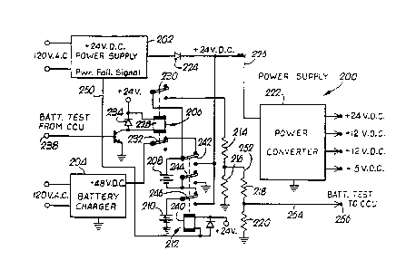
Fig. 2 illustrates power supply 200 which
supplies operating power to the various components
of system 30. Power supply 200 includes +24 V.D.C.
power supply 202, conventional battery charger 204,
battery test relay 206, 24 volt batteries 208 and
210, power failure relay 212, load resistors 214 and
216 ~each 25 ohm, 50 watt), test resistor 218 (51.1
K ohms), test resistor 220 (10.0 K ohms), and power
converter 222.
Conventional +24 V.D.C. power supply 202
receives input from a source of 120 V.A.C. and
delivers an output at +24 V.D.C. via blocking diode
224 and line 226 as input to power converter 222.
Power converter 222 provides output power
to the various components of system 30 at +24, +12,
-12, and +12 V.D.C. as shown. Converter 222 is
conventional in nature and preferably includes a
-- 10 --
~.". .. .... . . .. .... .. .
0 ~ 7 ~
1 D.C./D.C. converter (type PKA-2232P, not shown), to
supply power at +5 V.D.C. and also includes a pair
of regulators (type LN320T-12, not shown) to respec-
tively supply power at +12 and -12 V.D.C.
- 5 Test relay 206 includes coil 228 operable
at +24 V.D.C., and contacts 230 and 232. One side
of coil 228 is connected to the cathode of suppres-
sion diode 234 and +24 V.D.C. The other side of
coil 228 is connected to the anode of diode 234 and
to the collector of transistor 236. The emitter of
transistor 236 is connected to ground as shown and
the base is connected to terminal 238.
When terminal 238 receives a logic high
(+5 V.D.C.) signal from CCU 300, transistor 236
conducts in order to energize coil 228 and to oper-
ate contacts 230 and 232 to place batteries 208, 210
under load as will be explained further hereinbelow.
Conventional battery charger 204 receives
an input from a source of 120 V.D.C. and provides an
output at +48 V.D.C. to contact 232 as shown in Fig.
2.
Conventional electromechanical power
failure relay 212 includes coil 240 and contacts
242, 244, and 246.
The positive side of battery 208 is con-
nected to contact 230 of test relay 206 and also to
contact 242 of power failure relay 212. The nega-
tive side of battery 208 is connected to contacts
244 and 246 of power failure relay 212 as shown.
The positive terminal of battery 210 is connected to
contact 246 and the negative side is connected to
ground as shown.
One side of coil 240 is connected to the
cathode of suppression diode 248 and to +24 V.D.C.
The other side of coil 240 is connected to the anode
-- 11 -
7 ~
1 of diode 248 and via line 250 to the power failure
signal terminal of power supply 202.
Normally, batteries 208 and 210 are off
line and receive charging current from battery
- 5 charger 204 by way of contact 232 and contact 242 to
battery 208 and also by way of contact 246 to bat-
tery 210.
In the event of power failure, power
supply 202 internally couples line 250 to ground
which energizes coil 240. This in turn operates
contacts 242-246. When such occurs, the positive
output from each battery 208, 210 is connected via
contacts 242 and 246 respectively to line 226 in
order to supply power to power converter 222.
Contact 244 when operated by coil 240 connects the
negative side of battery 208 to ground as shown.
In the event of a battery test signal from
CCU 300 which energizes coil 228 as explained above,
contact 232 of test relay 206 takes battery charger
204 off line, that is, disconnects it from batteries
208, 210 and in turn connects the positive side of
battery 208 by way of contact 30 to one side of
resistor 214. Resistors 214 and 216 are connected
in series as shown and with test relay 206 actuated,
place a S0 ohm load on batteries 208, 210.
Resistors 214 and 216 are interconnected
by line 252 which is in turn connected to one side
of resistor 218 which together with resistor 220
form another voltage divider network. Line 254
interconnects resistors 218 and 220 and additionally
connects to output terminal 256. With test relay
206 actuated and batteries 208 and 210 under load, a
nominal voltage of 1.96 V.D.C. is produced at termi-
nal 256 which is read and analyzed by CCU 300 in
order to determine whether the voltage on batteries
0 7 ~
1 208, 210 is maintained while under load. Prefer-
ably, the battery test is conducted once a week for
one hour at the end of which the battery voltage as
represented by the voltage on terminal 256 is read
- 5 and analyzed by CCU 300. If the battery voltage is
below a predetermined limit, a trouble indication is
generated. As an alternative battery test, the
batteries can be placed under load until their
voltage falls below a certain level with the time
interval for this to occur being an indication of
battery capacity.
Fig. 3 illustrates central control unit
300 which includes microprocessor 302 (Intel 8097)
including a conventional oscillator circuit (not
shown) generating clock signals at 11.0592 mega-
hertz. CCU 300 also includes serial port interface
304, real time clock 306, watchdog and audible alarm
circuit 308, input/output ~I~O) controller 310,
input driver 312, output driver 314, memory decode
logic circuit 316, program read only memory ~ROM)
318, system random access memory ~RAM) 320, non-
volatile random access memory ~NVRAM) 322, and
nonvolatile random access memory (NVRAM) 324.
Components 302-324 are conventional in nature and
conventionally interconnected.
Microprocessor 302 receives the voltage
input representative of the test voltage on batter-
ies 208, 210 as discussed above in connection with
power supply 200 from terminal 256 at terminal P0Ø
By monitoring the voltage received thereby, micro-
processor 302 through its operating program deter-
mines whether the battery test voltage is within
predetermined limits. If not, microprocessor 302
stores this information in NVRAM 76 and announces
- 13 -
,. . ,. , . _ . . . . . .. .. .... .
l~Oq7.
1 and displays this condition by way of display module
1100.
Microprocessor 302 sends and receives
signals via I/O controller 84 to power supply 16.
- 5 One of these signals is the battery test signal
initiated at terminal 238 (Fig. 2). Additionally,
microcomputer 302 receives signals indicative of AC
power failure, blown fuses, and the like (not
shown).
Serial port interface 304 is coupled with
microprocessor 302 for transfer of data to and from
remote locations. For example, interface 304 can be
used to remotely monitor the operation of system 30
by receiving information concerning the operating
history from NVRAM 322 indicating any troubles or
alarms. Additionally, interface 304 can be used to
change the program or system configuration as stored
in program ROM 318 or NVRAM 324 from remote loca-
tion. Interface 304 can also provide information to
a graphic annunciator (not shown) for illustrating
the location of an alarm or trouble condition.
Real time clock 306 provides real time
information to display module 1100 and to history
NVRAM 322 to store the real time of a trouble or
alarm event.
Watchdog and audible alarm circuit 308 is
preferably included to reset microprocessor 302 in
the event it improperly executes its program. As is
conventional, the program includes code to periodic-
ally strobe and thus reset the watchdog before it
times out and resets microprocessor 302. An audible
alarm is included to sound in the event the watchdog
times out.
I/O controller 310 decodes and controls
the input and output functions of microprocessor 302
- 14 -
. .",. . . , , ,~ .. .... .. ...
~ 13~17~
l to write to or read from, and enable, external
devices via input driver 312 and output driver 314
as well as to power supply 200. Drivers 312 and 314
are operably coupled with input/output (I/O) bus
- 5 328.
Microprocessor 302 also generates and
delivers pulse voltage signals to control detector
module 600 via output terminal 326.
Microprocessor 302 writes to, reads from,
and enables its auxilliary memory devices 318-324 by
way of conventional memory decode logic 316.
Program ROM 318 includes a capacity of 64
K bytes and stores the operating program for micro-
processor 302.
System RAM 320 preferably includes 16 K
bytes of memory capacity for storing data used
during operation.
NVRAM 322 stores history information re-
garding the operation of system 30. With its pre-
ferred 16 K bytes of memory capacity, NVRAM 322
stores information concerning the past 256 events,
either troubles or alarms, of system 30 with suffi-
cient detail to display on display module 1100 the
nature of events including the real time and date at
which each occurred.
NVRAM 324 with 64 K bytes of preferred
memory stores information concerning the configura-
tion of system 30. More particularly, NVRAM 322 in-
cludes information concerning the definition of the
fire protection zones such as cross-zone, verified
zone, building protection scheme or the like. In
addition, NVRAM 324 stores the sensitivity data for
each detector, the type and number of detectors
included in system 30, the specifications for the
test limits of the detectors, and the type and
- 15 -
~3~07 .-~
1 location of external devices, and the number of
connector and detector modules.
Fig. 4 illustrates connector module 20
which is typical of a plurality of connector modules
- 5 which may be coupled to CCU 300 by I/O bus 328.
Connector module 400 provides an innerface with
external devices by means of which CCU 300 can
interact with those devices.
Module 400 includes connector decoder 402
operably coupled with I/O bus 328, slot decoder 106
operably coupled with decoder 402 and with connector
slots 1, 2, 3, 4, 5, 6, 7, 8, as illustrated. Each
slot 1-8 provides the physical connection with the
external device with each designed to connect with
an input/output module. For connection with detec-
tor module 600, two adjacent slots are required.
In operation, decoder 402 monitors bus 328
and when the correct address is received for the
particular connector module 400, allows slot decoder
404 to enable the appropriate slots so that the
external device can seize bus 328 for reading or
writing information.
Fig. 5 illustrates I/O module 500 connect-
ed via slot 7 of connector module 20 which includes
output section S01 and input section 502. Sections
S01, 502 are designed to receive respectively an
input from a remote device such as a manual pull
station for indicating a fire, or to provide an
output in order to actuate a remote device such as a
halon gas release system. Advantageously, module
500 can be configured for two outputs thereby form-
ing a dual output module or for two inputs thereby
forming a dual input module if desired. Module 500
with both an input and an output is illustrated so
- 16 -
,. .~..... .... . .. . . ... _. . . . .,~ .. . . . . ,." ,
13~1~Q7~;
that the preferred embodiment of both can be de-
scribed.
Output section 502 includes verification
circuit 503, latch 504, output circuit 505, and
input data buffer 506.
Verification circuit 503 interposes D-type
flip-flop 507 between data line D7 of I/O bus 328
and pin 3 of latch 504 so that two write signals
must be received at terminal 508 and two enable
signals at terminal 509 before data is clocked
through latch 504 as output via pin 20 thereof.
Verification circuit 503 thereby requires that two
command signals be received from CCU 300 before an
output device connected to output section 501 can be
actuated.
In operation, a logic low write signal
received via terminal 508 and a logic low enable
signal received via terminal 509 provide respective
inputs to NOR 510. With both inputs low, the output
from NOR 510 goes high to clock terminal CLK of
flip-flop 507. Line D7 is connected to data termi-
nal D of flip-flop 507 and the signal on terminal
CLK clocks through data to output terminal Q.
Output terminal Q is connected to one side
of resistor 511 (lM ohms). The other side of resis-
tor 511 is connected to one side of capacitor 512 (1
u.F.) the other side of which is grounded, to one
side of resistor 513 (100 ohms), and to the positive
input terminal of comparator 514. The negative
input terminal of comparator 514 is biased at +2.4
V.D.C.
When terminal Q of flip-flop 502 goes high
at +5 V.D.C., this exceeds the reference voltage of
+2.4 V.D.C. on comparator 514 and its output is
thereby pulled high to pin 3 of latch 504. Capaci-
- 17 -
0 7 ~i
1 tor 512 slows the voltage rise to the positive input
terminal of comparator 514 so that its output does
not go high until after the strobe signal is receiv-
ed at pin 2 of latch 504 from NOR 510. Thus, the
- 5 first strobe signal received at pin 2 of latch 504
clocks through data at logic low (0 V.D.C.) from pin
3 to pin 20 and the output at pin 20 which is in-
verted remains at +24 V.D.C. and prevents actuation
of the external device connected to output section
501.
When a second write signal and a second
enable signal are received at terminals 508 and 509
respectively, a logic high signal is already present
on latch pin 3 and the output at pin 20 is pulled
low to 0 V.D.C. The output from NOR 510 is also
connected to one side of resistor 515 (10 K ohms),
the other side of which is connected to ground as
shown.
Data lines 0-6 of I/O bus 328 connect
directly to latch 504 as shown.
Flip-flop output terminal ~ is connected
to the gate of junction field effect transistor
(FET~ 516, the drain of which is grounded. The
source terminal of FET 516 is connected to the other
side of resistor 513.
In operation, when flip-flop 507 clocks
through data at logic low, ~ goes high which quickly
enables FET 516 to pull the voltage low on the
positive input terminal of comparator 514.
Module 500 receives reset signals from CCU
300 via terminal 517 which is connected to an input
NOR 518 which also receives the enable signal from
terminal 509. In the event a reset and enable
signal are received, the output from NOR 518 is
pulled high through resistor 519 (2.2 K ohms) the
- 18 -
~4~7~
l other side of which is connected to +5 V.D.C. as
shown. NOR 518 output is also connected to reset
terminal pin 1 of latch 504 and to the gate of
junction field effect transistor (FET) 502. The
source terminal of FET 520 is grounded and the drain
terminal is connected to the inverted reset terminal
of flip-flop 507 and to one side of pull-up resistor
521 (10 K ohms) the other side of which is connected
to +5 V.D.C. as shown. Capacitor 522 (0.1 u.F.) is
connected in parallel with FET 520 as shown.
When transistor 520 receives a reset
signal from NOR 518, the input to reset terminal R
of flip-flop 507 is pulled low to reset it.
Latch 504 (type UCN5801) latches and
inverts the data received via I/O bus 328 and data
line D7 by way of verification circuit 503. Pins 17
and 13 are connected respectively to light emitting
diode-units (type 560-0103) 523 and 524 the other
sides of which are connected to +3 V.D.C. as shown
which is also connected to one side of capacitor 525
(10 u.F.) the other side of which is grounded.
Output circuit 505 is designed to couple
with an external polarized output device for super-
vised Class A wiring. Output 527 circuit 505 in-
cludes output relay 526 having coil 527 and contacts
528 and 529, "~arch" time relay 530 having coil 531
and contacts 532 and 533, and Class A relay 534
having coil 535 and contacts 536 and 537.
During normal operation when no output
device is actuated, latch pin 20 is high at +24
V.D.C. preventing energizing of output relay 526.
Supervisory current flows via line 538 through
contact 528, contact 532, line 198, and transient
suppression device 539 (type DSS310) to output
terminal 540. Current flow continues from terminal
-- 19 --
.,. , .,, , ,~ . , , . . . j, ,~ .. .
13 i~075
1 540 through the polarzied circuitry of the output
device (not shown) and back to output terminal 541.
The return current flows therefrom through fuse 542
(typically 375 milliamps), contact 533, contact 529,
- 5 and resistor 543 (680 ohms) to ground.
Capacitor 544 (0.1 u.F.) intercouples one
side of device 539 with contacts 528 and 532, and
capacitor 545 (0.1 u.F.) intercouples terminal 540
with one side of fuse 542 as shown. In addition,
capacitor 546 intercouples one side of contact 533
with the other side thereof as shown. Capacitor 547
(10 u.F.) is connected to ground and in parallel
with resistor 543.
output circuit 505 provides supervisory
current as part of a Class A wiring system in order
to detect a short or open circuit in the wiring
leading to the remote output device to enhance
reliability. The supervisory current flow through
resistor 543 provides a voltage in the range of 2.8
to 4.0 V.D.C. which is connected to the negative
input terminal of short circuit comparator 548. The
positive input terminal of comparator 548 is con-
nected to reference at 5.6 V.D.C. In the event of a
short circuit between the wires leading to remote
output device which in effect shorts terminals 540
and 541, the supervisory current increases to pro-
duce a voltage to the negative input terminal of
comparator 548 which exceeds the reference voltage
at +5.6 V.D.C. When this occurs, the output from
comparator 548 goes low to pin 8 of data input
buffer 506. The data from pin 8 is read on data
line D2 of I/O bus 328. Pull up voltage is provided
to the output of comparator 54~ at +5 V.D.C. via
resistor 549 (2.2 K ohms).
- 20 -
,, ~. " ....... . ...... .
~' 13'1~07~
The voltage drop across resistor 543 is
also provided to the positive input terminal of open
circuit comparator 550, the negative input terminal
of which is connected to reference at +2.4 V.D.C.
- 5 In the event of an open circuit in the lines leading
to the remote output device, the voltage on resistor
543, which is normally 2.8 to 4.0 V.D.C., falls
below the level of the reference voltage of +2.4
V.D.C. and the output from comparator 550 goes low
to pin 7 of buffer 506. This data is read via data
line D3 of I/O bus 328. Pull up voltage to the
output of comparator 550 is provided at +5 V.D.C.
via resistor 551 (2.2 K).
When a short or open circuit occurs in the
wiring leading to the output device, CCU 300 reads
the data indicative thereof on I/O bus 328 and
actuates Class A relay 534 by writing data on data
line D5 to latch 504 which cau,ses pin 18 to go low
and sink current thereby energizing coil 535. When
this occurs, contacts 536 and 537 operate in order
~ to connect with output terminals 552 and 553 respec-
tively. Terminals 552 and 553 are respectively con-
nected to lines running parallel to the lines con-
nected to terminals 540 and 541 to the remote output
device. In others words, when a short circuit or
open circuit occurs on the lines connected to termi-
nals 540 and 541, Class A relay 534 switches to the
parallel set of wires connected to terminals 552 and
543 respectively.
In the event two valid output command
signals are written to latch 504, pin 20 thereof
sinks current in order to energize output relay 526.
When this occurs, contact 529 operates in order to
connect with +24 V.D.C. and contact 528 operates to
connect with ground as shown. With this arrange-
- 21 -
13'101J7~
1 ment, operating current then flows outwardly through
terminal S41 ~or terminal 553 if relay 534 has been
energized) through the external device for actuation
thereof and in through terminal 540 (or terminal 552
- 5 if relay 534 is energized) and through contact 528
to ground. This actuates the external device in a
current flow direction opposite to that of the
supervisory current.
March time relay 530, when actuated by CCU
300 via data line D6 and latch 504 pin 19, prevents
all output through terminals 540, 541, 552 and 553
and is preferably used to "pulse" the output when
the output device is an audible alarm. The audible
alarm can be pulsed at different rates depending on
the type alarm situation existing becoming more
rapid as a suppressant release time nears, and
finally continous when release occurs.
Input section 502 which also uses data
buffer 506 reads an input from a remote device such
as a manual pull station. Input section 502 also
provides for supervisory current to detect short or
open circuits and Class A wiring control similar to
that of output section 501.
Supervisory current is produced by apply-
ing +24 V.D.C. to current limiting resistor 554 (1 K
ohms) which flows therefrom transient suppression
device 555 (type DSS310) and to terminal 556. The
supervisory current then flows through the remote
polarized input device and in through terminal 557,
fuse 558 (typically 375 milliamps), and resistor 559
(200 ohms) to ground. Capacitor 560 (0.1 u.F.)
intercouples terminal 556 and one side of fuse 558
as shown. Capacitor 561 (10 u.F.) is connected to
ground and in parallel with resistor 559 as shown.
- 22 -
~' 13~)37~
1 The voltage drop across resistor 559 is
provided to the negative input terminal of short
circuit comparator 562, the positive input terminal
of which is connected to reference voltage at +5.6
V.D.C. as shown. As with output section 501, if a
short circuit occurs in the lines leading to the
remote input device, the supervisory current flow
increases and produces a voltage drop through resis-
tor 559 exceeding the reference voltage at +5.6
V.D.C. Comparator 562 output then sinks current and
provides a logic low signal to buffer pin 4 which is
read on data line D1.
Resistor 559 is also connected to the
positive input terminal of open circuit comparator
563, the negative term;nal of comparator 276 is
connected to reference voltage at +2.4 V.D.C. as
shown. In the event an open circuit occurs in the
lines to the remote input device, the voltage on
resistor 559 falls below the reference voltage
level, and the output from comparator 563 goes low
to pin 3 of buffer 506 which is read on data line
D0. Pull-up voltage is supplied to the output of
comparator 562 at +5 V.D.C. via resistor 564 (2.2 K
ohms). Similarly, pull-up voltage is supplied at +5
V.D.C. the output of comparator 563 via resistor 565
(2.2 K ohms).
In the event a short or open circuit
occurs in the lines leading to the remote input
device, CCU 300 reads this information from buffer
506. CCU 300 is operable to write data to latch 504
which causes pin 14 thereof to sink current in order
to energize coil 566 and thereby Class A relay 567
from a source at +24 V.D.C. as shown. with relay
567 energized, contact 568 thereof operates to
intercouple terminal 556 with terminal 569 and to
- 23 -
i~O~75
l operate contact 570 to intercouple terminal 557 with
terminal 571. Resistor 572 (1.5 K ohms) intercoupl-
es terminals 569 and S71.
The preferred input devices coupled to
terminals 556, 557 include normally closed switches
used as so-called "abort switches" to prevent a fire
suppressant release condition and including an
end-of-line resistor in parallel with the abort
switches. An abort switch is active when open which
creates an electrically open circuit condition as
detected by comparator 563. The system configura-
tion defines the reaction to this open circuit
condition; and when the configuration defines termi-
nals 556, 557 as being coupled with normally closed
abort switches, CCU 300 reads an open circuit indi-
cation from comparator 563 as an active abort switch
and not as an open circuit.
The preferred input devices coupled with
terminals 556, 557 also include parallel normally
open switches with a parallel end-of-line resistor
which are used for manual pull stations to initiate
an alarm situation. Activation of a manual pull
station closes the switch which simulates an elec-
trically short circuit condition which is detected
by comparator 562. When the system configuration
defines terminals 556, 557 as being coupled with
normally open ~anual pull station switches, CCU 300
reads a short circuit condition from comparator 562
as an active manual pull station and not as a short
circuit.
A read command for buffer 506 is received
from CCU 300 at terminal 573 which is connected as
one input to NOR 574, the other input to which is
received from enable terminal 509. The output from
NOR 574 is connected to both inputs of NOR 575, the
- 24 -
7 5
1 output of which connects with inverting input pin 1
of buffer 506.
In the event a read signal at logic low is
received at terminal 573 along with a logic low
- 5 enable signal at terminal 509, the output from NOR
574 goes high, the output from NOR 575 goes low, and
buffer 506 seizes I/O bus 328.
Fig. 6 illustrates detector module 600
which controls detector loop 34 by providing the
appropriate voltage pulses to poll the individual
detectors and to receive the data therefrom. Module
600 includes detector pulse voltage control circuit
700 (Fig. 7), Class A wiring control circuit 800
(Fig. 8~, signal detector circuit 900 (Fig. 9), and
quiescent current null control circuit 1000 (Fig.
10). The output from detector pulse voltage control
700 connects to Class A wiring control 800 via line
602 and to one side of current limiting resistor 604
(221 K ohms). The other side of resistor 604 con-
nects to signal detector 900 and Q. current null
control 1000 via terminal 606.
Fig. 7 illustrates detector pulse voltage
control 700 which provides operating power to detec-
tor loop 34 by providing a regulated output voltage
at 26.5 V.D.C., and which provides voltage pulses at
38.5 V.D.C. in order to sequentially poll and reset
the detectors and to actuate a test, light-emitting
diode in each detector.
Circuit 700 receives input voltage at +24
V.D.C. as an input to conventional triangle wave
oscillator 702 providing a triangle wave at 24 volts
peak-to-peak. The output from generator 702 con-
nects to conventional voltage doubler 704 which in
turn provides an increased output at about 40-45
V.D.C. to pin 3 of conventional voltage regulator
- 25 -
7 S
l 706 (type LM317T~. Regulator 706 provides a regu-
lated steady state output at pin 2 thereof at 26.5
V.D.C. The regulated output from pin 2 connects to
one side of output load sensing resistor 708 (10
- 5 ohms). The other side of resistor 708 is coupled
with line 602 and output terminal 711 and thereby
detectors 36 via circuit 800, the cathode of voltage
limiting Zener diode 712 (type P6KE), the anode of
which is grounded as shown, and resistor 604.
Regulator 706 receives an adjusting input
at pin 1 thereof from regulator section 714 which
provides the adjusting input to regulator 706 in
order to cause the voltage pulses on the output
thereof.
Regulator section 714 receives an "on"
signal at logic high (+5 V.D.C.) directly from CCU
300 at terminal 716. The on signal is then inverted
by inverter 71a which provides,a logic low output to
one side of pull down resistor 720 (5.1 K ohms) the
other side of which is grounded, to the gate of
field effect transistor ( FET) 722, and to output
terminal 724 which provides feedback directly to CCU
300 indicating that the "on" signal has been receiv-
ed. The drain terminal of FET 722 is connected via
line 350 to pin 1 of regulator 706 and the source
terminal thereof is grounded.
With the gate of FET 722 low, FET 722 is
off, and resistor 725 (253 ohms) provides feedback
voltage from the output of regulator 706 to pin 1
thereof which boosts the output. When the signal is
absent from terminal 716 (i.e., at logic low), FET
722 is on which in turn shuts off the output at pin
2 thereof.
When FET 722 is turned off the output from
regulator 706 begins to rise because of the feedback
- 26 -
1 3 ~ 7 ~
1 provided by feedback resistor 72S (243 ohms). The
feedback voltage on regulator pin 1 is limited by
the series-coupled network of potentiometer 728 ~1.0
K ohms), resistor 730 (4.3 K ohms), and resistor
- 5 (2.32 K ohms) connected to ground which allows the
output of regulator 706 to rise to 38.5 V.D.C.
A logic low clock pulse received from CCU
300 at terminal 734 is inverted by inverter 736
which is conveyed via current limiting resistor 738
(10 K ohms) to the base of transistor 740, the
emitter of which is grounded and the collector of
which is connected to one side of resistor 732 as
shown. The low going pulse at terminal 734 turns on
transistor 740 and bypasses resistor 732 to ground
which in turn lowers the feedback voltage to regula-
tor pin 1 and lowers its output to 25.5 V.D.C.
In this way, CCU 300 toggles the output of
regulator 706 between 26.5 and, 38.5 V.D.C. by pro-
viding respective high at low signals at terminal
734.
Fig. 8 illustrates Class A wiring control
800. Line 602 from circuit 700 supplies the operat-
ing power and voltage pulses to one side of each
detector 38 in loop 34. The other side of each
detector is connected via line 702 to ground as
shown. Class A wires 704 and 706 are provided in
parallel with lines 602 and 702 respectively in
order to improve the reliability of loop 34 in the
event of a short or open circuit between or in lines
602 and 702.
As will be discussed further hereinbelow,
signal detector circuit 900 (Fig. 9) monitors the
magnitude of the current flow through detectors 38
in loop 34 and from the information obtained thereby
determines whether a short or open circuit exists.
- 27 -
~3~7.~
1 If a short or open occurs, CCU 300 pro-
vides a logic high signal at terminal 708 to one
side of pull down resistor 710 (511 K ohms) the
other side of which is grounded, and to the gate of
- 5 FET 712. The source terminal of FET 712 is grounded
and the drain terminal is connected to the anode of
transient suppression diode 714 and to one side of
coil 716 of Class A relay 718 having contacts 720
and 722 connected as shown. The cathode of diode
714 and the other side of coil 716 are connected to
+24 V.D.C. Normally open contact 720 intercouples
line 602 with line 704, and normally open contact
722 intercouples line 706 with ground.
With a logic high signal at terminal 708,
FET 712 conducts and thereby energizes coil 716 to
close contacts 720 and 722. This in turn places
lines 704 and 706 in service in order to keep detec-
tors 38 in service. ,
As will be explained further hereinbelow,
detectors 36 each draw a normal operating current
the total of which is a quiescent current flow
through resistor 708 (Fig. 7) and then through line
602 to detectors 36. This current flow produces a
voltage drop through resistor 708 such that the
total of the voltage drop across resistor 708 and
detector loop 34 equals 26.5 V.D.C. which is the
voltage supplied as output from regulator 706.
Detectors 36 sequentially convey information by
adjusting the current flow therethrough. Signal
detector circuit 900 (Fig. 9) monitors the voltage
drop across loop 34 by monitoring the voltage at
terminal 606 which is connected to line 602 and the
detector loop by way of and resistor 604 (Figs. 6
and 7). Thus, the voltage signal at terminal 606 is
representative of the various current magnitudes
- 28 -
". , , ~, .~ _ ,,, . ,, . " , . . . .. .. .
l~Q07.~i
1 flowing through detector loop 34 which are in turn
representative of the particular environmental
condition parameter being measured, that is, is
smoke obscuration.
Fig. 9 illustrates signal detector circuit
900. In general, circuit 900 converts the voltage
monitored at terminal 606 to a digital value for
transmission to CCU 300. More specifically, circuit
900 has two functions. First, it monitors the
quiescent current flow through loop 34 as a quies-
cent voltage at terminal 606 in order to provide a
digital voltage representative thereof to CCU 300.
CCU 300 in turn provides a digital signal to Q
current null control circuit 1000 (Fig. 10) which
produces an output voltage at terminal 606 to offset
the quiescent voltage and thereby compensate for the
quiescent current. After Q. current null control
circuit 1000 has compensated for the quiescent
current flow, signal detector circuit 900 converts
the voltage signals representative of the various
current flow magnitudes through detector loop 34
into digital form for processing by CCU 300.
Signal detector 900 receives the voltage
from terminal 606 at current-to-voltage, one-to-one
amplifier 902 at the positive input terminal there-
of. The output from amplifier 902 connects with the
negative input terminal thereof, with one side of
resistor 904 ~5.5 K ohms) the other side of which is
connected to ground, and with one side of resistor
906 (2.7 K ohms). The other side of resistor con-
nects with one side of capacitor 90~ (0.001 u.F.),
one side of resistor 910 (27.4 K ohms) and to the
negative input terminal of amplifier 912 (type
LF347N). The positive input terminal to amplifier
- 29 -
007~
1 912 is connected to ground as shown and receives
supply voltage at +12 and -12 V.D.C.
Amplifier 912 output connects with the
other side of capacitor 908, the other side of
- 5 resistor 910, one side of resistor 914 (27.4 K
ohms), and to the positive input terminal of voltage
limiting amplifier 916.
Amplifier 912 provides ten-to-one amplifi-
cation of the input voltage with an output span from
-12 V.D.C. to +12 V.D.C. Amplifier 916 and the
circuitry associated therewith receive the amplified
voltage from amplifier 912 and convert to a span
from 0 to +5 V.D.C. as suitable input to the analog-
to-digital converter.
Amplifier 916 output connects with the
cathode of diode 918, the anode of which is connect-
ed to the negative input terminal of amplifier 916,
to one side of resistor 920 (5.1 K ohms) and to the
positive input terminal of voltage limiting amplifi-
er 922. The other side of resistor 920 connects
with +5 V.D.C. as shown. With this arrangement, the
output from amplifier 918 is limited to a maximum
positive voltage of +5 V.D.C. and amplifier 922
limits the low voltage to 0 volts.
The output from amplifier 922 connects
with the anode of diode 924, the cathode of which is
connected to the negative input terminal of ampli-
fier 922, to one side of pull down resistor 926 (5.1
K ohms) the other side of which is connected to
ground as shown, and to terminal CHl of analog-to-
digital (A/D) converter 928. A/D 928 provides a
digital output representative of the quiescent
current flow on I/O bus 328 to CCU 300.
The remaining portions of signal detector
circuit 900 beginning with resistor 914 integrate
- 30 -
~340~7 ~
1 voltage levels representative of the successive
current levels in detector loop 34 for reception at
terminal CH2 of A/D 928.
The other side of resistor 914 connects
with to the negative input terminal of one-to-one
buffer amplifier 930 and with-one side of resistor
932 ~27.4 K ohms). The positive input terminal of
amplifier 930 is connected to ground as shown and
the output thereof is connected to the other side of
resistor 932, to one side of pull down resistor 934
(5.1 K ohms), and to pin 3 of unijunction device 936
(type DG201).
Device 936 includes an internal unijunc-
tion transistor and inverter as shown. Pin 1 of
device 936 receives an inverted input from terminal
938, inverter 940. One side of pull up resistor 942
(10 K ohms) connects with terminal 938 and the other
side is connected to +S V.D.C.
CCU 300 provides a logic high "integrate"
signal at terminal 938 which is inverted by inverter
940 to supply a logic low input at pin 1 of device
936. This in turn enables device 936 to pass the
input from pin 3 to output pin 2.
Device 936 output at pin 2 is connected to
one side of re~istor 944 (10.0 K ohms). The other
side of resistor 944 is connected to the negative
input terminal of integrator amplifier 946, to one
side of integrator capacitor 948 (0.1 u.F.) and to
pin 6 of device 950 which is identical and included
on the same se~iconductor chip as device 936. The
positive input terminal of amplifier 946 is connect-
ed to ground as shown and the output thereof is
connected to one side of pull down resistor 952 (S.l
K ohms) the other side of which is grounded, to the
positive input terminal of voltage limiting amplifi-
- 31 -
,. . ~. .. . . . .
0075
1 er 954, to one side of resistor 956 (270 ohms), and
to pin 7 of device 950. Capacitor 948 and resistor
956 are interconnected as shown.
CCU 300 provides the logic high integrate
- 5 signal at terminal 938 for one millisecond during
which time amplifier 946 and capacitor 948 integrate
this signal. At the end of one millisecond, the
integrate signal goes off and the integrated voltage
as output from amplifier 946 is held for conversion
by A/D 928.
After conversion, CCU 300 provides a logic
high "dump" signal at terminal 958 and to inverter
960 which inverts the signal to logic low at pin 8
of device 950. Device 950 is thereby enabled and
discharges capacitor 948 through resistor 956 to
reset the circuit for another integration cycle.
Pull up voltage is provided at +5 V.D.C. to terminal
958 by way of resistor 962 (lO K ohms).
The output from integrator amplifier 946
is received at the positive input terminal of limit-
ing amplifier 954. The output therefrom is connect-
ed to the cathode of diode 964, the anode of which
is connected to the negative input terminal of
amplifier 954 and to one side of pull up resistor
966 (5.1 K ohms) the other side of which is connect-
ed to +5 V.D.C. as shown. As with amplifier 916,
amplifier 954 limits the integrator voltage signal
to +5 V.D.C.
The anode of diode 964 is also connected
to the positive input terminal of limiting amplifier
968 the output of which is connected to the anode of
diode 970. The cathode of diode 970 is connected to
one side of pull down resistor 972 (5.1 K ohms) the
other side of which is grounded, and to terminal CH2
- 32 -
~ 3 ~ 7 .5
1 of A/D 928. Amplifier 968 limits the lower voltage
of the integrated voltage signal to 0 volts.
A/D 928 receives a logic low read signal
from CCU 300 at terminal 974 which is received at
terminal RD of A/D 928. A logic low write signal is
received from CCU 300 at tèrminal 976 which is
received at A/D terminal ~.
CCU 300 produces a logic low enable signal
at terminal 978 as an input to OR 980 which receives
its other input from terminal 982 as a logic low
data signal from I/O bus 328. The output from OR
980 is connected to terminal ~ of A/D 928. A/D 928
also receives an interrupt signal at terminal
from CCU 300 at terminal 984 which is connected to
data line 0 of I/O bus 328. A/D 928 terminal 7 is
connected to ground as shown and vREF is connected
to 4.0 V.D.C.
As discussed above, C,CU 300 reads a digi-
tal value on I/O bus 32B representative of the
quiescent voltage on terminal 606 as produced by A/D
928 when reading CHl. CCU 300 also reads a digital
value representative of the current magnitudes on
detector loop 34 as integrated by capacitor 948 and
supplied to A/D 928 terminal CH2.
Fig. 10 illustrates quiescent null control
circuit 1000 which compensates for the quiescent
current in detector loop 34 at terminal 606. CCU
300, in response to the digital values representa-
tive of the quiescent current received by signal
detector 900, sends a corresponding compensating
digital value by way of I/O bus 328 to digital-to-
analog converter (DAC) 1002 (type DAC1230). In
response, DAC 1002 produces an analog output at DAC
terminals IOl and IO2 which are connected to the
respective negative and positive input terminals of
- 33 -
() 7 5
1 current-to-voltage amplifier 1004 (type LF347N).
Terminal IO1 is also coupled with one side of capac-
itor 1006 (22 p.f.) and to one side of pull down
resistor 1008 (5.5 K ohms) the other side of which
is grounded. Terminal IO2 is also grounded.
The output from amplifier 1004 is connect-
ed to the other side of capacitor 1006, to DAC
terminal RFB, and to one side of output resistor
1010 (1.82 K ohms). The other side of resistor 1010
connects to one side of resistor 1012 (15.4 K ohms)
the other side of which is grounded, to one side of
resistor 1014 (5.11 K ohms) the other side of which
is connected to -12 V.D.C. as shown, and to the
positive input terminal of amplifier 1016 ~type
LF347N).
The output voltages produced by amplifier
1004 ranges between -2.90 and -5.34 V.D.C. as input
to the positive input terminal of amplifier 1016.
The output from amplifier 1016 is connected to one
side of pull down resistor 1018 (10 K ohms~ the
other side of which is grounded, and to one side of
resistor 1020 (330 ohms).
The other side of resistor 1020 is con-
nected to the base of transistor 1022 Itype 2N4123).
The collector of transistor 1022 is connected to one
side of resistor 1024 (8.2 K ohms) the other side of
which is connected to terminal 606 and the emitter
is connected to the negative input terminal of
amplifier 1016 and to one side of resistor 1026
~68.1 K ohms), the other side of which is connected
-12 V. D.C. as shown.
Reference voltage is provided to DAC 1002
using the voltage divider network composed of resis-
tor 1028 (1.1 K ohms) one side of which is connected
to +4 V.D.C. and the other side of which is connect-
- 34 -
0075
1 ed to one side of resistor 1030 (10.0 K ohms~ which
is grounded as shown. The junction between resis-
tors 1028 and 1030 is connected to the positive
input terminal of one-to-one amplifier 1032 (type
- 5 LF347N). The output of amplifier 572 provides
reference voltage at +3.60 V.D.C. to terminal VREF
of DAC 1002 and which also provides feedback to the
negative input terminal of amplifier 1032.
CCU 300 provides control signals to DAC
1002 which include a logic low enable signal provid-
ed at terminal 1034 as one input to OR 1036. The
other input to OR 1036 is data line D0 from I/O bus
328. The output from OR 1036 is connected to termi-
nal CS of DAC 1002.
Additionally, DAC 1002 also receives a
logic low write signal at terminal WR1 thereof from
CCU 300 via terminal 1038. Data line D1 is connect-
ed via line 584 to DAC terminal B1/B2.
In operation, amplifier 1016, transistor
1022, and the associated resistors comprise an ad-
justable current source the resulting effect of
which compensates for the quiescent current flow in
detector loop 34 by balancing the quiescent voltage
at terminal 602. As will be explained further
hereinbelow, CCU 300 performs successive iterations
of adjustment until the quiescent voltage is bal-
anced within predetermined limits.
Fiq. 11 illustrates display module 1100
which provides a liquid crystal display of alarm and
trouble conditions, locations of these conditions,
and other information concerning the operation of
system 30. Additionally, module 1100 provides the
interface for various membrane switches and also
illuminates certain LED's indicative of the status
of system 30.
- 35 -
oa7s
1 More particularly, module 1100 includes
microprocessor-based liquid crystal display (LCD)
1102 (type PWB-16230) which receives data from CCU
300 via I/O bus 328. CCU 300 also provides range
- 5 control inputs to LCD 1102 including a register
select signal from terminal 1104 provided to LCD
terminal RS. Additionally, CCU 300 provides read/
write signals via terminal 1106 to LCD terminal R~W.
An LCD enable signal is conveyed via terminal 1108
to LCD terminal EN. One side of pull down resistor
1100 (5.1 K ohms) is connected to terminal 1108 and
the other side is connected to ground.
LCD display 1102 provides an output at pin
15 to pin 2 of conventional LCD backlight 1112 in
order to sink current for illumination of the dis-
play. Pin 1 of backlight 1112 is connected to +5
V.D.C.
Module 1100 also provides for input buf-
fering of six membrane switches 1114 having the
functions as indicated in Fig. 11. Input buffering
is provided by device 1116 ~type 74C923) which is
intercoupled with membrane switches 1114 as shown.
Device 1116 is also coupled with I/O bus 328 for
delivering data indicative of which membrane switch
is depressed to CCU 300. Device 1116 receives an
enable signal from CCU 300 via terminal 1118 to
device terminal OE as shown. Device pin 6 connects
to one side of capacitor 1120 (0.1 u.F.) the other
side of which is grounded and device pin 7 connects
to capacitor 608 (1.0 u.F.) the other side of which
grounded. Device 1116 receives an interrupt signal
from CCU 300 via terminal 1124 at terminal DA.
Module 1100 also includes an output buffer
device 1124 to actuate four light emitting diodes
(LED's) 1126, 1128, 1130, and 1132 and a piezo-
- 36 -
, . . . . .... v . ~ ,, . . . . . ,.. ~.
t~g7~
1 electric buzzer 1134. Device 1124 (type 74LS373) is
connected to data lines D0-7 of I/O bus 328 as
shown. Data lines D1 and D3 are respectively coupl-
ed to one side of resistors 1136 and 1138 (2.2 K
ohms each) the other sides of which are connected to
+5 V.D.C. Data lines D0, 2, and 4 are respectively
coupled with one side of pull down resistors 1140,
1142 and 1144 (5.1 K ohms each) the other sides of
which are connected to ground as shown. Device 1124
receives a strobe signal from CCU 300 at device pin
11 terminal 1146.
Depending on the data received via data
bus 328, device 1124 is operable to provide an
output at pin 2 to one side of resistor 1148 (5.0
ohms) the other side of which is connected to the
base of transistor 1150. The emitter of transistor
1150 is connected to ground as shown and the collec-
tor is connected to pin 3 of backlight 1112 for
acutation thereof.
Pin S of device 1124 provides an output to
piezo buzzer 1134 which is also connected to +5
V.D.C. as shown.
Device pin 6 is connected to inverter 1152
which is in turn connected to the cathode of LED
1126. The anode of LED 1126 is connected to one
side of current limiting resistor 1154 (160 ohms)
the other side of which is connected to +5 V.D.C.
Device pin 9 connects to inverter 1156.
The output from inverter 1156 is connected to in-
verter 1158 and to the cathode of LED 1130. The
anode of LED 1130 is connected to one side of cur-
rent limiting resistor 1160 ~160 ohms) the other
side of which is connected to +5 V.D.C.
The output from inverter 1158 is connected
to the cathode of LED 1128 the anode of which is
- 37 -
, ~ ,. . . . ... ... . . .. . . .
r~ '
7.5
1 connected to one side of current limiting resistor
1162 (160 ohms). The other side of resistor 1162 is
connected to +S V.D.C.
Device pin 12 connects to the input of
- 5 inverter 1164 the output of which connects to the
cathode of LED 1132. The cathode of LED 1132 is
connected to one side of current limiting resistor
1166 (160 ohms) the other side of which is connected
to +5 V.D.C. as shown.
Depending upon the type of abnormality
experienced by system 30, the appropriate data is
transmitted via I/O bus 328 to actuate appropriate
LED' S 1126-1132. Such occurences also actuate piezo
buzzer 1134 which can be silenced by depressing the
"silence" membrane switch 1114 in which case LED
1132 is actuated and thereby illuminated, for ex-
ample.
The preferred detector 36 is manufactured
by Hochiki Kabushiki Kaisha of Tokyo, Japan type
ALA-E3 and is designed to detect smoke obscuration
as a percent per meter. As discussed above, detec-
tor module 600 supplies continuous operating power
at 26.5 V.D.C. CCU 300 in turn provides pulse
signals which are modified by detector module 24 to
provide voltage pulses up to 38.5 volts thereby
producing a pulse voltage rise of 12.0 volts.
As illustrated in Fig. 12, the voltage
pulses each last for 2 milliseconds and are normally
spaced apart by 12 milliseconds (that is, on a 14
millisecond cycle).
Each detector 36 is assigned a sequential
identification number and is designed to sense and
count the number of voltage pulses imposed on detec-
tor loop 34. When the number of pulses sensed
corresponds to the identity number of the individual
- 38 -
13~J~7~
l detector, that detector is then actuated to impose
sequential analog currents as data onto detector
loop 34. This data is in turn sensed by signal
detector circuit 600, converted into digital form,
~ 5 and transmitted to CCU 300.
During the 14 millisecond period between
the center of one voltage pulse and the center of
the next voltage pulse, the polled detector sends
seven analog current levels each lasting two milli-
seconds. These analog current levels called
"states" correspond to predetermined types of data.
For example, state I3 represents a reference current
level corresponding to the normal steady current
flow through the polled detector. State Is(n)
represents the sensed level of smoke obscuration as
a percent per foot. State I~ represents a predeter-
mined current level which indicates the type of
detector. For example, othe~ types of detectors
could be included such as ionization or temperature.
Each detector 36 also includes a test,
light-emitting diode (LED) which, when actuated,
places the detector in a test mode to provide a
reference illumination simulative of 4.5% per meter
smoke obscuration. When acutated, the data repre-
sentative of this reference obscuration is transmit-
ted as I5(t) in place of I5(n). The test LED's in
all the detectors are actuated by spacing out the
voltage pulses in order to provide two successive 16
millisecond gaps between voltage pulses rather than
the normal 12 ~illiseconds. That is to say, when a
detector senses two successive intervals of 16
milliseconds between voltage pulses, the detector
acutates its test LED. A subsequent single 16
millisecond interval causes the detector to deacti-
- 39 -
1~40~75
1 vate the test LED and thereby return to the normal
mode.
U.S. Patent Nos. 4,555,695 and 4,388,616,
which are hereby incorporated by reference explain
- 5 further details concerning detectors 36 and applica-
tions thereof.
System 30 is designed to handle up to 127
detectors 36 on a single detector loop 34. After
127 voltage pulses have been imposed on detector
loop 34 thereby polling all detectors 36, detector
module 600 as controlled by CCU 300 emits a single
14 millisecond pulse as illustrated in Fig. 12 which
resets to zero all of the internal detector count-
ers. Detectors 36 are then ready for the next
cycle.
II. Operating Program
Figs. 13A-21C illus,trate the computer
program flowchart for the pertinent portions of the
computer program for operating microprocessor 302
(Fig. 3) and thus system 30. In the preferred
system, microprocessor 302 is an Intel type 8097 and
the program is accordingly written in PLM which is a
high level language appropriate for the preferred
microprocessor. Those skilled in the art will
appreciate that the computer program as illustrated
in the flowcharts can be implemented in other lang-
uages as a matter of design choice and as appropri-
ate for a selected computer system which in addi-
tional to other types of microprocessors might
include a minicomputer or even a main frame. The
operating program is stored in program ROM 318.
Figs. 13A,B illustrate the subroutine
STARTUP/RESET. This subroutine is executed during
power up, whenever watchdog 308 times out and initi-
- 40 -
~ ~4~7~;
1 ates a reset, or when the reset membrane 1114 switch
is depressed.
The program enters STARTUP/RESET subrou-
tine at step 1302 which deactivates all of the input
or output modules 500 including the Class A relays
associated therewith. In addition, this step de-
activates LED's 1126-1132 tFig. 11) and the audible
piezo buzzer 1134. At this time CCU 300 also acti-
vates LCD 1102 in order to activate back light 1112
and to display the message "SYSTEM RESET".
In step 1304, CCU 300 activates LCD 1102
to display the message "UNIT TEST" and to activate
buzzer 1134 five times.
In step 1306 the program pauses to allow
real time clock 306 to be reset if needed.
The program then moves to step 1308 to
monitor serial port interface 304 for entry of a
predetermined code number. If the correct code
number is entered in step 1310, the program moves to
step 1312 to monitor serial port 304 for an appro-
priate code letter indicative of the requested
function.
If the letter "A" is entered in step 1314,
the program moves to step 1316 in which CCU 300
sends the system history from NVRAM 322 and the
system configuration from NVRAM 324 as output via
serial port 304. The program then loops to step
1312.
If the letter "B" is entered in step 1318,
the program moves to step 1320 in which CCU 300
accepts new system configuration data via serial
port 304 for storage in NVRAM 324 after which the
program loops to step 1312.
If the letter "C" has been entered, the
program in step 1324 toggles the voltage on detector
- 41 -
134Q07~i
1 loop 34. That is to say, CCU 300 causes detector
module 600 to send a voltage pulse over the lines of
loop 34 which is useful in performing a manual test
of the integrity of the lines. The program then
- S loops to step 1312.
If the letter "D" is entered in step 1326,
the program moves to step 1328 to clear the system
history as stored in NVRAM 322 and then loops to
step 1312.
If the letter "E" has been entered in step
1330, the program loops to step 1332 which will be
discussed further hereinbelow.
If the letter "F" has been entered in step
1334, the program in step 1336 outputs a convention-
al serial port synchronizing code and then loops
to step 1312.
If the letter "G" has been entered, the
program moves to step 1340 to QUtpUt data represen-
tative of the battery voltage and loops to step
1312.
When operations via the serial port have
been completed, and the letter "E" has been entered,
the program loops to step 1332 to initialize system
RAM 320 and to set the flag "reset".
The program then moves to step 1342 in
which the program checks the system configuration as
stored in NVRA~ 324. In this step, the program
checks for inconsistencies in the system configura-
tion. Such inconsistencies might include a configu-
ration for more than 127 detectors on a given loop,
the lack of a sensitivity setting for a detector 36,
more than eight connecter modules, and so forth. If
any inconsistencies are determined, the system
configuration is not valid and the program loops to
- 42 -
1 0 7 ~i
l step 1302 and continues to loop until a valid system
configuration is present.
If a valid system configuration has been
stored in NVRAM 324, the program moves to step 1344
which determines whether all of the required power
supply voltages are being received within predeter-
mined limits. If no, the program loops back to step
1302 until correct power supply voltages are pres-
ent.
Step 1346 determines whether all of the
input, output, and detector modules are present as
required by the system configuration. This step is
provided to ensure that a module removed for repair
or adjustment has been returned to the system, and
to ensure that all of the modules are electrically
coupled with the system. If all of the required
modules are not present the program loops back to
step 1302 and until all are present.
The program then moves to step 1348 in
which the program determines whether all the input
and output modules are normal, for example, whether
any shorts or opens exist on any supervised wiring.
If all of the input/output modules are not normal,
the program pauses in step 1350, determines the
location of any abnormal input/output module, stores
this information in history NVRAM 322, and displays
an appropriate message on LCD 1102. The program
waits until the problem has been corrected.
After steps 1348 or 1350, the program
moves to step 1352 to activate the message "ZEROING
LINE" on LCD 1102 which means the program is enter-
ing the subroutine SET Q in step 1354 (Fig. 13b).
As will be explained further hereinbelow, this
subroutine operates Q. current null control circuit
- 43 -
134007~
l 100 to compensate for the quiescent current flowing
in detector loop 34.
After executing the subroutine SET Q the
program asks in step 1356 whether the quiescent
- 5 current for all of the detector modules and associ-
ated detector loops was successfully completed. If
not, the program moves to step 1358 to store this
information in history NVRAM 322 and to display this
information on LCD 1102. Step 1358 also clears the
flag RESET.
After steps 1356 or 1358, the program
moves to step 1360 to display the notation "CHECKING
FIRE LEVELS" on LCD 1102 and to execute the sub-
routine CALIBRATE which calibrates the detectors
(Fig. 16) as will be explained further hereinbelow.
The program then moves to step 1362 to
execute the subroutine "TEST" (Fig. 17) which tests
the current levels at each of t,he states for each of
the detectors 36 for operation within preset limits
as will be explained further hereinbelow.
The program then moves to step 1364 which
asks whether any of the detectors have any troubles
associated therewith as determined by the subrou-
tines CALIBRATE and TEST. If any detector troubles
exist, the program moves to step 1366 which asks
whether the subroutine TEST has been executed three
times. This step is included to require that the
subroutine TEST be conducted three times to ensure
that a defective detector is not erroneously indi-
cated. If the TEST has not been executed three
times, the program loops back to step 1332 and
continues to do so until subroutine TEST has been
executed three times at which point the program
moves to step 1368 to clear the "RESET" flag.
- 44 -
~3~7'.
1 After step 1364 or step 1368, the program
moves to step 1370 which asks whether the RESET flag
is set. If yes, this indicates that the system has
compensated for the quiescent current in all detec-
- 5 tor loops and no detector troubles exist. Accord-
ingly, the program moves to step 1372 to store the
real time as indicated by real time clock 306 and to
indicate that the reset was validly conducted which
information is stored in history NVRAM 322.
If the reset flag was cleared in either
step 1358 or 1368 which would indicate the existence
of a "trouble", the program moves to step 1374 which
stores the date and time of an invalid reset se-
quence in history NVRAM 322.
After steps 1372 or 1374, the program
moves to step 1376 to display the notation "LED
TEST" on LCD 1102 and to activate LED's 1126-1132
for five seconds. Step 1376 completes execution of
subroutine STARTUP/RESET and the program moves to
subroutine "MAIN LOOP" as illustrated in Figs. 13a
and b.
sroadly speaking, MAIN LOOP automatically
and periodically resets the compensation levels for
the quiescent current on detector loop 34, cali-
brates the detectors, and tests the detectors for
operation within preset limits. Additionally, this
subroutine monitors for a variety of troubles or
system defects. Importantly, MAIN LOOP reads detec-
tors 36, checks and analyzes the data received
therefrom, and further analyzes the data in view of
the system configuration to determine whether any
alarm conditions or troubles exist and activates the
appropriate devices in response.
Subroutine MAIN LOOP enters at step 1402
which determines whether it is time for a system
- 45 -
t,
n~ s
1 check, and also whether no alarms exist at this
time. Advantageously, the system check is program-
med to occur once a week at an appropriate time when
operating personnel are in attendance to correct for
- 5 any troubles which may be detected. Step 1402
prevents the operation of the system check if the
system is currently in an alarm condition.
If the answer in step 1402 is yes, the
program moves to step 1404 to display the notation
"DETECTOR TEST" on LCD display 586. Step 1402 also
suspends normal operation of detector module 600 by
suspending the output of pulses from CCU 300 to
detector pulse voltage control circuit 700 terminal
734.
The program then moves sequentially
through steps 1406, 1407, and 1408 to respectively
execute the subroutines SET Q, CALIBRATE, and TEST,
which will be explained further hereinbelow.
Step 1404 also conducts the battery test
in which CCU 300 sends a logic high signal to termi-
nal 238 of power supply 200 which places the batter-
ies under load for an hour at the end of which CCU
300 reads the battery test voltage on terminal 256
(Fig. 2) to determine whether battery capacity is
sufficient to support system 30 in the event of A.C.
power failure. The program moves to step 1406 after
initiation of the battery test and system 30 con-
tinues to operate normally during the battery test.
After steps 1402 or 1408, the program
moves to step 1410 which asks whether any power
supply troubles exist such as the absence of 120
volt A.C. input, or any supply voltages absent or
out of preset limits. If step 1410 is yes, the
program moves to step 1412 to store this information
in history NVRAM 322.
- 46 -
l3~0a7~
1 After steps 1410 or 1412, the program asks
in step 1414 whether any battery trouble exists as
determined by the battery test. If yes, the program
moves to step 1416 to store this information in
- 5 NVRAM 322.
After steps 1414 or 1416, the program
moves to step 1418 which asks whether any ground
faults exist in the system wiring. Control panel 32
is operated at a "ground" potential a few millivolts
higher than true earth ground. If any of the elec-
trical components of control panel 32 or detector
loop 34 become shorted to earth ground, system 30 is
conventionally designed to detect this. In such an
event, the answer in step 1418 is yes and this
information is stored in history NVRAM 322 in step
1420.
After steps 1418 or 1420, the program
moves to step 1422 which asks whether any alarm or
trouble conditions exist as determined by STARTUP/
RESET or previous executions of subroutine MAIN
LOOP. If yes, the program moves to step 1424 which
asks whether the system audible alarm has been
silenced by the depressing the "silence" membrane
switch 1114. If no, piezo buzzer 1134 (Fig. ll) is
activated in step 1426. If the system has been
silenced as determined in step 1424, the program
moves to step 1428 to deactivate buzzer 1134.
After steps 1426 or 1428, the program
moves to step 1430 which asks whether the number of
alarms is greater than zero. If yes, the program
moves to step 1432 to activate alarm LED 1126 (Fig.
11) and to display the alarm location on LCD 1102.
If the answer in step 1430 is no, the
program moves to step 1434 which asks whether the
numbers of troubles is greater than zero. If yes,
- 47 -
1~ 10~7~
1 the program moves to step 1436 to deactivate "nor-
mal" LED 1128 (Fig. 11) and to display the trouble
condition on LCD 1102.
If the answer in step 1422 is no indicat-
- 5 ing that there are no alarms or troubles, the pro-
gram moves to step 1438 to display the notation
"SYSTEM OK" on LCD 1102 (Fig. 11).
If the answer in step 1434 is no, or after
steps 1438, 1432 or 1436, the program moves to step
1440 to execute the subroutine READ DETECTORS (Fig.
18). In this routine, CCU 300 reads the data from
detectors 36. After execution of READ DETECTORS,
the program moves to step 1442 (Fig. 14b) which asks
whether any of membrane switches 1114 are active.
If yes, the program moves to step 1444 to read the
switch and clears the flag "GP", that is, sets the
bit representative thereof to zero.
If no switches are active in step 1442,
the program moves to step 1446 which asks whether a
short circuit exists in detector loop 34 as stored
in system RAM 320 from previous passes. If any
detector loop shorts have been detected, the program
moves to step 1448 to clear flag "GP". If no detec-
tor loop shorts exist, the program moves from step
1446 to step 1450 to set the flag "GP".
After steps 1444, 1448 or 1450, the pro-
gram moves to step 1452 which asks whether flag "GP"
is set. If yes, which indicates that no switches
are active and no shorts exist, the program moves to
step 1454 to sequentially execute the subroutines
DETECTOR CHECK ( Fig. 19) and DETECTOR ANALYSIS ( Fig.
20). As will be explained further hereinbelow,
DETECTOR CHECK checks previous detector data stored
in system RAM 320 against the preset limits for
allowed current magnitudes from detectors 36.
- 48 -
l3~no7s
DETECTOR ANALYSIS analyzes the data received from
the detectors 36 to determine whether an alarm
condition exists.
The program then moves to step 1456 which
- 5 asks whether any new alarm conditions exist as a
result of execution of DETECTOR ANALYSIS in step
1454.
If yes, the program moves to step 1458 to
clear the flag SYSTEM SILENCE and to acutate buzzer
1134. Thus, for any new alarms, a previous actua-
tion of the "silence" membrane switch 1114 is clear-
ed in order to again actuate buzzer 1134 to announce
the existence of a new alarm condition.
If the answer in step 1456 is no, the
program moves to step 1460 which asks whether any
new troubles exist as a result of step 1454. If
yes, the program then moves to step 1458 to clear
the flag SYSTEM SILENCE and to actuate buzzer 1134.
If the answer to either of steps 1452 or
1460 is no, or after step 1458, the program moves to
step 1462 to execute the subroutine ALARM ANALYSIS
(Figs. 21a, b, and c). In this subroutine, the
alarm status of any detectors is analyzed in light
of the system configuration as stored in NVRAM 324.
For example, if the system is configured with a
cross zone protection scheme, the subroutine ALARM
ANALYSIS determines whether a detector in each of
the respective zones is an alarm as will be further
explained.
The program then moves to step 1464 which
asks whether the acknowledge membrane switch 1114 is
currently active. If yes, the program moves to step
1466 which stores acknowledgement of the alarm or
trouble. If the answer in step 1464 is no, or after
step 1466, the program moves to step 1468 which
- 49 -
~3~07~i
l activates the correct output via I/O module 500
which may be a remote audible alarm, the release of
Halon, or the like as determined by the system
configuation. In step 1468, any inputs via I/O
- 5 module 22 are also read which may correspond to a
manual "abort" station which might be manually
actuated if a fire has been quickly extinguished,
for example.
The program then moves to step 1470 which
asks whether any new troubles exist. If yes, the
program moves to step 1472 to again clear the flag
SYSTEM SILENCE and to activate buzzer 1134.
If the answer in step 1470 is no, the
program moves to step 1474 which asks whether any
new alarms exist. If yes, the program moves to step
1472 to clear the flag SYSTEM SILENCE and to acti-
vate buzzer 1134. If the answer in step 1474 is no,
or after step 1472, the program moves to step 1476
in which microprocessor 302 outputs data via serial
port interface 304 representative of the alarm data.
This data may be advantageously used to actuate a
graphics panel (not shown) or other remote devices
for determining the location of an alarm condition.
Step 1476 completes routine "MAIN LOOP"
and the program loops back to step 1402 (Fig. 14A).
As mentioned above in connection with
subroutines STARTUP/RESET and MAIN LOOP, Fig. 15
illustrates subroutine SET Q which actuates Q cur-
rent null control circuit 1000 in order to compen-
sate for the quiescent current flowing in detector
loop 34. This compensation occurs by successive
readings of the quiescent voltage in signal detector
circuit 900 and successive increases or decreases in
the analog output from DAC 1002 (Fig. 10) as deter-
mined by CCU 300.
- 50 -
1~4QQ7~
1 The program enters subroutine SET Q at
step 1502 in which CCU 300 stops sending pulse
signals to detector pulse voltage control circuit
700 which in turn produces a steady output voltage
- 5 on line 602 and thus on detector loop 34 at 26.5
V.D.C. Step 1502 also sets counter "L" (for detec-
tor loop number) at 1 and timer "D" at zero.
The program then moves to step 1504 which
asks whether L is greater than the number of detec-
tor loops.
If the answer in step 1504 is no, CCU 300
sends the value B300 in hexidecimal via I/O bus 328
to DAC 1002 (Fig. 10). This value is sent to the
detector module 600 corresponding to L. That is to
say, if more than one detector module and thus more
than one detector loop are present, this value is
sent during this pass through the program to the
detector module corresponding to the count on count-
er L.
The program then moves to step 1508 which
reads A/D 928 of signal detector circuit 900 (Fig.
9) corresponding to L. The program then moves to
step 1510 which asks whether the digital value
received from A/D 928 is greater than 10 hexideci-
mal. If yes, this indicates a higher than normal
current flow through detector loop 34 which in turn
indicates a short circuit in the wiring of detector
loop 34. Data representative of this fact is then
stored in NVRAM 322.
If the answer in step 1510 is no, the
program moves on to step 1514 which asks whether the
elapsed time as indicated by timer D exceeds ten
seconds. Ten seconds is more than sufficient time
for an allowable number of iterations to compensate
for the quiescent current. If such is not possible
- 51 -
131~07S
1 in ten seconds, then a defect or anamoly is indicat-
ed which prevents compensation of the quiescent
current, that is, which indicates that the detector
loop is unbalanced. Step 1516 stores this informa-
- 5 tion in NVRAM 322.
If the answer in step 1514 is no, the
program moves to step 1518 in order to begin the
iteration process for compensating for the quiescent
current flow in detector loop 34. Initially the
variable Q is set to zero and CCU 300 sends the Q
value in digital form via I/O bus 328 to DAC 1002.
As a result, DAC 1002 initially produces an output
analog value of 0 which provides no balancing or
offset value at terminal 606.
The program then moves to step 1520 and
reads the quiescent voltage at terminal 606 (Fig. 9)
as provided to to terminal CHl of A/D 928 ~Fig. 9)
and converted thereby to a digital output value
representation thereof on I/O bus 328.
The program then moves to step 1522 which
asks whether the output value from A/D 928 exceeds
decimal 6. If yes, this indicates that quiescent
current null control circuit 1000 (Fig. 10) is not
allowing sufficient current flow through transistor
1022 to offset the effects of the quiescent current
flow in detector loop 34. Accordingly, the program
moves to step 1524 which increments variable Q in
binary equivalent to decimal 16. The program then
loops back to step 1514, sends the new value of Q to
DAC 1002 which in turn produces a new compensating
current through transistor 1022. CCU 300 then reads
the new output value from A/D 928 in step 1520 and
moves again to step 1522. This process continues
until the quiescent voltage on terminal 606 as read
from A/D 928 is no longer greater than decimal 6.
- 52 -
13~0~7~
1 If the answer in step 1522 is no, the
program moves to step 1526 which asks whether the
output value from A/D 928 is less than decimal 2.
If yes, the program moves to step 1528 to decrement
Q by decimal 16 and loops back to step 1514. This
process continues until the quiescent voltage output
value received from A/D 928 is longer less than 2.
In the event that incrementing Q by deci-
mal 16 produces a quiescent voltage value greater
than decimal 6 and decrementing Q producing a quies-
cent voltage value less than 2, then the program
continues to loop through step 1514 until ten sec-
onds has elapsed which indicates that it is not
possible to properly compensate for the quiescent
current flow in detector loop 34 in which case the
answer in 1514 is yes.
During normal operation, however, the
quiescent voltage value produced by A/D 928 is
adjusted between decimal 2 and decimal 6 and the
program moves from step 1526 to step 1528 which
resets the timer D to zero. After step 1528 or
after steps 1512 or 1516, the program moves to step
1530 which stores the value of Q in system RAM 320
for detector loop L.
The program then loops back to step 1504
to execute steps 1504-1530 for the next sequential
detector loop and detector module if more than one
of each are included in the system. In step 1504,
when L exceeds the number of detector loops present
in the system, the answer in step 1504 is yes and
the program returns.
Subroutine CALIBRATE calibrates the detec-
tors in order to compensate for the effects of
accumulated dust on the detectors, age of the detec-
tor components, and the like. That is to say, the
- 53 -
J 7 5
1 analog current signals received from the detectors
tend to drift over time and subroutine CALIBRATE
compensates for this drift. More particularly, this
subroutine reads state I5(N) which represents the
- 5 normal ambient magnitude of the environmental condi-
tion parameter being measured which, in the prefer-
red embodiment, is smoke obscuration. CALIBRATE
then activates the test LED in each detector which
then produces a signal I5(T) in place of I5(N)
representative of a reference magnitude of the
parameter which in the preferred embodiment is 4.5%
smoke obscuration.
A sensitivity value for each detector is
stored in the system configuration file and CALI-
BRATE calculates a threshold alarm value as a func-
tion of this sensitivity and as a function of I5tN)
and I5(T). In other words, CALIBRATE determines the
ambient smoke obscuration which during execution is
assumed to be 0 and determines the reference obscur-
ation at 4.5% per meter. These two values then
define a linear response curve for each detector
which, when used in combination with the sensitivity
data, produce a threshold alarm level for each
detector. Calibration ensures that the detectors
respond uniformly to ambient conditions despite
individual differences.
Subroutine CALIBRATE enters at step 1602
which sets the counter L at 1. The program then
moves to step 1604 which asks whether L is greater
than the number of detector modules and thus detec-
tor loops connected to the system. If no, the
program moves to step 1606 to display the notation
"CHECK FIRE LEVELS" on LCD 1102 which indicates that
the detectors are being calibrated.
- 54 -
1340075
1 The program then moves to step 1608 which
retrieves the sensitivity value "S" from system
configuration NVRAM 324 for each detector in loop L.
The program moves to step 1610 which sets
the flag "FT" equal to 0. The program then executes
the subroutine "READ DETECTORS" (FI~. 18) twenty
times. This program is executed twenty times in
order to allow time for the detectors to stabilize
thus ensuring representative data therefrom. The
value for Is(N) retrieved during execution of "READ
DETECTORS" is then stored for later use. The stored
value for I5(N) represents the ambient obscuration
level which during the test is assumed to be "nor-
mal" since no alarms are occuring.
The program then moves to step 1612 which
sets flag FT equal to 1. This flag is used in
subroutine "READ DETECTORS" in order to space out
the interval between voltage pulses to 16 millisec-
onds as discussed in connection with Fig. 12. Sub-
routine "READ DETECTORS" is then executed twice
because two voltage pulse intervals at 16 millisec-
onds are required in order to activate the test LED
in each detector 36. The LED's remain active until
a single interval between pulses of 16 milliseconds
is received which occurs later in the program.
The program then moves to 1614 which
clears flag FT and then to step 1616 which again
executes "READ DETECTORS" twenty times while the
test LED's are active within each detector. By
executing "READ DETECTORS" twenty times, sufficient
times is allowed for the output value of state 5 to
stabilize. With the test LED's active, this state 5
value is designated as I5(T) which indicates the
state 5 test value.
1 3 ~ ~ ~ 7 ~
l The program then moves to step 1618 to
perform the calculation as shown in order to calcu-
late the value for the variable "X" for each detec-
tor in step 1620.
The program then moves to step 1620 to
perform the second part of the- calculation as shown
in order to produce the value "T" which is the
threshold value as a function of sensitivity "S",
I5(N), I5(T), and I3. The I3 value represents the
steady state current draw of the particular detec-
tor. The threshold T is calculated for each detec-
tor in loop L and stored in system RAM 320. The
threshold for a given detector is that level of
obscuration indicating that an alarm condition
exists in the area of the detector.
The program then moves to step 1622 in
order to deactivate the test LED's in the individual
detectors. To accomplish this! flag FT is set and
the subroutine "READ DETECTORS" executed once. By
so doing, a single voltage pulse interval at 16
milliseconds is imposed on detector loop 34 which
deactivates the test LED's. Flag FT is then clear-
ed.
The program then moves to step 1624 which
increments L and clears LCD 1102 after which the
program loops to step 1604 to determine whether
counter " L" exceeds the number of detector modules
and corresponding detector loops. If yes, the
program exits CALIBRATE.
Fig. 17 illustrates subroutine TEST which
analyzes the state data I3, I5(N), I5~T), and I~ to
determine whether the values thereof are outside
predetermined limits which would indicate an anomaly
or defect associated with a given detector. The
program enters at step 1702 which sets L at 1 for
- 56 -
~ 1~4~07~
l the first detector loop. The program then moves to
step 1704 which asks whether L is greater than the
number of detector loops and associated modules. If
no, the program moves to step 1706 which sets D at 1
- 5 in order to test the state data for the first detec-
tor in each loop.
The program then moves to step 1708 which
asks whether D is greater than 128. If yes, this
indicates the state data for ali detectors D in each
loop L have been analyzed and the program moves to
step 1710 which increments L and then loops to step
1704.
If the answer in step 1708 is no, the
program moves to step 1712 which sets counter T to
zero and retrieves the I5(T) data for loop L, detec-
tor D. Counter T acquires a value in later steps
corresponding to the type of trouble associated with
the test detector.
The program then moves to step 1714 which
asks whether the I5(T) data indicates a current flow
greater than 22 milliamps. A current flow through a
detector greater than 22 milliamps when the test LED
is activated is outside acceptable limits for a
normal detector 36 and if such is the case, the
program moves to step 1716 to set T equal to 4.
If the answer in step 1714 is no, the
program moves to step 1718 which asks whether the
value for I5(T) is less than 14 milliamps. If yes,
this is below acceptable limits and the program
moves to step 1719 to set T equal to 3.
After steps 1716, 1718 or 1719, the pro-
gram moves to step 1720 to retrieve the I7 data for
detector D of loop L. State I~ identifies the type
of detector connected to the loop. If a detector is
operating normally, the I7 analog current flow will
- 57 -
13 ~0~7 i
1 be between 20 and 27 milliamps and a current level
outside this range is indicative of abnormal opera-
tion. Accordingly, the program first asks in step
1722 whether I~ exceeds 27 milliamps. If yes, the
- 5 program moves to step 1724 and sets T equal to 2.
If the answer in step 1722 is no, the
program moves to step 1726 which asks whether I7 is
greater than 5 milliamps but less than 20 milliamps.
If yes, which is outside the acceptable operating
range, the program moves to step 1728 to set T equal
to 1.
If the answer in step 1726 is no, the
program moves to step 1730 which asks whether I7 is
less than 5 milliamps. If yes, the program moves to
step 1732 to set T equal to 8.
If the answer to step 1730 is no, or after
steps 1724, 1728, or 1732, the program moves to step
1734 which retrieves the I3 data for detector D of
loop L. State I3 data represents the normal current
draw of a detector and should be below 5 milliamps.
Step 1736 asks whether I3 exceeds 5 milliamps, and
if yes the program moves to step 1738 to set T equal
to 5.
If the answer in step 1736 is no, or after
step 1738, the program moves to step 1740 to re-
trieve the I5(N~ data for detector D of loop L.
State Is(N) represents the sensed magnitude of smoke
obscuration and should fall between 5 and 7 milli-
amps for a normally operating detector. According-
ly, step 1742 asks whether I5 (N) exceeds 7 milli-
amps. If yes, the program moves to step 1744 to set
T equal to 7.
If the answer in step 1742 is no, the
program moves to step 1746 which asks whether I5~N)
- 58 -
:~ 3 ~ 7 5
l is less than 5 milliamps. If yes, the program moves
to step 1748 to set T equals 6.
If the answer in step 1746 is no or after
step 1748, the program moves to step 1750 which asks
- 5 whether T equals 0. Counter T was initially set at
0 in step 1712, and if no detector anomalies were
detected, is still set at 0 and the program accord-
ingly moves to step 1752 to increment D in order to
test the data for the next detector and then loops
to step 1708.
If any of the current level tests in steps
1714-1736 indicated a current level outside the
acceptable limits, the answer in step 1750 is no and
the program displays an appropriate message for the
specific type of trouble as indicated by the value
for counter T. As shown in Fig. 17, the program in
step 1752-1780 tests indicator T for values 1-7 and
if ye-s displays the appropriate message indicative
of the particular trouble. For example, if T equals
5, an appropriate message for display on LCD display
586 such as "HIGH REFERENCE CURRENT - DETECTOR 1,
MODULE 1" might be displayed. If the answer in step
1776 is no, then T must equal 8 and a corresponding
message is activated in step 1780. After steps
1752-1780, the program moves to step 1782 which sets
an appropriate flag indicating that detector D of
loop L is defective which thereby disables that
detector from initiating an alarm condition. The
program then loops to step 1752 to increment D for
the next detector in the loop.
Fig. 18 illustrates subroutine READ DETEC-
TORS during which detector module 600 generates
voltage pulses at normal 12 millisecond intervals
(see Fig. 12) for reception by the detectors 38.
After a voltage pulse corresponding to the appropri-
- 59 -
. .. . . . , .. "., , ,~, ., . , ,,. ~ ~" ..
13~75
1 ate detector, that detector produces the sequential
analog current signals corresponding to the various
"states" the corresponding values of which are read
by CCU 300 and stored.
- 5 Subroutine READ DETECTORS enters at step
1802 which calculates the average value of the
detector "states" I3, I5~N), I5(T), and I~ over the
last four passes through this routine.
The program then moves to step 1804 to set
the detector loop voltage at 38.5 volts. In other
words, CCU 300 sends out a logic high signal which
is received by detector pulse voltage control cir-
cuit 700 (Fig. 7) at terminal 734 which causes
regulator 326 to increase the output voltage from
26.5 volts to 38.5 volts on line 602 for as long as
the signal exists at terminal 716. Step 1804 also
sets a timer TMR equal to 0.
The program then pauses in step 1806 for
14 milliseconds which holds the output voltage from
regulator 706 at 38.5 volts for this amount of time
and moves to step 1808 to set the voltage back to
26.S V.D.C. As illustrated in Fig. 12, this 14
millisecond voltage pulse is a reset pulse which
resets all of the pulse counters in detectors 36.
Step 1808 also sets counter D to zero and TMR to
zero.
The following steps of READ DETECTORS are
designed to produce the 2 millisecond voltage pulses
as illustrated in Fig. 12 which polls the detector
corresponding to the total pulse count since the
last reset pulse. The detectors increment their
internal pulse counters upon sensing the leading
edge of the voltage pulse and the addressed detector
begins producing analog current signals beginning 1
millisecond later while the 2 millisecond pulse is
- 60 -
O ~ 7 S
1 still present. However, during the first pass
through READ DETECTORS, which occurs during the
twelve millisecond interval after the reset pulse,
no detectors have been polled and as a result no
data is transmitted during this period. At the end
of the first pass, however, the first 2 millisecond
pulse is produced and the first or No. 1 detector
responds by sending seven analog current signals
lasting 2 milliseconds each. In the preferred
embodiment, however, only states I3, I5, and I~ are
of interest and the data from the other states is
not read or used.
After step 1808, the program moves to step
1810 to wait until timer TMR equals 3 milliseconds
after which, in step 1812, the integrate signal is
sent to terminal 938 (Fig. 9) to integrate the
analog voltage representative of the analog current
signal. The program then moves to step 1814 to wait
until timer TMR equals 4 milliseconds (i.e., a 1
millisecond pause after step 1810). The program
moves to step 1816 to deactivate the integrate
signal and to set L to 1 corresponding to the first
detector loop.
The program then moves to step 1818 during
which CCU 300 reads the digital data on I/O bus 328
from A/D 928 which represents the integrated voltage
level on the output from amplifier 946 existing
after the integrate signal went low on terminal 938.
This digital value is stored as representative of
state I3 which corresponds to the reference current
level or state current level flowing through the
polled detector. During the first pass through the
program, variable D equals 0 which does not corres-
pond to an actual detector. Step 1818 also incre-
ments counter L and "dumps" the integrated voltage
- 61 -
,~, ~ . . ..
7.~
1 by sending a momentary "dump" signal to terminal 958
(Fig. 9).
The program then moves to step 1820 which
asks whether L is greater than the number of detec-
- 5 tor modules. During the first pass L equals 1, the
program loops to step 1818 to read A/D 928 for the
next detector loop, if any.
When the I3 value for detector D for each
loop has been read, the answer to step 1820 is yes
and the program moves to step 1822 to wait until
timer TMR equals 7, that is, until 3 additional
milliseconds have elapsed since step 1814 and then
moves to step 1824 wherein CCU 300 again sends an
integrate signal to terminal 938.
The program then moves to step 1826 to
integrate for one millisecond until timer TMR equals
8 and then moves to step 1828 to deactivate the
integrate signal and to set L equal to 1.
The program then moves to step 1830 to
read A/D 928 and to store the digital value there-
from as Is~ Normally, Is represents the magnitude
of ambient smoke obscuration in the vicinity of thedetector being polled, that is, I5(N). In the event
the test LED in each detector has been activated, I5
represents the test level I5(T) for 4.5% obscura-
tion. Step 1830 also increments L and sends the
"dump" signal to terminal 958.
The program then moves to step 1832 whichasks whether L exceeds the number of detector mod-
ules. If not, the program loops to step 1830 to
repeat for the next detector loop.
When the answer in step 1832 is yes, the
program moves to step 1834 to wait for 3 millisec-
onds until timer TMR equals 11 milliseconds after
- 62 -
. ~ . ~ .
13~S7.S
1 which the program moves to step 1836 to again send
the integrate signal to terminal 938.
The program pauses in step 1838 to inte-
grate for one millisecond until timer TMR equals 12
- 5 at which point the program moves to step 1840 to
remove the integrate signal and to set L equal to 1.
In step 1842 the program reads A/D 928 and
stores the digital value received therefrom as state
I7 for loop L and detector D. The program then
increments L and sends the "dump" signal to terminal
958. The program then moves to step 1844 and loops
back to step 1842 until state I~ for detector D has
been read for each loop.
After step 1844 the program moves to step
1846 which asks whether the flag FT is set. As
discussed above in connection with subroutine CALI-
BRATE ~Fig. 16), flag FT is set whenever it is
desired to activate the test LED in each detector.
The test LED is activated by producing two succes-
sive intervals between voltage pulses at 16 milli-
seconds. Accordingly, if flag FT is set, that is
equal to 1, the program moves to 1848 to wait until
timer TMR equals 16 milliseconds after which the
program moves to step 1850 when CCU 300 sends a
logic high signal to terminal 734 (Fig. 7) which
causes regulator 706 to increase output to 38.5
volts. Step 1850 also resets timer TMR to 0.
The program then moves to step 1852 to
wait until timer TMR equals 2 milliseconds to pro-
vide a 2 millisecond voltage pulse at 3B.5 V.D.C.
The program then moves on to step 1854 to set volt-
age from regulator 706 back down to 26.5 V.D.C.
Timer TMR is also reset to 0. The program then
moves to step 1856 to increment D for the next
detector in the detector loops.
- 63 -
~3~ 0~7~i
1 Step 1858 asks whether D exceeds 128 which
indicates that all of the detectors have been polled
and read. If yes, the program exits subroutine READ
DETECTORS. If no, the program loops to step 1810 to
- 5 read the I3, I~, and I7 analog current levels for
each detector D.
When the subroutine again reaches step
1846 and flag FT is still set, the program again
waits in step 1848 until timer TMR equals 16 milli-
seconds. This second interval of 16 milliseconds
between voltage pulses activates the test LED within
each detector.
As discussed above, flag FT is set only
when subroutine CALIBRATE is being executed. If
this is not the case, the program moves directly
from step 1846 to 1850 in order to produce the 38.5
V.D.C. pulse after an interval of only 12 millisec-
onds ~refer to step 1838). If this is the first
pass through read detector, steps 1850-1854 produce
the first voltage pulse, step 1856 increments D from
0 to 1, and detector No. 1, whose counter is set to
activate upon reception of the first voltage pulse,
is polled thereby. The polled detector sends its
first state beginning 1 millisecond after the rising
edge of the voltage pulse, that is, 1 millisecond
after step 1850.
Referring to Fig. 12, 3 milliseconds after
the end of the voltage pulse (that is, 3 millisec-
onds after step 1854) marks the beginning of state
I3. And the integrate signal is sent to terminal
938 (Fig. 9) to begin the integration process. The
integration signal goes low at a count of 4 milli-
seconds which is midway through the I3 state. CCU
300 then reads the data from A/D 928 at the end of
which the logic high dump signal is sent to terminal
- 64 -
13 ~ J7~i
l 958 to discharge capacitor 948 (see step 1818). The
integrate read and dump process is repeated for I5
(steps 1822-1830) and I7 (steps 1834-1842) and
continues until all of the state data from all of
the detectors have been read and stored.
Subroutine TEST is executed during power
up, or whenever microprocessor 302 is reset either
manually by "reset" membrane switches 114 or auto-
matically if watchdog 308 times out. Additionally,
subroutine TEST is executed on a periodic basis
which in the preferred embodiment is once a week.
During the weekly check of the system, subroutine
CALIBRATE is also executed through which the test
LED is in each detector is activated to generate a
new set of I5(T) data.
In order to improve the reliability of
system 30, subroutine DETECTOR CHECK (Fig. 19) is
provided which is executed during each pass through
MAIN LOOP 34. DETECTOR CHECK analyzes the state
data from each detector in a manner similar to
subroutine TEST in order to determine the presence
of a defective detector during an interval between
the weekly system checks.
Subroutine DETECTOR CHECK enters at step
1902 which sets counter L equal to 1 corresponding
to the first detector loop. Step 1904 asks whether
L is greater than the number of detector modules.
If no, the program moves to step 1906 which sets
counter D equal to 1 corresponding to the first
detector of loop L.
The program then moves to step 1908 which
asks whether D is greater than 128. If yes, this
indicates that all of the detectors in loop L have
been checked and the program moves to step 1910 to
- 65 -
13 ~ t~
1 increment L in order to check detectors of the next
detector loop and then loops to step 1904.
If the answer in step 1908 is no, the
program moves to step 1912 which asks whether detec-
tor D of loop L is defined in the system configura-
tion. For example, even though a detector loop can
include up to 127 detectors, the system as configur-
ed may not include that many detectors and accord-
ingly a corresponding detector may not exist. If
such is the case, there is no data to analyze, the
answer in step 1912 is no, and the program loops to
step 1914 to increment D and then loop to step 1908.
If the answer in step 1912 is yes, the
program moves to step 1915 to check state I7 for
detector D. Additionally, the program also checks
the average of the I7 data over the last four read-
ings. Accordingly, step 1915 asks whether the most
recent I~ data is less than 20 milliamps and whether
the average I7 over the last four passes is also
less than 20 milliamps. sy testing both - the most
recent reading and the average reading - system 30
assures that a spurious I~ reading does not cause a
trouble indication.
If the answer in step 1915 is yes, the
program moves to step 1916 to set the trouble indi-
cation that particular detector is missing. That is
to say, the I7 data should never be less than 20
milliamps using the preferred detectors. Accord-
ingly, if the I7 current is less than 20 milliamps,
then the detector has somehow become electrically
disconnected from the system.
If the answer in step 1915 is no, the
program moves to step 1918 which asks whether both
the most recent I7 data and the average I7 data are
- 66 -
~ ~340~7S
1both greater than 27 milliamps and thereby out of
specification.
If step 1918 is no, the program moves to
step 1920 which asks whether the most recent I3 data
- 5and the average I3 data are both greater than 5
milliamps. If no, the program moves to step 1922
which asks whether the I5(T) data as determined in
the most recent execution of subroutine CALIBRATE,
is above 13 milliamps but less than 22 milliamps.
lOIf the answer in step 1922 is no, or if the answer
to steps 1918 or 1920 is yes, the program moves to
step 1924 to store data indicative that detector D
is beyond specified limits.
If the answer in step 1922, the program
moves to step 1926 which asks whether the flag WT is
15set. If the answer in step 1926 is yes, the program
moves to step 1928 which asks whether the most
recent Is(N) current and average I5(N) current are
both greater than 7 milliamps. If yes, this indi-
cates contamination of the detector causing high
20current levels and step 1930 provides this indica-
tion.
If the answer in step 1928 is no, the
program moves to step 1932 which asks whether both
the most recent I5(N) and average I5(N) currents are
25less than 5 milliamps. If yes, contamination caus-
ing low current outputs as indicated and such is
provided in step 1934. If the answer in either
steps 1926 or 1932 is no, the program loops to step
1914.
30After steps 1916, 1924, 1930, or 1934
which all indicate the existence of a trouble, the
program moves to step 1936 which asks whether these
troubles have been previously stored in history
NVRAM 322. If yes, the program loops to step 1914.
- 67 -
i , . . . . . . ... . .
1 ~ o ~ 75
1 If no, the program moves to step 1938 which incre-
ments the trouble counter and stores information
indicative of the trouble in history NVRAM 322. The
program then loops to step 1914.
- 5 When all detectors in loop L have been
checked as indicated by a yes-answer in step 1908,
the program increments L and loops to step 1904.
When all detectors and all the loops have been
checked as indicated by a yes answer in step 1904,
the program exits DETECTOR CHECK.
Fig. 20 illustrates DETECTOR ANALYSIS
which analyzes the data from each detector as read
in READ DETECTORS to determine whether an alarm
condition is indicated for each respective detector.
DETECTOR ANALYSIS enters at step 2002 which sets
counter L equal to 1. The program then moves to
step 2004 which asks whether L is greater than the
number of detector modules. If no, the program
moves to step 2006 which sets counter D equal to 1.
Step 2008 asks whether D is greater than
128 which, if yes, the program moves to step 2010 to
increment L and loop to step 2004.
If the answer in step 2008 is no, the
program moves to step 2011 which asks whether I3 for
detector D of loop L is greater than 5 milliamps.
State I3 represents the normal current draw of
detector D and should not exceed 5 milliamps. If
the answer in step 2011 is yes, the program moves to
step 2012 which sets I5(N) at 0 to prevent this
detector from indicating an alarm condition.
If the answer in step 2011 is no, or after
step 2012, the program moves to step 2014 which asks
whether Is~N) is greater than the alarm level, that
is, greater than the threshold level T as determined
- 68 -
~ t 3~o ~S
1 by the previous execution of subroutine CALIBRATE
(Fig. 16).
If the answer in step 2014 is no, then
detector D is not in an alarm condition, that is,
the smoke obscuration as detected thereby is not
above the threshold level, and the program moves to
step 2016 to increment D and then to loop to step
2008.
If the answer in step 2014 is yes, indi-
cating the existence of an alarm condition for
detector D, the program moves to step 2018 which
asks whether identification state I7 is greater than
20 milliamps and less than 27 milliamps. If no, I7
is not within acceptable limits and the program
loops to step 2016.
If the answer in step 2018 is yes, the
program moves to step 2020 which asks whether the
LED test current level I5(T) is greater than 13
milliamps but less than 22 milliamps. If no, the
program loops to step 2016. If yes, indicating that
this current is within acceptable limits, the pro-
gram moves to step 2022 which asks whether the
average I3 over the last four passes is less than 5
milliamps. If no, the program loops to step 2016.
If yes, the program moves to step 2024 which asks
whether the average I7 over the last four passes is
greater than 20 milliamps but less than 27 milli-
amps. If no, the program loops to step 2016.
If step 2024 is yes, the program moves to
step 2026 which asks whether the average of Is(N)
3~ over the last four passes is above the threshold
level. This step is provided to ensure that a
spurious alarm level reading is not sufficient to
cause an alarm condition. Thus, not only must the
most recent Is(N) state be above the alarm thresh-
- 69 -
~'
l~clqo7~i
1 old, but so must the average of the last four pas-
ses.
Accordingly, if the answer in step 2026 is
no, the program loops to step 2016. If yes, the
- 5 program moves to step 2028 which asks whether an
alarm condition for detector D of loop L has been
previously determined and stored. If yes, the
program loops to step 2016. If no, the program
moves to step 2030 which increments the alarm count-
er indicative of the total number of detectors in an
alarm condition and then moves to step 2032 to store
information in history NVRAM 322 indicating that
detector D of loop L is in alarm condition. The
appropriate real time of this condition is also
stored.
The program then loops to step 2016 and
then to step 2008 to test the data for the other
detectors in loop L. When all of the detector data
have been analyzed, the answer in step 2008 is yes,
the program increments L in 2010 and to then loops
to step 2004. When all of the detector loops in the
system have been analyzed, the answer in step 2004
is yes and the program exits subroutine DETECTOR
ANALYSIS.
Figs 21A, B, anc C illustrate subroutine
ALARM ANALYSIS which determines whether those detec-
tors in an ala~m condition satisfy the alarm scheme
defined by the system configuration stored in NVRAM
324. That is to say, if the cross zone scheme is
used, a single detector or even a plurality of
detectors in alarm condition in only one zone are
not sufficient to indicate a system alarm. The
preferred cross zone alarm scheme requires that at
least one even-numbered detector and one odd-number-
ed detector from a given zone be in alarm condition
- 70 -
0 7 S
1 in order to release a fire suppressant agent such as
Halon. In a single release scheme only one detector
need be an alarm to activate a system alarm and in
the verified scheme, two detectors from one zone
- 5 must be in an alarm condition in order to place the
system in alarm.
The first portion of subroutine ALARM
ANALYSIS as illustrated in Fig. 21A, analyzes the
status of manual pull stations which a fire protec-
tion scheme may incorporate to place the system in
alarm. Furthermore, the preferred system includes
an abort switch which may be prevent the release of
Halon for certain ones of the manual pull stations
which are defined as Type 2 manual pull stations.
In contrast, a Type 4 manual pull station when
initiated does not allow an abort switch to prevent
release of Halon.
ALARM ANALYSIS enters at step 2102 ( Fig.
21A) which initially asks whether any detectors are
defective or in a trouble condition as determined by
subroutine TEST (Fig. 17), for example. If yes, the
program moves to step 2104 which sets trouble count-
er T equal to 1. The program then moves to step
2106 which asks whether T is greater than the number
of defects or trouble . If no, the program moves to
step 2108 which retrieves the zone number according
to the fire protection zone scheme which includes
the defective detector corresponding to T. The
program then moves to step 2110 which asks whether
the status of zone Z is normal, that is, whether
zone Z currently has an assigned value of 0. If
yes, the program moves to step 2112 to set zone Z
equal to 1 which is indicative of a defective detec-
tor present in that zone.
134007~
l If the answer in step 2110 is no or after
step 2112, the program moves to step 2114 to incre-
ment T in order to perform steps 2108-2112 for the
next defective detector.
When T is greater than the number of
defective detectors, the answer in step 2106 is yes
and the program moves to step 2116 which sets alarm
counter A equal to 1.
The program then moves to step 2118 which
asks whether the number of alarms is greater than 0.
If no, the program exits ALARM ANALYSIS because
there are no alarms to be analyzed. If yes, the
program moves to step 2120 which asks whether the
counter A is greater than the number of alarms. At
least during the first pass through this portion of
the subroutine, the answer to step 2120 will be no
and the program moves to step 2122 which retrieves
the zone number Z of the alarm corresponding to
counter A. Step 2122 also retrieves the alarm type
Y, that is, whether it is a detector or a manual
pull station, and the "countdown" time CD defined in
the system configuration for that zone and alarm
type. The countdown time is used in a Halon release
system to allow personnel to evacuate the building
during the countdown before the Halon is released.
The program then moves to step 2124 which
asks whether the retrieved alarm type is a manual
pull station. If no, the program moves to step 2126
to increment A in order to analyze the next alarm.
If the answer in step 2124 is yes, the
program moves to step 2128 which asks whether the
retrieved zone Z equals to 4, that is, whether that
zone is already in a Halon release condition. If
yes, the program loops to step 2126. If no, the
program moves to step 2130. Step 2130 sets the zone
- 72 -
13~0~75
1equal to 3 in order to initiate a predischarge
status for zone Z which means that a Halon countdown
condition exists for that zone. Step 2130 also
starts the countdown as retrieved in step 2122.
- 5The program then moves to step 2132 which
asks whether the manual pull station is defined as a
Type 2 station. If yes, which means that an abort
switch can prevent Halon release, the program moves
to step 2134 which asks whether the abort switch is
10active. If yes, the program loops to step 2126.
If the answer in step 2132 is no, the
program moves to step 2134 which asks whether the
manual pull station is a Type 4 station. If no, the
program loops to step 2126. If yes, the program
moves to step 2138 which sets zone equal to 4 for
15immediate Halon release by also setting the count-
down at zero. The program also moves to step 2138
if the answer in step 2134 is no. After step 2138,
the program loops to step 2126. Thus, activation of
a Type 2 manual pull station will immediately re-
20lease Halon if the abort switch is not active and a
Type 4 manual pull station ignores the abort switch
and immediately caues Halon release. The other
types of manual pull stations initiate a Halon
release countdown.
25After all of the alarms have been analyzed
for manual pull stations, the answer in step 2120 is
yes and the program moves to step 2140 (Fig. 21B).
This portion of ALARM ANALYSIS determines whether a
sufficient number of detectors are in an alarm
30condition to initiate a Halon release in accordance
with the protection scheme. In step 2140, the
program sets alarm counter A equal to 1 and moves to
step 2142 which asks whether A is greater than the
number of alarms. If no, the program moves to step
- 73 -
,l~q~O~S
1 2144 which retrieves the alarm number corresponding
to A, the zone number Z of alarm A, and the alarm
type Y as well as the countdown time CD for zone Z.
The program then moves to step 2146 which
asks whether alarm type Y is a detector. If no,
which means that it is a manual pull station and has
already been analyzed, the program loops to step
2148 to increment A in order to analyze the next
alarm.
If the answer in step 2146 is no, the
program moves to step 2149 which asks whether only
an alarm type 1 condition is allowed for this detec-
tor in this zone. This means that this detector is
not allowed to initiate Halon release. The system
can be configured such that detector located in a
restroom, for example, can only sound an audible
alarm but cannot actuate Halon release. If the
answer in step 2149 is yes, the program moves to
step 2150 which asks whether zone Z is less than 2.
In other words, whether zone Z has not yet been
acutated for an alarm type 1 status. If yes, the
program moves to step 2152 to set zone Z equal to 2
to there assign an alarm type 1 status to that zone.
If no, the program loops to step 2148.
If the answer in step 2149 is no, the
program moves to step 2154 which asks whether an
alarm type 2 i8 required for that detector when in
an alarm condition. In other words, the protection
scheme may be arranged such that a single specified
detector can initiate a Halon countdown. Thus, if
the answer in step 2154 is yes, the program moves to
step 2156 which asks whether zone z is less than 3,
that is, whether zone Z is already in an predis-
charge status. If no, the program loops to step
2148. If yes, the program moves to step 2158 which
- 74 -
.. , ~. . . , , ~, ~, ... . . .
0 7 -
1 sets zone Z equal to 3 for an alarm type 2 status
and starts the Halon countdown. The program then
loops to step 2148.
If the answer in step 2154 is no, the
- 5 program moves to step 2159 which asks whether the
system is configured for a single release scheme
which means that any one detector can initiate
predischarge status. If yes, the program moves to
step 2160 which asks whether zone Z is already in a
predischarge status, that is, whether zone Z is less
than 3. If yes, the program moves to step 2161
which sets zone Z equal to 3 in order to start the
Halon release countdown and then loops to step 2148.
If the answer in step 2160 is no, which means that
zone Z is already assigned to a higher level status,
the program also loops to step 2148.
If the answer in step 2159 is no, the
program moves to step 2162 which asks whether zone Z
is part of a cross zone scheme. If yes, the program
moves to step 2164 which asks whether zone Z is less
than 3. If yes, the program moves to step 2166
which asks whether at least one odd numbered and one
even numbered detector is in alarm condition. That
is to say, the odd numbered detectors in a cross
zone scheme are defined as being in one zone and the
even numbered detectors in another zone. If the
answer in step 2166 is no, the program loops to step
2148. If yes, the program moves to step 2168 to set
zone Z equal to 3 and to start the Halon countdown
and then loop to step 2148.
If the answer in step 2162 is no, the
program moves to step 2170 which asks whether zone Z
is part of a verified scheme. If no, the program
loops to step 2148. If yes, the program moves to
2172 which asks whether zone Z is less than 3. If
- 75 -
~'
13~0~7~
1 no, the program loops to step 2148. If yes, the
program moves to step 2174 which asks whether at
least two detectors are in an alarm condition in
zone A as required by the verified scheme. If no,
- 5 the program loops to step 2148. If the answer in
step 2174 is yes, the program moves to step 2176 to
set zone Z equal to 3 for an alarm 2 status and to
start the Halon countdown and then loops to step
2148.
The analysis as illustrated in steps
2142-2176 is conducted for each alarm condition.
When complete, the answer in step 2142 is yes and
the program moves to step 2178 (Fig. 21C). This
step asks whether any zone equals 3, that is, whe-
ther any zone is in predischarge status as deter-
mined by the program portions of Figs. 21A or 21B.
If no, the program exits this subroutine. If yes,
the program moves to step 2180 which retrieves the
zone with the Halon countdown closest to 0 and sets
the counter Z equal to 1.
The program then moves to step 2182 to
display an appropriate message on LCD 1102 indicat-
ing the remaining countdown time to Halon release
and the zone number in which the Halon is scheduled
for release. The program then moves to step 2184
which asks whether counter Z equals 128. Until
sufficient loops through this part of the subrou-
tine, the answer is no, and the program moves to
step 2186 which asks whether the zone corresponding
to counter Z equals 3, that is, whether that zone is
in predischarge status and thereby executing a
countdown for Halon release. If no, the program
loops to step 2188 to increment Z to analyze the
next zone.
- 76 -
13~ 7~
l If the answer in step 2186 is yes, the
program moves to step 2190 which asks whether the
countdown as retrieved in step 2180 equals 0. If
no, the program loops to step 2188. If yes, the
- 5 program moves to step 2192 which asks whether the
abort switch is active. If yes, the program loops
to step 2198. If no, the program moves to step 2194
to set zone Z equal to 4 for an alarm type 3 status
thereby initiating Halon release by producing an
output to the Halon release device via the appropri-
ate I/O module 500.
Determination of an active abort switch
occurs by reading the appropriate input from I/O
module 500. Note that when the abort switch becomes
inactive, the program advances to step 2194 during a
subsequent pass to release the Halon. Thus, in the
preferred embodiment, an external abort switch must
be held active until the system is reset.
As those skilled in the art will appreci-
ate, the invention hereof encompasses many varia-
tions in the preferred embodiment described herein.
For example, the functions performed by the operat-
ing program could be defined in hardware by means of
a custom designed semiconductor chip incorporating
hardward logic circuits equivalent to the logic
functions performed by the software. This is not
preferred because software allows changes to be made
relatively easily as opposed to hardware which would
require substitution of a new circuit even though
only a small portion were changed.
The present invention also encompasses
detectors other than the preferred detector which
produces analog current signals to conveyor informa-
tion. For example, detectors could be used which
receive a specific multibit digital address for
- 77 -
13~0975
1 polling and which produce, in response, digitally
encoded information rather than the analog currents
herein preferred.
Additionally, while the preferred detector
- 5 senses smoke obscuration, this system is readily
adapted to other types of detectors which sense
other environmental condition parameters such as
ionization or temperature which are also indicative
of a fire. Even further, the invention hereof
encompasses detectors which might detect air pres-
sure, nuclear radiation, infrared, and so forth
which could be useful when the present invention is
used to detect for an environmental status other
than fire. For example, with a selected type of
detector, the present invention can be useful in
protecting a nuclear reactor or to provide building
intruder security.
The present invention also encompasses
signal processors such as logic circuits configured
to perform the equivalent functions other than the
preferred microprocessor.
Finally, the preferred embodiment is
described herein in the context of a fire protection
system for actuating release of a Halon fire sup-
pressant gas. As those skilled in the art will
appreciate, the control panel outputs can be used to
actuate many types of external devices such as
audible alarms, valves, fire protection doors, or
even other computers.
Having thus described the preferred embod-
iment of the present invention, the following is
claimed as new and desired to be secured by Letters
Patent:
- 78 -