Note: Descriptions are shown in the official language in which they were submitted.
` Y09-86-002X 1 2000024
RESONANT TUNNE~ING SEMICONDUCTOR DEVIC.ES
~ESCRIPTION
Technical Field
The present invention re:Lates generally to resonant
tunneling semiconductor devices which are useful in
transport applications such as in switching and
amplificati.on, and are also useful in electro-optical
applications such as in laser generation and
photodetection.
More particularly, the subjec-t invention pertains to
resonant tunneling semiconductor devices in which a
central potential well is formed o an opposite
conductivity semiconductor type to the layers outside the
resonant tunneling barriers. The central potential well
serves as the base of a three terminal device in
transport applications, and as the radiation responsive
or radiation generating portion of an electro-optical
device in electro-optical applications.
Bac~ground Art
Three terminal semiconductor devices have been
conceptualized since the observation of resonant
tunneling through a ~uantum well between two barriers.
However, conventional thin~ing~ dealing only with
electrons, encounters difficulties both conceptually in
devising useful structures and technically in contacting
the central, thin ~lantum well.
.
` YO9-86-002X 2 2000024
The principle of resonant -tunnel.ing through barriers has
been described in Applied Phys. Lett.~ Vol. 24, No. 12,
15 June 1974. Briefly~ this publlcation describes the
observation of resonant tullnelirlg of electrons in
double-barrier structures having a thin GaAs layer
sandwiched between two ~aAlAs barriers. The resonance
manifests itself as peaks in the tunneling current at
voltages near the ~lasistationary states of the potential
well. The structures are fabricated by molecular beam
epitaxy which produces extremely smooth films and
interfaces.
IBM TECHNICAL DISCLOSURE BU~LETIM , Vol. 27, No. 5,
October, 1984, Ricco, et al. ~ discloses a tunable
resonant tunneling semiconductor structure similar in
some respects to the structure of the present invention.
However, several significant distinctions e~ist with
respect to the Ricco, et at., resonant tunneling
semiconductor structure, all of which relate to
difficulties or deficiencies in operation of the Ricco,
et al., structure. A first distinction exists in that the
end layers in ~icco, et al., are n (n means heavi.ly
doped n type semiconductor), while -they are simply n in
the present invention. An accepted working definition of
n doping is that the Fermi level (illustrated by a
conventional dashed line in Figure 3 of Ricco, et al.) is
below the conduction band edge. The opposite is true of
p doping in that the Fermi level is below the valance
band edge, whereas in p doping the Fermi level is above
the valance band edge - see Figure 3 of Ricco, et at..
2~t~S02~
The n doping in Ricco, et al., is given as 4 x
1 10 cm , whereas the n doping in the present invention is
defined as being between 1016 and 101 cm 3. The 4 x
1018cm 3 doping of Ricco, et al., is at the maximum number
of donors, and so is doped very heavily, see SE~IICONDUCTING
III-IV COMPOUNDS, by Hilsum and Rose-Innes, Pergamon Press,
1961.
.
Moreover, the act that the end layers are n
rather than n is very important. In the present invention
an a~loy-through p contact to the base la~er from the top
penetrates through the top n laver of Gal ~AlxAs Isay
emitter). A blocking p+-n junction is formed to impede
current between the contact and the emitter, as required.
Otherwise, as in Ricco, et al. the junction is a p -n
tunnel diode which is highly conductive, causing a large
lateral current to flow between the base and emitter
contacts through the body of the n layer. This is
particularly true in view of the diffusion contact to the
base disclosed by Ricco, et al. wherein the upper layer of
the diffusion contact will be more conductive than lower
layers because of the greater impurity or acceptor
concentration as a result of the diffusion process. The
base electrode will then become somewhat ineffective in
control and cause the device to have operational problems or
be unfunctional.
A second significant difference relative to Ricco,
et al. (Fig. ~) is that the contact to the central quantum
well is formed by p - diffusion. In the present inventïon,
3o the reach-through electrical contact to the quantum well is
formed by alloying with the same type semiconductor material
as the quantum well, which solves a real and significant
problem in this art. The use of an alloyed contact to
penetrate through two other layers to reach the thin central
well region is a 5ignificant advance in resonant tunneling
YC986-00~X
~ ~ , "
2~ 02~
--4--
structures, as the art has struggled to find a solution to
l this difficult problem. An alloying contact is different
from a diffused contact, as in Ricco, et al. Diffusion has
to be done at high temperatures, such as 800-1000C, for a
substantial time period, which is alright for thick devices,
but will completely destroy the interface abruptness in a
thin resonant tunneling structure as taught bv the present
invention.
.~
A third significant difference is the p+ doping of
the middle base layer, stated on page 3056 to be 102cm 3,
which is a maximum doping level. The p maximum doping
intro~uces a dense layer of impurities in the middle base
laver which will result in much scattering of the electrons
traveling therethrough, which will result in a noncoherent
electron wave function beinq transmitted thereby. Whereas,
in contrast thereto, in the present invention the p doping
of the middle base layer, at a doping level of 10
10l7cm 3, does not introduce such a dense layer of
impurities, which results in much less scattering of
electrons and the transmission therethrough of a ;~
substantially coherent electron wave function.
Copeland, III et al U.S. Patent 4,438,447 is
somewhat pertinent to the present invention only to the
extent that it discloses a vertical multilayer
electro-optical structure. In greater detail, this patent
discloses an electro-optic integrated circuit wherein the
long electrical connections normally present on a large
scale integrated circuit are replaced by an optical
3o waveguide layer. A plurality of epitaxial layers are grown
on a single substrate, and at least three of the plurality
of epitaxial layers are grown with bandgaps that are
suitable for optical sources, detectors and waveguides.
These primary layers are separated from each other by a
3~ barrier layer having a bandgap greater than either of the
adjacen~ primary layers. Two of the layers adjacent to the
y~h-nn~
-
2~024
substrate are grown to accommodate electrical devices that
1 can be used to couple electrical signals to the optical
source layers, and to amplify electrical signals provided by
the optical detectlon layer.
~owever, the prior art described hereinabove does
not disclose or teach electror transport perpendicular to
the layers, in particular resonant tunneling semiconductor
structures o' the present invention.
. Summary of the Invention
Accordingly, it is a primary object of the present
invention to provide semiconductor devices operating on the
principle of resonant tunneling which utilize a central
potential well with opposite conductivity type to that of -
the two external layers outside the barriers.
A further object of the subject invention is the
provision of three terminal resonant tunneling semiconductor
devices useful for transport applications and also for
electro-optical conversion applications.
In accordance with the teachings herein, the
present invention provides resonant tunneling semiconductor
devices constructed with first and second layers of like ;~
conductivity semiconductor crystal separated by first and
second barriers of semiconductor crystal having therebetween
a quantum we~l of opposite conductivity semiconductor
crystal, such that conduction occurs by tunneling serialIy
3o through the first and second barriers.
~: .
One problem associated with structures of this
nature is the provision of an electrical contact extending
yog86-oozx
2~?~(30:~4
--6--
to the quantum well, and the present invention provides a
1 novel solution for this problem by forming the contact of
the same type of conductivity semiconductor material as the
central potential well. The contact is therefore of an
opposite type of semiconductor material to the layers of
semiconductor crystal outside the first an~ second barriers,
such that electrical conductivity therebetween is prevented.
This approach thereby allows the contact to physically
contact either one or both of the layers of semiconductor
material without establishing an electrical current path
thereto.
The first and second layers of like conductivity
semiconductor crystal can be either n or p t~pe
semiconductor crystal, as long as the quantum well is the
1~ opposite p or n type of semiconductor crystal. ~
In one disclosed embodiment with the most commonly ;
used gallium-aluminum-arsenide compounds, the first and
second layers are Gal x2Alx2As semiconductor crystal, the
first and second barriers are n Gal x3A1 3As semiconductor
crystal, and the quantum well is a p Gal ~1Alx As
semiconductor cryst~
~,
The resonant tunneling device can be used for
transport switching functions, wherein the first and second
layers of like conductivit~, semiconductor crystal form the
collector and emitter, and the quantum well forms the base,
such that when a voltage applied to the base equals a
threshold voltage, the device becomes conductive to provide
for electrical conduction between the emitter and the
collectcr. The resonant tunneling device can also be used
for transport amplification functions wherein the voltage
applied to the base determines the amplification function
between the emitter and the collector.
Yo986-OOZX
':` . : . '
2~ 0~4
The resonant tunneling device can also be used ~or
1 electro-optical detection functions ~Jherein the amount of
radiation incident on the quantum well determines the
current flow between the first and second layers of like
conductivity semiconductor crystal, or for electro-optical
lasing functions wherein the amount of radiation emitted by
the quantum well is determined bv the relative voltages o~
the first and second layers of like conductivit~ :
semiconductor crystal. :
10 . Brief Description of the Drawing_
,~ , ` ~ ' .
. The foregoing objects and advantages of the
present invention for resonant tunneling semiconductor
devices may be more readily understood by one skilled in the
art with reference being had to the following detailed
description of several preferred embodiments thereof, taken
in conjunction ~ith the accompanying drawings wherein like
elements are designated by identical reference numerals
throughout the several views, and in which: ~
Figure 1 illustrates an exemplary embodiment of a
resonant tunneling semiconductor device constructed pursuant :
to the teachings of the present invention and illustrates
the different crystal structures and associated energy
levels therein;
,:
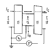
Figure 2 illustrates a re~onant tunneling
-semiconductor device functioning in a transport switching
: circuit; : :
Figure 3 illustrates a family of curves for a
resonant tunneling semiconductor device of the same type as
illustrated in Figures 1 and 2, which enable it to
'
YG986-OOZX
''~ ` :
2~ 0~4
function in a transport amplification application with
l different base voltage levels;
Figure 4 is a schematic illustration of a resonant
tunneling semiconductor device functioning in an
electro-optical lasing circuit;
Figure 5 is a schematic illustration of a resonant
tunneling semiconductor device functioning in an
electro-optical detection circuit; and
~ Figure 6 illustrates a preferred embodiment of a
contact extending to the quantum potential well of a
resonant tunneling semiconductor device constructed pursuant
to the teachings of the subject invention.
I5
Description of the Preferred Embodiments
The present invention concerns semiconductor
devices which are generally three terminal devices based on
the phenomenon of resonant tunneling. These devices are
constructed from epitaxial layers of proper materials with
suitable thickness and doping, such that the structures can
be utilized to perform a variety of ~unctions for transport
and optoelectronics under different operational conditions.
Applications for high speed switching or amplification and
for efficient light emission and detection are particularly
of interest.
.
Referring to an e~emplary embodiment in Figure 1,
3o a central region lO in which a semiconductor potential well
i5 located is formed of an opposite conductivity type to the
semiconductor layers 12 located outside of two resonant
tunneling barriers 14, such that electrons can tunnel
.
Y0986-OOZX
:
2~
- 9 -
through the barriers 14. In transport applications, the
1 central potantial well servPs as the base OI a three
terminal device, and in electro-optical applications the
central potential well serves as the light responsive or
light lasing portion. In the embodiment illustrated in
Figure 1, the device is constructed in five layers, n
Ga Al 2As, undoped Gal_x3Alx3AS, P Ga1-xl xl
G2l_x3Alx3As, n G2l_x2Alx2As, between a buffer substrate 16
and a surface layer 18, with a reachthrough contact being
provided to the p base.
' .
~ In the structure of Figure 1, the well is p-type
with composition xl (x refers the alloy composition of Al in
GaAlAs) and width dl, the outside layers are n-type with ~ `
composition x2 and width d2, and the barriers are undoped
with composition x3 and width d3. The requirements are xl~
x2<x3, and dl and d3 be of the order of 50A. The widths d2
are not critical. The n-contacts can be made in a
conventional way to the x2 layer on the surface and from the
n-substrate 16 on which the entire structure is grown, for
example by molecular beam epitaxy. The p-laver 10 can be
contacted by selective etching based on the type of
conductiuity, but is preferably constructe2 by alloying
through the surface to form a contact of the same type
semiconductor material as the quantum well, as explained in
greater detail hereinbelow with reference to Figure 6.
The use of x2 for material 12 and xl for ~aterial
10 with x2 ~xi is a necessary condition. For transport
devices, the ohmic p-contact from the surface to the central
3o Gal x1AlxlAs layer will make contacts to both the outside
n-layer (Gal x2Alx As) and the barrier intrinsic layer
(Gal x3Alx3As)(See Fig. 6). The intrinsic layer poses no
problems because it is not conductive. However the contact
YCg86-002X
2~ 0%~
--10--
to the n-layer will give rise to undesirable leakage current
l e~en for a p-n blocking contact. This problem can be
alleviated by the use of a wider gap material such as
Gal x2Alx2As with x2 ~x1. For optoelectronic devices, the
requirement, Y2~ ~1' is essential for the light to penetrate
to reach layer 10 without absorption or reabsorption in
layer 12.
The use of an alloyed contact to penetrate through
two other layers to reach the thin central well region must
be looked upon in its entirety in resonant tunneling
structures, as the art has struggled to find a solu_ion to
this problem. An etch-and-stop technique is tedious and
difficult to say the least, in particular in view of the
very thin central layer. It als~ destroys the planarity of
the structure, which is important in particular for device
arrays. Moreover, an alloying contact is different from a
dif_used contact, and diffusion has to be conducted at high
temperatures, which is alright for thick devices, but will
completel~ destroy the interface abruptness in a thin
resonant tunneling structure as in the present invention.
The essence of resonant tunneling lies in the
formation of quasi-stat~onary quantum states in the well at
specific energies~ depending on the details of the
configuration (x, d, etc.). Typically, the lowest energ~r
state is 10-lO0 meV with si~ilar spacings between the states
since more than one such state can generaIly be formed.
This is shown in Fig. l by horizontal lines for both
electron and hole states, only the former, however, are of
3o interest here. The quantum states provide an effective
channel of electron tunnelins between the barriers. At
these energies, an intensive electron wave is built inside
the well so that a small leakage ou~side will result in
Yo986-002X
~ , . -
261~02~
nearly perfect transmission. On the other hand, at other
1 energies (even with a single barrier), there is virtually no
transmission.
Referrina to Figure 2, the electrodes are
desi~nated as the emitter E, the collector C, and the base
B. In operation of the circuit of Figure 2, when a voltage
applied to the base equals a threshold voltage VT, the
device becomes conductive to provide for electrical
conduction between the emitter and the collectox. For
switching operations, we note that no appreciable current
flows initially until VB = VT, the threshold voltàge, when
the device is sharply turned on. (Fig. 2). For this
purpose, VE = O and-VC is slightly positive (O ) to provide
states ~or tunneling. Since the tunnelin~ time is much
shorter than the recombination time, IC ~ IE for nearly
unit ~ain, and the base draws little current but operates as
an effective gate.
Figure 3 illustrates a family of cur~es for a
resonant tunneling semiconductor device of the same type as
illustrated in Fi~ure 1 and 2. ~ere the resonant condition
is reached by applying a voltage Vc. The current-voltage
characteristic is governed by different base voltage levels
(designated o, 1, 2). The hi~hly nonlinear current-voltage
- 25 behavior, including a negative resistance, makes these
structures capable of functioning not only as a flexible
switching device but also as an amplifier or an oscillator.
.
For optoelectronic applications, the emitt~r and
3o collector are biased at the same value, say VE = VC = O =
ground, and VB 3VT. Figure 4 is a schematic illustration of
a resonant tunneling semiconductor device functioning in an
electro-optical emission circuit. As chown in Figure 4,
Y098~-002X
. ,. ~ ~ .
2C?~S0%~ :
-12-
electrons flow into the well where they are trapped, and an
1 intense wave is built up. Strong radiative recombination
with holes occurs, leading to light emitting and lasing
actions. The reverse of this situation makes the device an
ef~ective detector (Fig. 5). Electrons generated in the
well tunnel rapidly to the outside electrodes, where
external circuitry in the form of current meters 20 are used
for sensitive detection. The application of-a bias voltage
is optional in this case.
. For operation of these devices, the penetratior.
(or traversal) time is estimated to be very short,
tt = (m/~E)1/2-. d3 where m is the electron mass and E is
the electron energy. This is calculated to be smaller than
10 14 sec, which poses no serious limit or continuous
operation. The limiting time for switching is expectedly
the storage time or the time for the electron wave to build
up or decay. It is given by ~ /T where ~ is the frequency
the electron wave striking the barrier and T is the
transmission at resonance. Typically, it is about 10
sec. The delay (or charging) time is not significant in
comparison. An estimate from gm C gives 10 sec, where C
is the capacitance and gm = ~J/av wherel J is the curren~
change at resonance and ~v is the width in resonant enerav
(hT/2~U, h being Planck's constant). The various
oharacteristic times are much shorter than the recombination
time, which is usually in the nanosecond to sub-nanosecond
range~
.. .
~ore than one quantum level is usually present.
The operations can be tuned to each level if required. In
other cases, a flat respor.se at V~ VT may be desirable.
This can be achieved by designing the structure with close
level spacings and asymmetrical barriers.
, .
Y0986-002X ;
' ~ - , .i ;i
2al~02~
-13-
Complementary structures with n-well and p-outside ` `
1 layers are equally operable, as well as the use of multiple
wells and superlattices instead of the single well. Also,
different semiconductors can be used rather than alloys with
different compositions. Indeed, combi~ations such as InAs
ana GaSb are ideal in that their band schemes closelv
resemble those shown in Figure 1 without considering the
space-charge effect which has been ne~lected. A general
requirement is that the barrier material has the laraer
energy gap throush which the carriers tunnel, and the well
material has the smallest gap to ~ascilitate contact
formation and light absorption. `
Figure 6 illustrates a preferred embodiment of a
contact extending to the quantum potential well of a
resonant tunneling semiconductcr device pursuant to the
subject invention. One problem associated with structures
of this nature is the provision of an electrical contact
extending to the quantum well, and the present invention
provides a novel solution for this problem by forming the
contact of the same type of conductivitv semiconductor
material as the central potential well. The contact is
therefore of an opposite typ of semiconductor material to
the layers of semiconductor crystal outside the first and
second barriers, such that electrical conductivity
therebetween is prevented. The co~tact is formed by an
alloy contact which is melted to form a consistent contact
throughout, as opposed to a diffusion contact which would
cause different doping levels throughout because o' the
nature of the diffusion process. Accordingly, this approach
3o allows the contact to physically contact either-one or both ^
of the layers of opposite semiconductor material without
establishin~ an electrical current path thereto.
.; '
^.
.
2~0~:4
-14-
While several embodiments and variations of the
1 present invention for resonant tunneling semiconductor
devices are described in detail herein, it shoul~ be
apparent that the disclosure and teachings of the present
invention will suggest many alternative designs to those
skilled in the art.
.
.
.
..
.
:: .
Yoss6-oo~ ~: