Note: Descriptions are shown in the official language in which they were submitted.
2~)00~)71
1 TITLE OF THE INVENTION
Recording and Reproducing Apparatus and
Recording and Reproducing Method and Recording Medium
for the Recording and Reproducing Method-
BACKGROUN~ OF THE INVENTION
Field of the Invention
The present invention relates to a recording-
reproducing apparatus for recording by employing
10 electromagnetic wave irradiation and electric field
appiication and reproducing by detecting a tunnel
current, and a recording-reproducing method employing
the apparatus. And the present invention relates to
further a novel recording medium used suitably for the
15 recording and reproducing method.
Related Background Art
Applications of memory materials are the most
important field of electronic industries such as
computors and related apparatus, video-disks, and
20 digital audio-disks. The developement of the
materials are the subject of comprehensive studies in
recent years. Although the performances required to
the memory materials depend on the application fields
thereof, the generally required performances are as
25 below:
(1) High recording density and large recording
'\C
2(~00071
1 capacity~
(2) High response speed of recording and
reproduction,
(3) Low electric power consumption, and
(4) High productivity and low cost.
and so forth.
Heretofore, semiconductor memories and
magnetic memories based on a semiconductor or a
magnetic substance are predominantly used for memory
10 materials. Lately as a result of the progress of
laser technology, low-cost and high-density recording
media have been developed employing an optical memory
by use of an organic thin film of an organic coloring
matter, a photopolymer, etc.
On the other hand, the scanning tunnelling
microscope (hereinafter referred to as STM) has been
recently developted to enable a direct observation of
an electronic structure of surface atoms or molecules
of a conductor with a resolving power of 0.1 nm [G.
20 Binnig et al., Phys. Rev. Lett. 49 (1982) 57].
Recently, by using STM, an experiment has been
conducted in which a pulse voltage is applied between
a probe electrode and an electroconductive material to
fabricate locally the surface of the electroconductive
25 material and the change of the shape or state of the
surface is read [J. S. Foster et al., Nature 331
2~)00071
-- 3
1 (1988) 324]. Further by means of the STM, switching
characteristics and rectification characteristics of
an organic molecule have been investigated [A. Aviram
et al., Chem. Phys. Lett. 146 (1988), 490].
However, even with the highest density and the
largest recording capacity of the conventionl optical
memories practically used, the recording capacity is
at most 10 bit/cm2, which is becoming insufficient to
the image recording in modern computors and video
10 apparatuses.
The recording and reproduction by use of STM,
although the recording can be conducted with a bit
size in the order of an interatomic or intermolecule
distance (0.5 to 50 nm), is not satisfactory from the
15 viewpoint of the reproductivity and stability, and yet
its recording and erasing mechanism has not been
elucidated. Moreover, in measurement of electric
characteristics by accessing a molecule by means of
STM, the record may sometimes be affected by
20 reproducing operation (voltage application) because
recording and reproduction are made by voltage
application. Therefore STM is not satisfactory for
application to memory.
25 SUMMARY OF THE INVENTION
The object of the present invention is to
2000071
- 4 -
1 provide a recordiny-reproducing apparatus satisfactory
in reproductivity and stability of recording, and has
a large recording capacity, and also to provide a
method for recording and reproducing employing the
5 apparatus. And the object of the present invention is
to provide a novel recording medium used suitably for
the recording and reproducing method.
The above object is achieved by the present
invention described below.
According to an aspect of the present
invention, there is provided a recording-reproducing
apparatus, comprising a material, in which
intramolecular electron distribution can be changed,
by electromagnetic irradiation and electric field
15 application, a probe electrode brought close to the
material, a means for projecting an electromagnetic
wave onto the material, and a means for applying an
electric field between the material and the probe
electrode.
According to another aspect of the present
invention, there is provided a recording-reproducing
apparatus, comprising a recording, in which a material
selected from the group of compounds consisting of azo
compounds, styrene derivatives and imino compounds
25 having a quinone group and hydroquione group in the
molecule, and azo compounds, styrene derivatives and
2000071
- 5 -
1 imino compounds having two amino groups in the
molecule is deposited on an electrode; a probe
electrode brought close to the recording medium; a
means for projecting an electromagnetic wave onto the
5 recording medium; and a means for applying electric
field between the recording medium and the probe
electrode.
According to still another aspect of the
preseent invention, there is provided a recording-
10 reproducing apparatus, comprising a recording medium ,in which a charge transfer complex is deposited on an
electrode, a probe electrode brought close to the
recording medium, a means for projecting light onto
the recording medium, and a means for applying
15 electric field between the recording medium and the
probe electrode.
According to a further aspect of the present
invention, there is provided a recording method
comprising projecting an electromagnetic wave and
20 simultaneously applying electric field onto a material,
in which intramolecular electron distribution can be
changed, by electromagnetic wave projection and
electric field application to cause change in the
electron distribution in the molecule of the material
25 to write information, thereby conducting information-
recording.
Z000()71
1 According to a still further aspect of the
present invention, there is provided a recording-
reproducing method, comprising conducting information-
recording by projecting an electromagnetic wave and
5 simultaneously applying electric field onto a material,
in which intramolecular electron distribution can be
changed, by electromagnetic wave projection and
electric field application thereby causing change in
the electron distribution in the molecule of the
10 material to write information; and conducting
information readout by detecting a tunnel current at
the portion where the information is recorded.
According to a still further aspect of the
present invention, there is provided a recording-
15 reproducing-erasing method, comprising conducting
information-recording by projecting an electromagnetic
wave and simultaneously applying electric field onto a
material, in which intramolecular electron distribution
can be changed, by electromagnetic wave projection and
20 electric field application thereby causing change in
the electron distribution in the molecule of the
material to write information; conducting information
readout by detecting a tunnel current at the portion
where the information is recorded; and erasing the
25 information by projecting an electromagnetic wave and
simultaneously applying electric field onto the
2Q00071
- 7 -
1 portion where the information is recorded.
According to still further aspect of the
present invention, there is provided a recording-
reproducing-erasing method, comprising conducting
5 information-recording by projecting an electromagnetic
wave and simultaneously applying electric field onto a
material, in which intramolecular electron distribution
can be changed, by electromagnetic wave projection and
electric field application thereby causing change in
10 the electron distribution in the molecule of the
material to write information; conducting information
readout by detecting a tunnel current at the portion
where the information is recorded; and erasing the
information by introducing a vibration energy to the
15 portion where the information is recorded.
According to still further aspect of the
present invention, there is provided a recording
medium, comprising providing a material capable of
causing a proton-transfer by photoisomerization on a
20 substrate.
BRIEF DESCRIPTION OF THE DRAWINGS
Fig. 1 illustrates a block constitution of the
embodiment of a recording-reproducing apparatus of the
25 present invention.
Fig. 2 illustrates a block constitution of
2(~0007~
1 another embodiment of a recording--reproducing
apparatus of the present invention.
Fig. 3 illustrates an example of the signal in
recording operation.
Fig. 4 illustrates an example of the signal in
erasing operation.
Fig. 5 shows the principle of recording by
memory materials.
Fis. 6 shows a memory material and the
principle of erasing therewith.
DETAILED DESCRIPTION OF THE PREFERRED EMBODIMENTS
The present invention is described in detail
below.
The materials employed in the present
invention are those, in which an electron distribution
in the molecule can be changed, by irradiation of an
electromagnetic wave and application of voltage.
Embodiment of the materials includes
(1) memory materials, in which a redox pair (an
oxidation-reduction pair) within the molecule or
between the molecules is formed due to isomerization
in the molecular structure b~ electomagnetic wave
irradiation, and an electron distribution in the
25 molecule is changed due to proton transfer in the
redox pair by further electric field application, and
2000~7~
_ 9 _
1 (2) memory materials, in which an molecular
distribution in the molecule is changed, by irradiation
with electomagnetic wave and simultaneous application
of an electric voltage exceeding the threshold voltage
5 for causing memory effect.
Embodiment (1) of the memory materials
includes specifically azo compounds having a quinone
group and a hydroquinone group within the molecule,
styrene derivatives having a quinone group and a
10 hydroquinone group within the molecule, imino
compounds having a quinone group and a hydroquinone
group within the molecule, azo compounds having two
amino groups within the molecule, styrene derivatives
having two amino groups within the molecule, and imino
15 compounds having two amino groups within the molecule.
Examples of the preferred compounds are shown below:
No.1
~
O ~N
OH
~OH
200~
- 10 -
No . 2
,~
\N ~ C/R ~
R 3 1I H
C~ N
R 5 ~ R,
No. 3
\N~ ~R ~
R 3 N~ - R -
No . 4
~ ~ N R,
N~ lH
2000Q71
- 11 -
1 No.5
~ R .
O~lC
C ~OH
- R z ~OH
No.6
O q~
o~ll ~R -
N ~OH
~OH
( ' 1 5 3 ' 2 s '
isopropyl, and the positions of =0, or -OH are in the
relation of ortho, meta, or para positions.)
Compounds of Nos. 1, 2, 4 and 5 among them
are particularly preferred because of a high
20 photoisomerication efficiency.
By use of these materials, the
recording/reproducing/erasing are conducted as follows.
The electromagnetic wave irradiation onto the
material causes isomerization in the molecular
25 structure, forming a redox pair in the molecule, and
further application of voltage causes proton transfer
2Q00(~71
- iz -
1 within the redox pair, resulting in change in
intramolecular electron distribution into the recorded
state of the present invention.
Erasing is conducted by irradiation of
5 electromagnetic wave onto the recorded portion and
simultaneous application of electric field in the
reverse direction to cause reversed proton transfer.
In a non-irradiated state, application of an
electric field onto the material does not cause the
10 proton transfer and the resulting change of
intramolecular electron distribution since no redox
pair is present. Thus, in the memory material
employed here, recording and erasing can be conducted
by voltage application only under irradiation of an
15 electromagnetic wave. In reproduction, since the
material is not irradiated, no change occurs in
recorded and erased states by application of an
electric field between the memory material and the
probe for tunnel current detection.
Embodiment (2) of the memory materials
includes charge transfer complexes of a metal with an
organic electron acceptor. Specific examples are, for
example, n-octadecyltetracyanoquinodimethan copper
complex (ODTCNQ/Cu), n-dodecyltetracyanoquinodimethan
25 copper complex (DDTCNQ/Cu), n-
octadecyltetracyanoquinodimethan silver complex
2000071
- i3 -
1 (ODTCNQ/Ag), n-dodecyltetracyanoquinodimethan silver
complex ~DDTCNQ/Ag), and their derivatives.
By employing these materials, the
recording/reproduction/erasing are conducted as
5 follows.
Recording is conducted by applying to a probe
electrode a voltage exceeding a threshold voltage for
giving a memory effect corresponding to the
information while irradiating an electromagnetic wave
10 (or light); reproduction is conducted by applying a
voltage to the probe electrode, and scanning the
material with the probe electrode keeping a constant
distance between the material and the probe electrode,
and detecting the change of intensity of current
15 flowing the probe electrode; and erasing is conducted
by introducing vibration energy to the material.
Such memory material is used by depositing it
on an electrode material.
As the electrode material, any material may be
20 used which is capable of forming a film having
electroconductivity and smoothness. Examples of
suitable materials are Au/Pd, Pt, n -Si, ITO, etc.
A preferable method for depositing a memory
material onto an electrode is the Langmuir-Blodgette
25 process in view of easiness of formation of a uniform,
and defectless thin film with high regularity.
2000()71
- 14 -
1 For projecting an electromagnetic wave OlltO
the memory material, any electromagnetic wave source
may be employed which emits a light having a
wavelength of from visible to infrared retions.
5 Various light sources can be used as desired such as a
xenon lamp, a helium-neon laser, an argon laser, a
semiconductor laser, and carbon dioxide laser. The
application voltage may be varied in connection with
the light intensity.
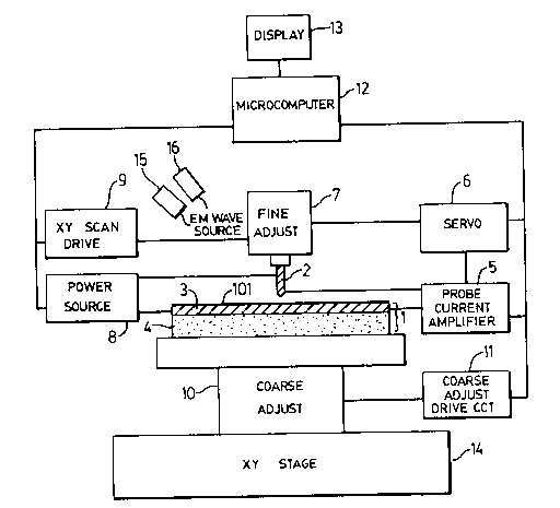
Fig. 1 illustrates a block constitution of a
recording apparatus of the present invention, where
the numeral 5 denotes a probe current amplifier; 6
denotes a servo circuit for controlling fine adjusting
mechanism 7 which employs a piezo-element to maintain
15 the probe corrent constant; and 8 denotes a power
source for applying a pulse voltage between probe
electrode _ and electrode 3 for recording/erasing.
On application of a pulse voltage, the probe
current abruptly changes, so that servo circuit 6
20 controls the HOLD circuit to be in an ON state during
the change to maintain the output voltage constant.
9 is an XY scan-driving circuit for
controlling the movement of probe electrode 2 in the
XY directions. 10 is a coarse adjusting mechanism
25 and 11 is a coarse adjusting-driving circuit, which
coarsely control the distance between probe electrode
2000071
- 15 -
1 2 and recording medium 1 so as to give a probe current
of approximately 10 A. These mechanisms are all
subjected to central control of microcomputor 12. 13
is a display device. 14 is an XY stage. 15 and 16
5 are each an electromagnetic wave source.
Examples of the mechanical performances in
movement control employing a piezo-element are shown
below.
Range of fine movement control in the Z direction:
o.1 nm to 1 nm
Range of coarse movement control in the Z
direction: lO nm to 10 mm
Range of scanning in the XY directions:
0.1 nm to 1 nm
Tolerance in measurement and control:
less than 0.1 nm
The examples below are intended to illustrate
specifically the present invention.
Example 1
Fig. 1 illustrates a recording-reproducing
apparatus of the present invention. Probe electrode 2
is made of platinum/rhodium. Probe electrode 2 is
finely controlled by a piezo-element to keep the
distance (Z) from the surface of recording layer 101
25 to maintain the current at a constant level. Fine
movement control mechanism 7 is designed to control
2000~J71
- 16
1 finely the movement of the probe electrode in the
plane (XY) direction with retention of the distance Z.
Probe electrode 2 is capable directly of recording,
reproducing and erasing information. The recording
5 medium is placed on XY stage 14 and can be moved to a
desired position.
The film of octadecyltetracyanoquinodimethan
copper complex (ODTCNQ/Cu) was formed in the following
procedure. A solution of 4 x 10 M ODTCNQ/Cu in
10 acetonitrile (ACN~ was prepared. The solution was
spread on pure water at 20C, and the surface pressure
was raised to 20 mN/m to form a monomolecular film on
the surface of water. A glass substrate having a
vapor-deposited gold/palladium (Au/Pd) film of 300 A
15 thick which had been previously immersed in the water
phase was slowly pulled up at a rate of 5 mm/min in
the direction crossing the water surface with the
surface pressure maintained constant to form a
monomolecular film of ODTCNQ/Cu on the glass substrate
20 having vapor-deposited Au/Pd. This was employed as
recording medium 1.
The experiment on recording-reproducing-
erasing was conducted by employing recording medium 1
having a monolayer LB film of the ODTCNQ/Cu. Firstly,
25 recording medium 1 was placed on XY stage 14, and
probe electrode 2 was fixed at a visually determined
200(~()7~
- 17 -
1 position. The distance Z between probe electrode 2
and the surface of recording layer 101 was adjusted by
applying the voltage of 3 V between Au/Pd electrode 3
and the probe and by monitoring the current. On
5 application of voltage of +300 mV to probe electrode
2, the current was found to be not more than 1 pA.
After stopping an application of the voltage,
the recording was conducted by irradiating a light to
recording medium 1 with xenon lamp 15 and by applying
10 again a voltage of +5 V to probe electrode 2. The
recording medium was found to have transferred to an
ON state in which the electricity flowed well.
The light irradiation and the voltage
application were stopped, and then at the same
15 position, a voltage of +300 mV was applied to probe
electrode 2 to reproduce the record. A current of 5
nA was found to flow there, which shows the retention
of the ON state, namely the retention of the record.
After stopping an application of a voltage
20 argon laser 16 was projected onto the recorded portion
and vibration energy was given thereto. The vibration
energy shall mean here an electromagnetic wave having
about one figure smaller energy amount than that of an
electromagnetic wave used for recording. Thereafter
25 at the same position, a voltage of +300 mV was applied
again to probe electrode 2 to reproduce the record. A
2000()71
- 18 -
1 current of not more than 1 pA was found to flow, which
shows the transition to an OFF state, namely erasure
of the record.
Example 2
The recording-reproducing apparatus
illustrated in Fig. 1 was employed in the same manner
as in Example 1.
The film of dodecyltetracyanoquinodimethan
copper complex (DDTCNQ/Cu) was formed in the following
10 procedure. A solution of 4 x 10 M DDTCNQ/Cu in
acetonitrile (ACN) was prepared. The solution was
spread on pure water at 20C, and the surface pressure
was raised to 20 mN/m to form a monomolecular film on
the surface of water. A glass substrate having a
15 vapor-deposited gold/palladium (Au/Pd) film of 300 A
thick which had been previously immersed in the water
phase was slowly pulled up at a rate of 5 mm/min in
the direction crossing the water surface with the
surface pressure maintained constant to form a
20 monomolecular film of DDTCNQ/Cu on the glass substrate
having vapor-deposited Au/Pd. This was employed as
recording medium 1.
The experiment on recording-reproducing-
erasing was conducted by employing recording medium 1
25 having a monolayer LB film of the DDTCNQ/Cu. Firstly,
recording medium 1 was placed on XY stage 14, and
2000C)71
-- 19 --
1 probe electrode 2 was fixed at a visually determined
position. The distance Z between probe electrode 2
and the surface of recording layer 101 wa~ adjusted by
applying the voltage of 3 V between Au/Pd electrode 3
5 and the probe and by monitoring the current. On
application of voltage of +300 mV to probe electrode
2, the current was found to be not more than 1 pA.
After stopping an application of the voltage,
the recording was conducted by irradiating a light to
10 recording medium 1 with xenon lamp 15 and by applying
again a voltage of +5 V to probe electrode 2. The
recording medium was found to have transferred to an
ON state in which the electricity flows well.
The light irradiation and the voltage
15 application were stopped, and then at the same
position, a voltage of +300 mV was applied to probe
electrode 2 to reproduce the record. A current of 5
nA was found to flow, which shows the retention of the
ON state, namely the retention of the record.
After stopping an application of the voltage,
argon laser 16 was projected onto the recorded portion
and vibration energy was given thereto. Thereafter at
the same position, a voltage of +300 mV was applied
again to probe electrode 2 to reproduce the
25 record. A current of not more than 1 pA was found to
flow, which shows the transition to an OFF state,
Z(~00(~71~
- 20 -
namely erasure of the record.
~xample 3
The recording-reproducing apparatus
illustrated in Fig. 1 was employed in the same manner
5 as in Example 1.
The film of octadecyltetracyanoquinodimethan
silver complex (ODTCNQ/Ag) was formed in the following
procedure. A solution of 4 x 10 M ODTCNQ/Ag in
acetonitrile (ACN) was prepared. The solution was
10 spread on pure water at 20C, and the surface pressure
was raised to 15 mN/m to form a monomolecular film on
the surface of water. A glass substrate having a
vapor-deposited gold/palladium (Au/Pd) film of 300 A
thick which had been previously immersed in the water
15 phase was slowly pulled up at a rate of 5 mm/min in
the direction crossing the water surface with the
surface pressure maintained constant to form a
monomolecular film of ODTCNQ/Ag on the glass substrate
having vapor-deposited Au/Pd. This was employed as
20 recording medium 1.
The experiment on recording-reproducing-
erasing was conducted by employing recording medium 1
having a monolayer LB film of the ODTCNQ/Ag. Firstly,
recording medium 1 was placed on XY stage 14, and
25 probe electrode 2 was fixed at a visually determined
position. The distance Z between probe electrode 2
2000071
- 21 -
1 and the surface of recording layer 101 was adjusted by
applying the voltage of 3 V between Au/Pd electrode 3
and the probe and by monitoring the current. On
application of voltage of +300 mV to the probe
5 electrode 2, the current was found to be not more than
1 pA.
After stopping an application of the voltage,
the recording was conducted by irradiating a light to
recording medium 1 with a helium-neon laser in place of xenon
10 lamp 15 and applying again a voltage of +3 V to probe
electrode 2. The recording medium was found to have
transferred to an ON state in which the electricity
flowed well.
The light irradiation and the voltage
15 application were stopped, and then at the same
position, a voltage of +300 mV was applied to the
probe electrode 2 to reproduce the record. A current
of 5 nA was found to flow, which shows the retention
of the ON state, namely the retention of the record.
After stopping an application of the voltage,
a carbon dioxide laser in place of argon laser 16 was
projected onto the recorded portion and vibration
energy was given thereto. Thereafter at the same
position, a voltage of +300 mV was applied again to
25 probe electrode 2 to reproduce the record. A current
of not more than 1 pA was found to flow, which shows
2000071
1 the transition to OFF state, namely erasure of the
record.
Example 4
The recording-reproducing apparatus
5 illustrated in Fig. 1 was employed in the same manner
as in Example 1.
The film of octadecyltetracyanoquinodimethan
silver complex (ODTCNQ/Ag) was formed in the following
procedure. A solution of 4 x 10 M ODTCNQ/Ag in
10 acetonitrile (ACN) was prepared. The solution was
spread on pure water at 20C, and the surface pressure
was raised to 15 mN/m to form a monomolecular film on
the surface of water. An n -Si substrate which had
been previously immersed in the water phase was slowly
15 pulled up at a rate of 5 mm/min in the direction
crossing the water surface with the surface pressure
maintained constant to form a monomolecular film of
ODTCNQ/Ag on the n -Si substrate, which was employed
as recording medium 1.
The experiment on recording-reproducing-
erasing was conducted by employing recording medium 1
having a monolayer LB film of the ODTCNQ/Ag. Firstly,
recording medium 1 was placed on XY stage 14, and
probe electrode 2 was fixed at a visually determined
25 position. The distance Z between probe electrode 2
and the surface of recording layer 101 was adjusted by
2000071
- 23 -
1 applying the voltage of 3 V between electrode (n -Si)
3 and the probe and by monitoring the current. On
application of voltage of +300 mV to probe electrode
2, the current was found to be not more than 1 pA.
After stopping an application of the voltage,
the recording was conducted by irradiating a light to
recording medium 1 with helium-neon laser 15 and by
applying again a voltage of +3 V to probe electrode 2.
The recording medium was found to have transferred to
10 an ON state in which the electricity flowed well.
The light irradiation and the voltage
application were stopped, and then at the same
position, a voltage of +300 mV was applied to probe
electrode 2 to reproduce the record. A current of 5
15 nA was found to flow, which shows the retention of the
ON state, namely the retention of the record.
After stopping an application of the voltage,
carbon dioxide laser 16 was projected onto the
recorded portion and vibration energy was given
20 thereto. Thereafter at the same position, a voltage
of +300 mV was applied again to probe electrode 2 to
reproduce the record. A current of not more than 1 pA
was found to flow, which shows the transition to OFF
state, namely erasure of the record.
25 Example 5
Fig. 2 illustrates an example of another
2000071
- 24 -
1 embodiment of the present invention. In the Fig.,
memory material 103 ~described later) i5 adhered by
the Langmuir-Blodgette process or other method onto
electroconductive transparent electrode 102 such as
5 IT0 (indium-tin oxide) provided on glass plate 101.
Further probe 104 is brought to proximity of
approximately sub-nanometer to the desired position of
the memory material by means of a probe-position-
controlling means. Probe 104 is made of an
10 electrolytically polished tungsten wire, a
mechanically cut platinum wire, or the like having a
sharp tip (a radius of curvature of less than 1 ,um)
and is electroconductive. Probe-position-controlling
means 105 comprises such as a PTZ element and serves
15 to move probe 104 to a desired position within a plane
and the normal line direction in the memory area.
Writing/erasing is conducted in the following
manner. Firstly, electromagnetic wave 108 is
projected onto memory material 103 in the memory
20 region through the glass substrate 101 and the
transparent electrode by operating electromagnetic
wave source 107 with lens 109 in accordance with the
signal from writing/erasing signal generator 106.
Simultaneously the signal from
25 writing/erasing singal generator 106 is sent to
transparent electrode 102 to apply the electric field
2()00071
- 25 -
1 formed between transparent electrode 102 and probe 104
to the desired position of memory material 103, thus
writing or erasing being conducted.
Examples of the signals in writing are shown
5 in Fig. 3A to Fig. 3C. Fig. 3A shows a signal given
to probe-position-controlling means 105, by which
probe 104 accesses the desired position in the memory
region. Fig. 3B shows an electromagnetic-wave-source-
operating signal. Fig. 3C shows a writing signal
10 given to the memory material. The writing is
conducted at a memory position where the two signals
are given simultaneously (namely region M in Fig.3).
Examples of signals in erasing are shown in
- Fig. 4A to Fig. 4C, which illustrate erasing in the
15 region where the writing has been conducted in the
process shown in Fig. 3. Fig. 4A and Fig. 4B are the
same as Fig. 3A and Fig. 3B, and Fig. 4C shows an
erasing signal given to the memory material. The
erasing is conducted at a memory position where the
20 two kinds of signals are given simultaneously (namely
region E in Fig. 4).
Readout is conducted in the following manner.
A bias voltage is applied by bias source 110 onto the
memory material on transparent electrode 102, and
25 tunnel current 111 flowing between memory material 103
and probe 104 which is in the proximity of sub-
2000071
- 26 -
1 nanometer to memory material 103 is detected by means
of current detecting circuit 112. The tunnel current
intensity at a written portion (being in an ON state)
is different from the intensity at a non-written
5 portion or an erased portion (being in an OFF state)
on memory material 103 because the electron
distribution state on the surface and the inside of
the memory material is different between the two
state. This difference of the tunnel current
10 intensity is treated with readout treating circuit 113
to provide a readout signal (ON-OFF signals).
~ xamples of signals in readout operation are
shown in Fig. 3D and Fig. 4D. Fig. 3D shows the
tunnel current signal detected, after writing is
lS conducted as described referring to Fig. 3A to Fig.
3C, by scanning again the same region. In this
example, the tunnel current increases at the portions
corresponding to the written portions. Fig. 4D shows
the tunnel current signal detected, after erasing is
20 conducted as described by referring to Fig. 4A to Fig.
4C, by sc,anning again the same region.
The memory material employed in the present
invention and the principle of writing/erasing therein
are described below. As an example of the memory
25 material, an azo compound is taken which has the
structure shown in Fig. 5A (in which the positions of
2000~1
- 27 -
1 the quinone groups, and the hydroquinone groups
include ortho, meta, and para positions). Irradiation to
the compound with light of wavelength of 400 nm causes
photoisomerization from the trans configuration to the
5 cis configuration at the azo group in the molecule to
give the structure shown in Fig. SB. With the
irradiation of the light maintained, the application
of an electric field between transparent electrode
102 and probe 104 in the direction as shown in the
10 figure causes proton (H ) transfer between the quinone
group and the hydroquinone group, which are in a
hydrogen-bonded state, giving the structure shown in
Fig. 5C. On stopping the light irradiation, a
photoisomerization occurs again from the cis
15 configuration to the trans configuration to give the
structure shown in Fig. 5D. This structure
corresponds to the written state which is different
from the structure of the initial state shown in Fig.
5A in the intramolecular electron distribution and is
20 caused by the proton transfer between the hydroquinone
group and the quinone group. As the result, the shape
of the tunnel barrier between transparent electrode
102 and probe 104 changes corresponding to the
structure as shown in Fig. 5A (the initial state) and
25 the structure as shown in Fig. 5D (the written state),
thus giving the change of the tunnel current intensity
2aoc~7l
- 28 -
1 flowing under the application of the bias voltage
between transparent electrode 102 and probe 104. The
detection of this change enables the discrimination of
the states of the molecules (the initial state and the
5 written state) at the position, to which probe 104 is
in access. An example of the detected tunnel current
signals are shown in Fig. 3D, corresponding to the
instance of Fig. 3A to Fig. 3C in which the tunnel
current rises at the portion in the written state in
10 comparison with the initial state.
The erasing of the written state of the memory
material shown in Fig. 5 is explained in reference to
Fig. 6. Irradiation with light of wavelength of 400
nm onto the compound having the structure shown in
15 Fig. 6A in a written state causes photoisomerization
of the compound from the trans configuration to the
cis configuration at the azo group in the molecule to
give the structure shown in Fig. 6B. With the light
irradiation maintained, the application of an electric
20 field between transparent electrode 102 and probe 104
in the direction shown in Fig. 6C (in the direction
reverse to that shown in Fig. 5C) causes proton (H )
transfer between the quinone group and the
hydroquinone group which are in a hydrogen-bonded
25 state, giving the structure shown in Fig. 6C. On
stopping the light irradiation, the photoisomerization
- .
2(~00071
1 occurs again from the cis configuration of the trans
configuration to give the structure shown in Fig. 6C.
This structure corresponds to an erased state which is
the same as the initial state shown in Fig. 5A. The
5 erasing of the written state is conducted in such a
manner. An example of the detected tunnel current is
shown in Fig. 4D corresponding to Fig. 4A to Fig. 4C.
In the position where once writing was conducted and
then erasing has been conducted, the tunnel current
10 falls to the same value as that at the initial state.
The experiments of recording-reproducing-
erasing were repeatedly conducted with the memory
material shown in Fig. 5 and Fig. 6 by employing the
apparatus having the constitution as shown in Fig. 2
15 in the same manner above. The result showed that
recording/erasing could be made at least approximately
100 times of repetition without deterioration of the
memory material and the reproduction without causing
the change of the recording-erasing state.
The memory materials employed in the present
invention are those capable of undergoing
photoisomerization between a trans configuration and a
cis configuration (or between a syn configuration and
an anti-syn configuration) on light irradiation. Such
25 materials include those having a carbon-carbon double
bond or an imino group in addition to the material
2000071
- 30 -
1 employed in the above examples having an azo group.
The redox pair undergoing proton transfer on
application of an electric field includes a hydrogen
bonding system of amino group-amino group in addition
to the hydrogen bonding system of quinone group-
hydroquinone group employed in the above examples.
As described above, the recording-reproducing
apparatus of the present invention which is based on
the principle of STM can conduct recording and erasing
10 by electromagnetic wave irradiation and electric field
application on a memory material, and conduct
reproduction by tunnel current detection, so that it
enables a large capacity of recording and reproducing
without change of record at reproduction with
15 reproducibility and stability. With a bit size of 10
nm for the recording, a large capacity of a recording-
reproducing apparatus of as large as 1012 bit/cm2 is
achievable.
Further, the present invention has the
20 advantages as follows: The formation of a
monomolecular film in the present invention according
to an LB process can give a film having an excellent
order of the molecules and a high density, which is
suitable for super-high-density recording media. An
25 erroneous writing is prevented at the time of
2~ ()071
- 31 -
1 reproduction because recording is conducted under
irradiation of light. The storage stabilty is
excellent because erasing of a record requires a
vibration energy to be given.
s