Note: Descriptions are shown in the official language in which they were submitted.
2~10~
The present invention relates to a superconductor for
magnetic field shield which shields magnetic fields using
superconductive materials.
As a magnetic field shield utilizing superconductivity, the
first class superconductor or the second class superconductor
has been used depending on the int~nsity of a magnetic field.
The magnetic field shield using the first class
superconductor utilizes perfect diamagnetism (Meissner
effect), a characteristic of superconductivity. This
magnetic field shield cannot shield intense magnetic fields
since its critical magnetic flux density is low. The
magnetic field using the second class superconductor utilizes
the above-mentione`d perfect diamagnetism and the diamagnetism
obtained by a mixture of the superconduction state and the
normal conduction
~;' .
- , .
20001~4
state. The critical magnetic field is separated
into the upper and lower critical magnetic ~ields.
Since the intensity of the upper critical magnetic
field is extremely high, the magnetic field shield
using the second class superconductor can be used to
shield intense magnetic fields.
Superconductive shielding and electromagnetic
shielding are used to shield magnetic fields using
superconductors. Superconductive shielding uses the
perfect diamagnetism (a characteristic of
superconductivity) and the diamagnetism obtained by
the above-mentioned mixture condition. In the case
of electromagnetic shielding, what is called
interlinkage magnetic flux unchangeability principle
is used to generate magnetic fluxes, the direction
of which is opposite to that of the magnetic fluxes
interlinking in a closed circuit obtained by
connecting conductors one after another.
As a magnetic field shielding application example of
the above-mentinned second class superconductor, a
superconductive sheet or tape wound around a
cylindrical core material is used. An example of
this type is disclosed as the Japanese Provisional
,
.
,
:, ' ~ '~ '' ' ' " ;' `
Z0001~:P4
Patent Publication No. 56-40289. This magnetic
field shield is disposed in an intense magnetic
field to shield the interna:L space of the core
material against external magnetic fields, or used
to prevent the magnetic field of a magnet disposed
in the core material from leaking outside.
The U.S.A. Letters Patent No. 3,281,738 discloses a
superconductive solenoid. In this superconductive
solenoid, discs on which superconductive rings are
formed coaxially and discs made of a material
superior in thermal and electrical conductivity are
laminated alternately to form a cylinder. This
cylinder is intended to be used as a magnet by
taking magnetic fluxes inside. It can also be used
as a magnetic field shield since it contains
superconductors between the internal and external
spaces.
The shield composed of a cylindrical core material
on which the above-mentioned superconductive sheet
or tape is wound is used to electromagnetically
shield the internal and external sides of the core
material via the junction at the ends of the
superconductive sheet or the junctions at the
'
, :, `
- ~ , .
~ .
Z~lOlC~9,
fringes of the superconductive tape. Therefore, the
junction condition greatly affects the magnetic
field shielding effect. The above-mentioned
Japanese Patent Provisional Publication discloses a
method wherein a superconductive sheet is wound
around a core material and dipped in a melted metal
(with a low melting point) to join the fringes of
the superconductive tape. In this case, however,
the melted metal is not fully distributed and the
thickness of the metal layer is not uniform. As a
result, the shield has a low shielding effect to a
magnetic fieId parallel to the axis of the core
material and the effect reduces secularly. When the
shielding effect on the surface area of the shield
to a magnetic field is examined, no electrical
interlinkage condition by the superconductive tape
is not formed since the low melting point metal
discontinues at some portions. The interlinkage
magnetic flux unchangeability principle cannot
function sufficiently. In addition, differences in
electrical resistance are caused due to differences
in thickness of the low melting point metal. At a
thick portion, Joule heat generates and the
~. ' ' ,
. . . , . ~ .
.- - ~ - . . .
20001~4
electrical interlinkage condition is apt to be lost
secularly.
As another example, a net tape including a
superconductive wire material is wound on a
cylindrical core material and joined using Wood's
metal or solder. This shield has numerous`junctions
and its magnetic`field shielding effect reduces
secularly due to the electrical resistance generated
at the junctions.
When the superconductive solenoid of the above-
mentloned U.S.A. Patent is used as a magnetic field
shield, it is estimated to be superior to the
above-mentioned shield in the shielding stability
and secular shielding characteristics. The
superconductive disc of the solenoid is made by
coating numerous coaxial rings (ring width: 0~02 to
0~16 cm) of a superconductive material (NbTi for
example) on at least one slde of a metal substrate~
The ring width is set to 0~16 cm or less. If it
exceeds 0.16 cm, eddy current generates and the
intensity of the magnetic field to be trapped is
reduced. The multiple coaxial rings formed on the
disc ensure the total magnetic field trap amount for
~` ~ 5
. .: . , ~ . . . .,:
' '- ~ , :, ,
;~' ' ` ' ' `
:,~ ' ' '
20~0104
a single superconductive disc. When the disc is examined in
the viewpoint of magnetic field shielding, the narrow width
of the superconductive material reduces the magnetic field
shielding effect. Therefore, a large structure is required
to obtain even a small shielding space. Accordingly, the
above-mentioned superconductive solenoid is hardly applicable
to a magnetic field shield. The superconductive discs and
the above-mentioned metal discs are alternately laminated.
Because grooves are present between the superconductive
rings, magnetic fluxes enter via the metal discs and grooves
when the thickness of the metal discs is increased. To
prevent this problem, the thickness of the metal discs should
be as small as possible. However, when thin discs are used
in a magnetic field shield, the proper shielding space of a
shield structure cannot be adjusted easily depending on the
size of the object to be shielded.
After carefully examining the secular reduction of the
magnetic field shield effect due to the presence of
junctions, effective shielding, and formation of effective
spaces and machinability of effective shielding spaces in the
above-mentioned magnetic field shield, the inventors of the
present invention completed a superconductor for magnetic
field shield extremely superior and stable in magnetic field
shielding effect without causing any secular reduction of the
effect and capable of forming a large shielding space using a
:.
- 20~01~3~
minimum amount of materials and disclose the invention
herein. The applicants of the present invention have already
disclosed superconductors for magnetic field shield featuring
superior magnetic field shielding functions in the Japanese
Patent Applications No. 60-024254, No. 62-68499 and No. 63-
200795. Therefore the present invention provides an
extremely effective shielding space using these
superconductors for magnetic field shield.
The invention will be further described by reference to the
accompanying drawings, in which:
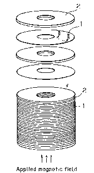
Fig. 1 is a partially exploded perspective view illustrating
a superconductor for magnetic field shield of the present
invention;
Fig. 2 is an enlarged sectional view taken on line II-II of
Fig. l;
Figs. 3 to 6 are views of other embodiments of the present
invention similar to Fig. 2;
Figs. 7 and 8 are perspective views of another embodiment of
the present invention; and
~ - .
: ` :
: ' '
~', ' .
~. .
: . - ,
:, . . , . ,, , . ~ .
- 20~19~
Figs. g and 10 are magnetic field shielding characteristic
curve graphs of the embodiments of the magnetic field shield
of the present invention.
The structure of the present invention is explained below
referring to the attached drawings. The superconductor for
magnetic field shield of the present invention comprises
closed-ring disc-shaped superconductive magnetic field
shielding members 1 and disc-shaped spacing members 2 having
the same shape as that of the magnetic field shielding member
1 and alternately laminated with the shielding members 1, the
superconductor for magnetic field shield being characterized
in that the shielding member 1 is comprised of a
superconductive layer 3 having a thickness of 500 ~m or less
and closely laminated with metal layers 4 having superior
thermal and electrical conductivity and that the ring width
of the superconductive layer 3 is 2 mm or more.
.. ~, : ' . ' :
:-. .. , . :
: . ~ - .
: . . . . . .
.: .
: , . :
2000la4
The superconductor for the shielding member 1
includes one to several tens of superconductive
layers. When only one superconductive layer 3 is
used, it is closely laminated with two metal layers -
4 on both sides of the superconductive layer 3 (as
shown in Fig. 2). When two or more superconductlve
layers 3 are used, it is necessary that the metal
layers 4 are closely inserted between at least two
superconductive layers 3 (as shown in Fig. 3). The
close mutual lamination of the superconductive
layers 3 and the metal layers 4 are usually made by
sputtering or electrodeposition of metal on a
superconductive sheet. When a plurality of the
electrodeposited composites are laminated, they are
dipped in a low-point melting metal bath and
compressed.
The superconductive layer 3 is made of niobium,
niobium compound, niobium alloy, vanadium compound
or vanadium alloy. More specifically, Nb, Nb-Ti
alloy, Nb~Zr alloy, NbN, NbC, NbN-TiN (mixed crystal
proposed in the Japanese Patent Application No. 63-
200795), Nb3Sn, Nb3Al, Nb3Ga, Nb3Ge, Nb3(AlGe) or
V3Ga is used. In addition, ceramic~based
. .
' . ` ' '
~'` ` , ' ' ' '
20001~4
superconductive material (for example, Ba-Y-Cu-O
based compound, La-Sr-Cu-O based compound,
Bi-Sr-Ca-Cu-O based compound and Tl-Ba-Ca-Cu-O based
compound) or Chevrel superconductive material (for
example, PbMo6S6) is also used.
The thickness of the superconductive layer 3 is set
to 500 ,um or less so that the cooling and
stabilization effect by the metal layer 4 is
obtained effectively. According to the relationship
between the thickness of the superconductive layer
and the magnetic field shielding effect disclosed in
the Japanese Patent Application No. 60-024254
(Japanese Patent Provisional Publication No. 61-
183979), the magnetic field shielding effect
abruptly increases from the vicinity of the origin
of the graph indicating the relationship and -then
gradually increases as the thickness of the
superconductive layer increases. If the thickness
of the superconductive layer is less than that
corresponds to the turning point where the above-
mentioned abrupt increase of the shielding effect
shifts to the gradual increase, the magnetic field
shielding effect by the multiple layers of the
~- 10
.
. . ~
,: '` ' . `
,' .
- ,
~; ~ '` ` ' ' ' " ' ,
: . .
`:`
~ooola4
superconductive layers increases synergetically.
This is highly desirable to increase the shielding
effect.
The ring width of the superconductive layer 3 is set
to 2 mm or more to generate eddy current on the ring
of the superconductive layer 3 so that the perfect
diamagnetism and the diamagnetism are caused by the
eddy current. In other words, if the ring width of
the layer 3 is below 2 mm, the above-mentioned eddy
current is not generated sufficiently and the
magnetic field shielding effect due to the perfect
diamagnetism and the diamagnetism are apt to reduce.
It is also difficult to produce such superconductive
layers. There is no upper limit in the width of the
ring. The greater the width, the larger the
shielding current capable of flowing in the
superconductive layer 3 and the higher the shielding
effect.
When the superconductive layer 3 is primarily
comprised of a mixed crystal body of niobium nitride
and titanium nitride [NbNx TiNl_x (0.1 < x < 1)], a
Nb-Ti alloy layer 5 should be sandwiched between the
metal layer 4 and the superconductive layer 3 (as
11 ".
.
Z000~4
shown in Fig. 4), since NbN TiN has no affinity with
the metal layer 4. The Nb-Ti alloy layer 5 which
has ~ood affinity with the layers 3 and 4 are
sandwiched between the layers to ensure firm fixture
of the layer~. Since the metal layer 4 functions to
cool the superconductive layer 3, it must be closely
laminated with the superconductive layer 3 and
should be made of a metal superior in thermal and
electrical conductivity, such as copper, aluminum,
nickel, stainless steel, titanium, niobium or
niobium-titanium alloy.
With the superconductive magnetic field shielding
member 1, the superconductive layer 3 must be
closely laminated with the metal layer 4. When two
or more superconductive layers 3 are used, it is
possible to include a dielectric layer 6 whic~ is
superior in thermal conductivity and made of
ceramic, such as aluminum nitride, cubic boron
nitride, silicon carbide or silicon nitride, or
diamond in the layers (as shown in Fig. 5). By
including the dielectric layer 6, the
superconductive layer 3 lS electrically insul~ted
and the stabilization effect is further enhanced.
12
, . . .................. .. .
-:: :,
:
20001~
As a result, the magnetic field shielding effect by
lamination is further magnified. The dielectric
layer 6 is thus desirably used.
The magnetic field shielding member 1, a closed-ring
disc, can have a plurality of small holes 7 passing
through the disc in the direction of the thickness
(as shown in Fig. 6). These small holes 7 feature
electromagnetic shielding as disclosed in the
Japanese Patent Applications No. 62-068499 and No.
63-200795. The area of the small holes 7 should be
3 cm2 or less and the open area rate of the entire
area to the holes 7 should be 90% or less. If the
area exceeds 3 cm2 and the open area rate exceeds
90%, the strength of the laminated layers is
insufficient when subjected to stress during
handling in an intense magnetic field, and the area
of the superconductive layer 3 becomes smaller.
This reduces shielding current (which flows to
generate.a magnetic field used to cancel the
environmental magnetic field) required to shield an
intense magnetic field. In addition, if the area of
the small hole exceeds 3 cm2, the magnetic field for
shielding inside each small hole has an inclination,
13
:. ;
. . '
. - : ..
-
" ~ ` . :-,.,
2000~LQ4
preventing complete shielding at each small hole.
On the other hand, if the area of the small hole is
too small, clogging is apt to occur during
- sputtering.
The spacing member 2 is used to provide a proper
distance in the lamination of the superconductive
magnetic field shielding members 1, and composed of
aluminum, copper or synthetic resin, such as epoxy
resin. The shielding members 1 are laminated with
the spacing members 2 using an external frame made
of a non-magnetic material for example. When a
plurality of layers are laminated, the shielding
members 1 are alternately laminated with the spacing
members 2, or a plurality of units comprising a
plurality of the shielding members 1 are alternately
laminated with the spacing members 2.
Moreover, as an additional embodiment of the present
invention, it is possible to coaxially insert a
metallic cylinder 8, the exterior of which is coated
with a superconductive sheet or film 81, into the
central open space of the laminated superconductive
shielding members 1 and the spacing members 2 (as
shown 1n Fig. 7). It i9 also possible to insert the
14
- ~ :
~OOOlQ4
laminated superconductive shielding members l and
the spacing members 2 into the metallic cylinder 8
(as shown in Fig. 8). When only the above-mentioned
lamination structure is used, it has a relatively
low shielding effect to magnetic fields
perpendicular to the axis of the structure, although
it has a superior shielding effect to magnetic
fields parallel to the axis. The additional
embodiment is used to compensate for this deficit.
The above-mentioned superconductive materials can be
used for the superconductive sheet or film 81. When
joining the superconductive materials with the
metallic cylinder 8 and when joining the
superconductive materials with each other, a
commercially available adhesive can be used as well
as a pressure joining method using a low melting
point metal. When winding a wide superconductive
sheet or tape, it is not absolutely necessary to
join the leading end with the trailing end of the
sheet or tape, because the lamination structure can
- fully shield magnetic fields generated in parallel
to the axis. Because of the same reason, both ends
of the cylinder 8 can be opened.
- ~ , , .
:: .
..
-
' ~ .. , ` ~`
2(~)01Q4
The functions of the superconductor for magnetic
field shield of the present invention are detailed
below. When the superconductor for magnetic field
shield structure is disposed in a magnetic field
which is parallel to the axis of the structure,
shielding current is generated by the magnetic field
which is parallel to the axis. This shielding
current flows in the shielding member 1 and prevents
the magnetic field from passing through. At this
time, the superconductive layer 3 in the shielding
member 1 is a complete closed loop and has no
junction. Therefore, the shielding effect is
maintained secularly.
The superconductive layer 3 of the shielding member
1 has the Meissner effect (perfect diamagnetism) and
the diamagnetism in the mixed condition of the
superconduction and normal conduction. In other
words, the magnetic field is repulsed by these
inherent characteristics of the superconductive
member and is prevented from passing. When a
plurality of the shielding members 1 are laminated,
the above-mentioned two shielding effects are
combined and the magnetic field is shut off by the
.. .. .
, ~'` ' ' ~ '
:,,
200~la4
shielding members 1 one after another. As a result,
the magnetic field is completely prevented from
passing into the space inside the object to be
shielded.
As described above, the shield of the present
invention uses a combination of superconductive
shielding and electromagnetic shielding. The
superconductive layer 3, a major element of magnetic
field shielding, is closely laminated with the metal
layer 4 which is superior in thermal and electrical
conductivity, and the shielding effect is stabilized
by the cooling effect of the metal layer 4.
Therefore, the magnetic field shielding effect is
enhanced by increasing the number of the shielding
members 1 and/or the superconductive layers 3 and by
increasing the ring width of the superconductive
layer 3. Since the shielding members 1 are
laminated with the spacing members 2, the magnetic
field shielding effect can be adjusted as desired by
selecting the thickness and the number of the
spacing members 2. Furthermore, the size of the
internal space in the shield can also be adjusted
depending on the size of the object or magnet to be
.
2aoo~
shielded.
When the small holes 7 passing through the magnetic
field shielding member 1 and the spacing members 2
are provided in the direction of the thickness,
electromagnetic shielding is produced at the small
hole sections and superconductive shielding is
produced at the other sections using the complete
diamagnetism and the above-mentioned mixed-condition
diamagnetism. In other words, the electromagnetic
shielding effect by the small holes 7 is added to
the above-mentioned superconductive shielding
effect, further increasing the magnetic field
shielding effect.
When the shield comprising the metallic cylinder 8
externally coated with the superconductive shèet or
film 81 and inserted in the central space of the
laminated structure or the shield comprising the
laminated structure inserted into the metallic
cylinder 8 is placed where it is subjected to a
magnetic field perpendicular to the axis of the
structure, the superconductive sheet or film 81
coated over the metallic cylinder 8 shuts off the
perpendicular magnetic field. This effect is
18
..;
~ `
ZOOO~Q4
combined with the above-mentioned magnetic field
shielding effect to produce three-dimensional
magnetic Eield shielding.
(EMBODIMENTS)
[1] Using a sputtsring unit equipped with a take-up
mechanism, superconductive layers made of NbTi were
alternately laminated with metal layers made of Cu
on an aluminum substrate measuring 15 ,um in
thickness and several meters in length. As such
laminated structures, the following types were
prepared: a single layer type including a 2 ~m thick
NbTi layer and another single layer type including a
4 ,um thick NbTi layer (the NbTi layer was sandwiched
between the aluminum substrate and the Cu layer),
two-layer types including two 2 ,um thick layers tthe
NbTi layer, Cu layer and NbTi layer were laminated
on the aluminum substrate in that order) and a
three-layer type including three layers (the NbTi
layer, Cu layer, NbTi layer, Cu layer and NbTi layer
were laminated on the aluminum substrate in that
order). These laminations were cut into discs
measuring 35 mm in diameter and provided with a 10
mm diame~er hole at the center. These were used as
19
.~
'
j~ .
20(~01Q4
the superconductive shielding members (embodiments 1
to 7) of the present invention. The aluminum
substrate was used as the metal layer of the present
invention.
[II] The NbTi and Cu layers were laminated on the
aluminum substrate inside a sputtering unit similar
to that described above. On the lamination, nitride
alumina ceramic was formed by the reactive
sputtering method in the atmosphere of argon and
nitrogen gases using aluminum as a target. On the
aluminum nitride layer, the Cu and NbTi layers wère
formed in the same manner as described above. This
was used as another superconductive shielding member
(embodiment 8).
~III] Using the sputtering method similar to that
described above, small holes measuring 50 ~m in
diameter were provided in a Cu substrate at an open
area rate of 20%. On the Cu substrate, NbTi
superconductive layers and Cu metal layers were
alternately laminated. In this case, five 4 ,um NbTi
layers were used. Each Cu layer was sandwiched
between two NbTi layers. A Cu layer was placed on
the top. This lamination was cut into a closed-ring
2000~04
disc as described above to form another
superconductive shielding member (embodiment 9).
The Cu substrate was used as the metal layer of the
present invention.
[IV] The NbTi superconductive layer was rolled into
a specified thickness. As a metal layer, Cu was
coated over the entire surface of the NbTi layer by
electrodeposition. In this case, 50 ,um and 300 ,um
thick NbTi layers were used. These composites
coated with the Cu layer by electrodeposition were
laminated (three layers in the case of the 50 ~m
thick NbTi layers and two layers in the case of the
300 ,um thick NbTi layers), dipped in a low melting
point metal bath and integrated by compression.
These were cut into discs in the same manner as
described above and were used as superconductive
shielding members (embodiments 10 and 11).
[V] Aluminum plates measuring 0.16, 0.5, 1 and 3 mm
in thickness were cut into closed-ring discs
measuring 35 mm in outer diameter and 10 mm in
central inner diameter. These were used as spacing
members of the present invention.
[VI] The superconductive shielding members and
-
20001Q4
spacing members prepared as described above were
laminated and secured usin~ an external frame made
of non-magnetic substance. These were used as
magnetic field shields.
The shielding members used for embodiments 3, 4, 5
or 7 were cut into discs measuring 35 mm in outer
diameter. In the center of these discs, holes
measuring,10, 15, 20, Z5 and 30 mm in inner diameter
were provided (one hole in each disc). These were
used as experiment samples 1 to 5.
The cylindrical shields (embodiments 1 to 11)
prepared as described above are placed in a magnetic
field which is parallel to the axes of the shields.
The magnetic force in each hollow cylinder was
measured and the magnetic field shielding amount
(the intensity of the applied magnetic field minus
the intensity of the measured magnetic field) was
calculated. The results depending on the lamination
structure are listed in Table 1.
Experiment samples 1 to 5 were exposed to a magnetic
field which is perpendicular to the sample surface.
The maximum magnetic field shielding amount was
measured at the center of each sample and calculated
22
.
- - . :. :
.. , ` ~
2aool~4
in the same manner as described above. The results
are listed in Table 2.
Table 1
Embod- Shielding member Spac1ng member Height of Shielding
iment Layer Thickness shield amoùnt
No. thickness
& layers Qty (mm) Qty(mm) (Gauss)
12 ~m, 1 30 1 30 30 1,450
24 ~m, 1 30 1 30 30 1,980
32 ,um, 2 60 0.5 60 30 4,480
42 ~m, 2 30 3 30 90 1,720
52 ~m, 2 90 1 30 30 5,690
62 ,um, 3 30 1 30 30 3,600
72 ~m, 2 180 0.16 180 30 12,000
82 ~m, 2 60 0.5 60 30 4,600
94 ~m, 5 30 1 30 30 8,200
1050 ~m, 3 30 1 30 40 6,300
11300 ~m, 2 30 0.5 30 50 7,200_
. :
The magnetic field shielding amounts listed in Table 1
represent the maximum magnetic field shielding amounts
obtained at the respective centers of the shields. In
the case of the embodiments 1 to 9, the thickness of
the shield ~lS regarded to be nearly equal to the total
thickness of the spac1ng members since the th1ckness of
the shielding member is negligible.
23
.
. ~ . .. . , :
~ :
,- ~ ''
.. ~ . . . .
~ - .
z00~1~4
Table 2
Exper- I.D. of Ring width of Max. shielding
iment shielding superconductive amount
No. member layer
(mm) (mm) (Gauss)
1 10 . 12.5 270
2 15 10.0 180
3 20 7.5 120
4 25 5.0 80
2.5 50
As listed in Table 1, it is understood that all
embodiments generate extremely superior magnetic
field shielding effect. The thicker the
superconductive layer, the greater the mag~etic
field shielding amount (according to the comparison
of embodiments 1, 2, 9 and 10). The larger the
number of shielding members and/or superconductive
layers, the greater the magnetic field shielding
amount (according to the comparison of embodiments
3, 4,`5, 6 and 7). The magnetic field shielding
amount is further increased significantly when small
holes are provided (embodiment 9).
In the case:of the independent shielding members
listed in Table 2, the larger the ring width of the
24
,
- .
20~)0~
superconductive layer, the larger the magnetic field
shielding amount. This is interpreted as follows.
The larger the ring width, the greater eddy current
is apt to be generated. This causes the perfect
diamagnetism ~d~ e~ ~. Therefore, it is
estimated that a greater magnetic field shielding
effect is obtained by laminating more shielding
members having a larger ring width.
Embodiments 3 and 4 are compared as follows. The
ratio of the number of shielding members of
embodiment 3 to the number of shielding members of
embodiment 4 is 2 : 1 (60 pieces : 30 pieces). The
ratio of the height of the shield of embodiment 3
and that of embodiment 4 is l : 3 (30 mm and 90 mm).
Figs. 9 and 10 show the magnetic field shielding
characteristics of the shields of embodiments 3 and
4. The abscissa axis indicates the intensity of an
environmental magnetic field and the ordinate axis
indicates a magnetic field shielding amount.
Referring to Fig. 9, curves a', b', c' and d'
represent the magnetic field shielding
characteristics obtained at positions 0, 5, 10 and
15 mm away in both directions from the center of the
" .: ',
.. . .
200~104
shield along the axis thereof. The ends of the
shields correspond to the 15 mm away positions.
Referring to Fig. 10, curves a~ b, c and d represent
the magnetic field shielding characteristics
obtained at positions 0, 5, 30 and 45 mm away from
the center of t.he shield along the axis thereof.
The ends of the shields correspond to the 45 ~m away
positions. At the points on straight lines ~' and ~,
the applied magnetic field is completely shut off.
For example, at points X' and X on the straight
lines ~' and ~, the intensity of the environmental
magnetic field is 1,000 gauss and the magnetic field
shielding. amount is also 1,000 gauss. Therefore,
there is no entry of magnetic field at the shield
positions corresponding to points A', B', C' and D
in Fig. 9 and points A, B, C, D in Fig. 10. In
other words, the intensities of the magnetic fields
at these points are the maximum values to be
shielded; When the magnetic field shielding amounts
measured at the respective centers of the shields
are compared referring to Figs. 9 and 10, the
msgnetic field shielding amount of embodiment 3 is
approximately 4,500 gauss and that of embodiment 4
2~
~ '
. , :
. . : .,::.,
.
200~la4
is approximately 1,700 gauss. Embodiment 3 has a
larger magnetic field shielding amount. When a
shielding space is considereci, however, complete
shielding is possible up to a position 10 mm away
from the center of the shield along the axis thereof
in the environmental magnetic field having an
intensity of 1,600 gauss in the case of embodiment
3. This corresponds to about 67% of the space
inside the cylinder. In the case of embodimeht 4,
complete shielding is possible up to a posi`tion 30
mm away from the center of the shield along the axis
thereof in the environmental magnetic field having
an intensity of 1,600 gauss. This distance is about
three times as long as that of embodiment 3.
According to this comparison, effective magnetic
field shielding is possible by properly selecting
the number of shielding members, the size and number ~ -
of spacing members depending on the intensity of the
environmental magnetic field and the size of the
required shieldlng space.
[VII] The superconductive magnetic field shielding
member similar to that (two 2 ~m thick
superconductive layers) used in embodiment 7 was
2~00la~
made into a sheet of 30 mm wide. This
superconductive sheet was externally wound 15 times
around two different Cu pipes (one was 8 mm in outer
diameter and 30 mm in length and the other was 35 mm
in inner diameter and 30 mm in length) which were
open at both ends. The smaller pipe was inserted
into the hollow cylinder of the shield of embodiment
7. The other shield of embodiment 7 was inserted
into the larger pipe. These shields were placed in
environmental magnetic fields, the directions of
which are parallel, perpendicular and at different
angles to the axes of the shields. Their maximum
magnetic field shielding amounts were over 10,000
A gauss in any case~. Although the shields of
embodiments 1 to 10 have extremely superior magnetic
field shielding effects in a magnetic field parallel
to the axis, the effects to a magnetic field -
perpendicular to the axis are reduced slightly.
Unlike embodiments 1 to 10, the embodiments
descr1bed in [VII] have superior magnetic field
shielding effects to magnet1c fields generated in
all directions and can be said to be ideal shields.
Superconductive layers made of the above-mentioned
-
28
:- ~
: :
20001Q4
materials other than those used in the embodiments
were also examined and we obtained almost the same
results.
As described above, with the superconductor for
magnetic field shield of the present invention, the
superconductive layer of the superconductive
magnetic field shielding member has a shape of a
completely closed ring and has no junction.
Therefore, the shielding current flowing the
superconductive layer does not cause secular
reduction, maintaining stable electromagnetic
shielding.
As described above, superconductive shielding is
performed by the Meissner effect at the
superconductive layer and by the diamagnetism in the
mixed condition of the superconduction and normal
conduction. Since the superconductive layer is
closely laminated with the metal layer superior in
thermal and electrical conductivity, the cooling
effect of the metal layer further stabilizes the
superconductive magnetic field shielding effect. As
a result, the effect is extremely stable.
Since the shielding members including
29
'' '' .~ -
2 ~
superconductive layers are laminated with spacing members and
the shielding effect is stable as described above, it is
possible to form desired effective shielding spaces depending
on the size of the object and magnet to be shielded, by
properly selecting the thickness and the number of spacing
members.
With the superconductor for magnetic field shield described,
the electromagnetic shielding effect by small holes is added
to the above-mentioned effect. With the superconductor for
magnetic field shield described, the metallic cylinder coated
with superconductive material can shut off magnetic fields
generated in all directions.
In this way, the superconductor for magnetic field shield of
the present invention is highly effective in magnetic field
shielding and its value is tremendous.
.
,.. , ~ :
~ ! .
.~ . ~ ~, , , ' .
~ : .
'' '.'~ . ~, : ' `, '
,''. ` ' . ~
', " ~