Note: Descriptions are shown in the official language in which they were submitted.
20no~67
The present invention relates to a high-frequency
heating apparatus such as a microwave oven for heating foods
or fluid, or more in particular to a power supply unit for a
high-frequency heating apparatus comprising a frequency
converter for converting the power of a commercial power
supply or a battery into high-frequency power.
Aspects of the prior art and present invention will be
described by reference to the accompanying drawings in which:
Fig. 1 is a circuit diagram showing a conventional high-
frequency heating apparatus.
Fig. 2 is a circuit diagram of a high-frequency heating
apparatus according to an embodiment of the present
invention.
Fig. 3 is a sectional view showing a construction of a
boosting transformer of the apparatus.
Fig. 4 is a diagram showing the configuration of a
shield member of the apparatus.
Fig. 5 is an enlarged view showing the construction of
the shield member.
Fig. 6 is an enlarged sectional view showing the
relative positions of the shield member and the primary
winding of the boosting transformer.
Fig. 7A is a plan view of one shield reticulation, Fig.
7B is that of another shield reticulation, and Fig. 7C is a
side view of a shield member formed by overlapping those two
shield reticulations.
,; ~V-
-- 1 --
2000467
Figs. 8A and 8B are a plan view and a sectional view
showing the construction of the shield member according to
still another embodiment.
Fig. 9 is a partial sectional view of a boosting
transformer for explaining an abnormal condition.
Figs. lOA and lOB are a partial plan view and a
sectional view showing still another embodiment of the shield
member.
Fig. 11 is a sectional view showing another embodiment
of the boosting transformer of the apparatus.
Figs. 12A, 12B and 12C are diagrams showing the
construction of the shield member of the boosting
transformer.
Figs. 13A and 13B are a plan view and a sectional view
respectively showing a further embodiment of the shield
member.
Fig. 14 is a plan view showing still another embodiment
of the shield member.
As is well known, many power supply units for microwave
ovens include a power supply circuit built around an iron
resonance type of transformer 2, as shown in Fig. 1. A
magnetron 5 normally has an operating voltage of 3 to 4 kv,
and therefore the circuit voltage on the secondary of the
boosting transformer 2 is dangerously high. A housing 6 for
the microwave oven, therefore, is always grounded as
indicated at 7.
,, ,,,.. ~
20Q0467
In the above-mentioned configuration of the conventional
microwave oven, in the case where a high-voltage winding 8
and a primary winding 9 come in mixed contact with each other
due to some fault as shown in Fig. 1 (such as when a point P
comes into contact with a point Q), a grounding line 10, if
provided, would maintain the housing 6 at ground potential
and cause a fuse 11 to be burnt out, thus keeping same a
human being touching the housing. If the ground line 10 is
not provided or if it is arranged in an unsatisfactory way,
however, an accident of the points P and Q contacting each
other would cause a very high potential (such as 2 kv) on the
housing 6, so that a human being touching it would be killed
by electric shock. The trouble is thus that the ground line
10 would become indispensable and it would be necessary to
guarantee a sufficiently low impedance in the installation
work. In other words, the absolute necessity of grounding
work for conventional microwave ovens has led to troublesome
installation and relocation after installation, thereby
making the operation thereof inconvenient.
In the case where the power cord of a microwave oven is
a three-terminal cord including a ground terminal, accurate
grounding of the indoor wirings could secure safety.
Inconveniently, however, a three-terminal power cord is high
in cost and the microwave oven can be used only at a place in
the home where an accurate grounding has been provided for
indoor wiring.
The present invention provides a high-frequency heating
apparatus using a frequency-converter-type power supply
having the configuration described below.
r~
20Q0467
According to the present invention, there is provided a
high-frequency heating apparatus using a frequency-converter-
type power supply, comprising a power supply for receiving
power from a commercial power source or a battery, a
frequency converter for converting the power of the power
supply into high-frequency power, a boosting transformer for
increasing the voltage of the output of the frequency
converter, a magnetron energized by the output of the
boosting transformer, and a shield member made of a non-
magnetic conductive material for forming a substantiallyelectrical open loop along the direction of the primary
winding between the primary and the secondary of the boosting
transformer, in which a part of the shield member is
connected to the core or housing of the boosting transformer.
-
2000467
This configuration permits a shield member of
substantially the same potential as the housing to be very
easily inserted between the primary and secondary windings of
the boosting transformer and makes it possible to contain the
high-voltage circuit on the secondary of the boosting
transformer in a shield space of the same potential as the
housing. Further, the boosting transformer, which is for the
purpose of increasing the voiltage of the power converted
into a high frequency by a frequency converter, has a very
compact construction, and therefore the high-voltage circuit
may be contained easily in the shield space. Furthermore,
the shield member is made of a non-magnetic conductive
material and is configured of a shield member forming a
substantially electrical open loop in the winding direction
of the winding of the primary. As a result, a high-frequency
current is induced in the very material of the shield member
by high-frequency magnetic fluxes induced by the primary
winding, thus preventing what is called induction heating.
It is thus possible to prevent the shield member from extreme
increases in temperature and damaging the boosting
transformer or deteriorating the reliability thereof. At the
same time, wasteful power consumption which otherwise might
be caused by the induction heating is prevented, thus
maintaining the high operating efficiency of high-frequency
heating apparatus.
,~
20Q0467
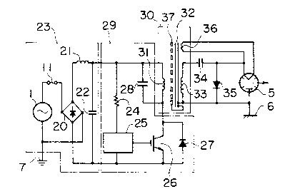
A circuit diagram of a high-frequency heating apparatus
according to an embodiment of the present invention is shown
in Fig. 2.
In Fig. 2, a commercial power supply 1, a fuse 11, a
diode bridge 20, an inductor 21 and a capacitor 22 make up a
power supply unit 23 to constitute a unidirectional power
supply. The power is supplied to a control circuit 25
through a resistor 24, which subjects a transistor 26 to a
switching operation at a high frequency of, say, 20 kHz to 1
MHz. Numeral 27 designates a diode and numeral 28 a resonant
capacitor. The diode 27 and the capacitor 28 constitute a
resonance-type inverter (frequency converter) 29. Thus, the
primary winding 31 of the boosting transformer 30 is supplied
with high-frequency power of the same frequency as the
switching frequency of the transistor 26, thereby generating
a high-voltage output across the secondary winding 33
magnetically coupled through the core 32. This output is
rectified by a capacitor 34 and a diode 35 and is supplied to
a magnetron S. Since the cathode of the magnetron 5 is
heated by a heater coil 36, the magetron 5 is oscillated and
a microwave output is generated to permit dielectric heating.
The resonance-type inverter 29, the detailed operation of
which is well known and will not be described, is what is
called a one-transistor inverter of the voltage resonance
type. The current Ic flowing in the
2~ 467
1 transistor 26 is thus a collector current in triangular
form, and the collector voltage VCE is a resonance
voltage in sinusoidal form. A high-frequency voltage
equal to the switching frequency of the transistor 26 is
generated between the terminals of the primary winding
31 of the boosting transformer 30.
A shield member 37 is arranged at a position
near to the primary winding 31 between the same primary
winding 31 and the secondary winding 33 and the heater
winding 36 of the boosting transformer 30. This shield
member 37 is connected to a core 32 which in ~urn is
- connected substantially to a housing 6 of ~ lgh-
frequency heating apparatus.
As a result, the high-voltage circuit on the
output side of the high-voltage secondary winding 33 is
substantially contained in the shield space of the same
potential as the housing 6 by the presence of the shield
member 37. In case of a fault of the high-voltage
secondary winding, leading to ~ dielectric breakdown,
therefore, it is possible to prevent what is called the
mixed contact between the primary and secondary windings
by contact with the primary winding 31. Especially, the
- boosting transformer 30 is adapted to increase the
output voltage of the resonance-type inverter 29 and is
so compact that the shield member 37 may well be simple
in construction and compact, thus greatly facilitating
the containment of the high-voltage circuit within the
shield space.
20Q0467
A sectional view of the construction of the boosting
transformer 30 is shown in Fig. 3. In Fig. 3, the component
elements designated by the same reference numerals as those
in Fig. 2 provide the corresponding component elements and
will not be described in detail below. The shield member 37
is mounted on a bobbin 40 of the primary winding 31 in the
manner shown for shielding the secondary winding 33 through
the space layer 42 between the secondary winding 33 and the
bobbin 41. This shield member 37 is connected to the core 32
at the inner diameter portion 43 thereof and further to the
housing 6 by a lead wire 44.
This construction shields the secondary winding 33 and
the heater winding 36 from the primary winding 31 and
prevents the potential of the housing 6 from increasing to an
abnormally high level with the primary winding 31 mixed and
brought into contact with the secondary winding 33 even if
the secondary winding 33 runs out of order and insulation
breaks down for some reason. As a result, the need for
grounding the housing 6 further by a ground line is
eliminated, thereby providing a safe high-frequency heating
apparatus convenient to operate.
The shield member 37 is indispensably interposed between
the primary winding 31 and the secondary winding 33 as shown,
and therefore the adverse effect of the high-frequency
magnetic fluxes generated by them increases unavoidably.
~ 8
- 2()nQ467
1 Fig. 4 is a diagram showing an embodiment of
the construction of the shield member 37 for preventing
the adverse effect of the high-frequency magnetic
fluxes. As shown, the shield member 37 is constructed
of a reticular wire material with a slit e as shown.
This construction will be described later again. The
wire material may be stainless steel, brass, aluminum or
the like non-magnetic metal, although stainless steel is
best suited for its induction heating characteristic and
lo mechanical strength.
This wire material is configured in reticular
form as shown in the enlarged view of Fig. 5. Wire
members, which are in contact with each other at a small
point, have a high resistance against the high-frequency
electromagnetic induction voltage. As a result, the
adverse effect of the high-frequency magnetic fluxes
caused by the primary winding, that is, the phenomenon
of what is called the induction heating caused by
partial induction of an eddy current in the shield
member is minimized, thus preventing the inconveniences
which otherwise might be caused by the shield member
being abnormally increased in temperature and while at
the same time preventing the total loss of the boosting
transformer from being increased. Further, the
substantial shielding between the primary and secondary
windings is assured by maintaining the relationship of
mesh size shown in Fig. 6. Specifically, assuming that
the wire interval (mesh size) of the shield member 37 is
- 2()nO467
1 2el and the distance between the shield member 37 and
the primary winding 31 (thickness of the flange 40a of
the bobbin 40 in the present embodiment) is e2, the
relationship e1 < e2 is assured in construction. It is
thus possible to realize a substantially sufficient
shield between the primary and secondary windings even
by a reticular shield member 37.
This reticular configuration is realized not
necessarily by a netting of wire material but may be
obtained by a construction similar thereto. Specifical-
ly, depending on the frequency of the inverter or the
arrangement of the shield member 37, the effect equiva-
lent to the reticular shield member is realized by a
punched metal or a construction like the shadow mask of
15_t~ff~cathode ray tube. In other words, it is possible to
use a shield member of such a construction that the
resistance value against the high-frequency electro-
magnetic induction voltage can be sufficiently increased
in practical fashion.
A shield member 37 in this reticular form or
having a construction similar thereto is provided with a
slit e as shown in Fig. 4, for the reason mentioned
below. As explained with reference to Fig. 5, the
current induced in each part of the shield member 37 by
the magnetic fluxes generated through the primary
winding may be minimized by a reticular or a similar
construction. In the absence of the slit e, however,
the collective induction current indicated by the arrow
-- 10 --
20Q0467
in Fig. 4 would flow away along the direction of w;n~;~g of
the primary 31. As evident from Fig. 3, the provision of the
shield member 37 between the primary winding 31 and the
secondary w; n~; ng 33 inevitably causes an induction current
to flow in the shield member 37 by the magnetic fluxes
induced by the primary winding 31. Even if the reticular
shield member 37 is constructed as shown in an embodiment of
the present invention, the collective induction current
thereof would inevitably flow in the direction shown by the
arrow in Fig. 4, thus subjecting the shield member 37 to
induction heating. If the slit e is formed to construct the
shield member 37 in a substantially electrically open loop
with respect to the direction of winding of the primary,
however, the shield member is prevented from being heated by
induction with the collective induction current flowing as
mentioned above.
The width of this slit e may be designed by a concept
similar to the size of mesh (2 e 1) described with reference
to Fig. 6. It is thus possible to shield the primary winding
31 and the secondary winding 33 substantially from each other
even in the presence of the slit e.
Experiments conducted by the inventors show that when an
inverter of several tens to several hundreds of kHz is
involved, the use of a shield member made of an SUS 304
reticular material of about 30 meshes and having a slit e of
X 11
20Q0467
approximately 1 mm as shown in Fig. 4 can substantially
eliminate the temperature increase of the shield member by
induction heating.
A construction of the shield member 37 according to
another embodiment of the invention is shown in Figs. 7A-7C.
In the case where the boosting transformer has a very
few number of turns of the primary winding 31, for example, a
considerable induction voltage is generated in the slit e,
thereby making it impossible to reduce the slit e
sufficiently in the embodiment of Fig. 4.
If a pair of shield members 37a, 37b shown in Figs. 7A
and 7B are arranged with a sufficient insulation distance g
in the manner shown in Fig. 7C, on the other hand, the
primary winding 31 and the secondary winding 33 are
substantially shielded from each other with sufficiently
large slits ea and eb-
The construction of still another embodiment of the
shield member 37 is shown in Figs. 8A and 8B.
In Figs. 8A and 8B, a circular shield member 37 is
comprised of shield plates 52, 53 and an insulating layer 54
made of insulating paper or the like. The shield plates 52,
S3 are made of such material as stainless steel, aluminum or
copper and have a plurality of grooves 50 equidistantly
arranged in a radial direction and a slit 51 for constituting
an electrical open loop in the winding direction of the
winding of the primary (along the arrow in the drawing). In
2000467
the present embodiment, the two insulating plates 52 and 53
have exactly the identical shape, and the width ~3 of the
groove 50 is determined to be smaller than one half of the
interval e4. The insulating plates 52 and 53 are arranged
in such relative positions that the center line Pl of the
groove 50 of the shield plate 52 is displaced by an angle e
from the center line P2 of the groove 55 of the shield plate
53 as shown. Specifically, all the grooves 50 and 55 are
arranged in such a manner as to be covered by grooveless
portions through the insulating layer 54. As a result, the
shield member 37, when viewed vertically in Fig. 8B, would be
totally lacking in openings other than the hole 56 for
passing the core 32 even in the absence of the insulating
layer 54. If an opening exists in this direction, an
inconvenience mentioned below would result. Specifically, as
shown in Fig. 9, assume that the bobbin 41 of the secondary
winding 33 has the flange 57 thereof molten. The part 58 of
the secondary winding may approach the primary winding 31
through the opening 59 of the shield member 37 and cause what
is called the mixed contact of the primary and secondary
windings. This would be a very dangerous condition.
According to the embodiment of the present invention,
however, the shield member 37 totally eliminates the opening
59 between the primary and secondary windings and the adverse
effect of the high-frequency magnetic fluxes is prevented.
Specifically, the grooves 50 shown in Fig. 8A are formed
together with a slit 51 to constitute an electrical open loop
20Q0467
in the direction of winding of the primary, so that what is
called the induction current is minimized, thus greatly
reducing the loss occurring at the particular point. The
core 32 is made of ferrite and the shield plate 52 is
constructed of a non-magnetic stainless steel of about 0.5 mm
or thinner. By doing so, even in the case where the power of
a frequency of about 100 kHz is increased in voltage, the
loss of the shield plate 52 is kept very small. The fact
that the grooves 50 and the slit 51 are formed in the
direction crossing the winding of the primary as mentioned
above increases the resistance to the substantial high-
frequency induction voltage and thus greatly reduces the
high-frequency induction loss. A similar construction is of
course realizable also by use of other materials. For
example, the insulating layer 54 may be formed of a ceramic
sheet or insulating paper, and conductive films in the shape
of the shield plates 52, 53 are printed on the surface of the
ceramic or the like sheet with equal effect.
Figs. lOA and lOB show a partial plan view and a front
view respectively of a shield member 37 including three
shield plates 52a, 52b, 52c which are insulated by two
insulating layers 54a, 54b. These shield plates 52a to 52c
are shaped exactly the same way as the shield plate 52 shown
in Figs. 8A and 8B. As is clear from Fig. lOA, however, the
grooves of the shield plates 52a to 52c have a greater width
(corresponding to the length ~3 in Fig. 8A). As a result, as
shown in the sectional view of Fig. lOB, three shield plates
2~46?
are superimposed through the insulating layers 54a, 54b, and
at the same time as shown in Fig. lOA, the grooves are
displaced slightly from each other thereby to constitute a
shield member 37 substantially free of an opening as a whole.
A partial sectional view of the boosting transformer 30
according to another embodiment of the invention is shown in
Fig. 11, in which the component parts equivalent to those in
Figs. 3 and 8A and 8B are designated by the same reference
numerals respectively as in Figs. 3 and 8A and 8B. This-
boosting transformer 30 comprises a core 32, a bobbing 41 of
the secon~ry winding 33 mounted on the core 32, an
insulating cylinder 60, a shield member 37 including shield
plates 52, 53 and an insulating layer 54 on the outside of
the insulating cylinder 60, and a bobbin 40 with the primary
winding 31 on the outermost side. The shield plates 52, 53
have grooves 50 shown in Fig. 12A or 12B and a slit 51 formed
as shown in Fig. 12C, which is a diagram of the shield plate
52 having the grooves 50. If shield plates like those
designated by 52 in the shown shape with different inner
diameters are provided, the shield member 37 shown in Fig. 11is constructed. The shield plates 52 and 53 are arranged in
such relative positions that the grooves 50 thereof are not
overlaid on each other, resulting in the same function and
effect as the embodiments explained with reference to Figs. 3
and 8A and 8B. Similar
~ 15
~onQ467
-
1 function and effect are of course obtained by
configuring the shield plate 52 in the shape shown in
Fig. 12C of a non-magnetic conductive material in
reticular form or having equivalent characteristics as
shown in Fig. 5.
Figs. 13A and 13B show a plan view and a
sectional view respectively of a further embodiment of
the shield member 37. This embodiment is applicable to
the boosting transformer 30 shown in Fig. 3.
In the configuration of this embodiment, a
pair of non-magnetic metal members 60 of copper or
aluminum is covered with an insulating material 61.
Each metal member 60 is basically U-shaped and includes
two parallel conductor parts in opposed relations to
each other with an end open and the other end short-
circuited. A couple of metal members 60 are arranged
concentrically, each having a grounding connector
terminal 62.
The maximum distance 2~between the metal
conductors is set smaller than the minimum distance e2
between the primary and secondary windings.
The metal members 60 making up a shield member
have also slits 63, 64. The embodiment under consider-
ation is provided with two of such slits.
The metal member 60 may alternatively be
constructed as shown in Fig. 14. Specifically, a
multiplicity of U-shaped metal members 60 are arranged
not along the circumference but in~radial direction with
- 16 -
20~C~467
.,
1 the shortcircuited U-shaped ends integrated along the
circumferential direction, while portions thereof are
cut off to form slits 63, 64. This configuration thus
resembles that of the embodiment shown in Fig. 8A.
Aside from this configuration, a configuration as shown
in Fig. 14 is also possible. Further, a plurality of
shield members 37 shown in Figs. 13 and 14 may be
superposed as required.
In view of the basically U-shaped construction
,~ 10 of the metal conductors 60 with the slits 63 and 64 as
described above, currents offsetting each other flow in
the two parallel wires, so that the current inAloop is
substantially reduced, thereby preventing the loss due
to heat generation of the metal members 60 or inconveni-
ent operations which otherwise might be caused by the
magnetic fluxes between the primary and secondary
windings.
As explained above, according to the present
invention, the output of a frequency converter is
supplied to a magnetron by increasing the voltage
thereof through a boosting transformer, a shield member
of non-magnetic conductive material substantially
W~ ~6-
forming an electrical open loop in theAdirection of ~C~
primary winding is inserted between the primary and
secondary windings of the boosting transformer, and a
part of the shield member is connected to a core or a
housing of the boosting transformer. The compact high-
voltage parts of the boosting transformer and the like
- 17 -
20Q04~7
realizes shield means easily between the primary and
s~co~ry windings with a very simple construction, thus
making it possible to contain the high-voltage circuit within
a shield space. The need of y~l..7i~g the housing is
eliminated while assuring a sufficiently high safety. As a
result, a high-frequency heating apparatus is realized which
eliminates the need of grounding, free to carry and
convenient to operate. In particular, the aforementioned
configuration of the shield member completely prevents the
shield member from being subjected to induction heating by
high-frequency magnetic fluxes, leading to a great power
loss, or from being burned by overheat. ThAnk~ to the
elimination of the ylo~ 7; ng work and the great operating
convenience, a high-frequency heating apparatus with high
safety and high efficiency is realized.
on the other hand, a shield plate consisting of a
netting or in reticular construction having a resistance
equivalent to the netting against a high-frequency induction
voltage, is used to realize easily a shield member which is
very low in cost. Further, if a shield member is constituted
by a shield plate having a plurality of grooves crossing the
winding direction of the primary winding, the shield member
is very easily and conveniently produced at low cost for
practical purposes. In addition, by arranging a plurality of
shield plates in such relative positions that the grooves are
not superposed on one another, a shield member completely
~ 18
- 200C~4~7
1 free of an opening between the primary and secondary
windings is realized, thus assuring complete safety.
Furthermore, the U-shaped configuration of the
two conductors arranged in substantially parallel
relations realizes the cancellation of voltages induced
by the high-frequency magnetic fluxes with each other,
and therefore the induction current is completely offset
and prevented from flowing.
The configuration of the shield member covered
with an insulating member facilitates the packaging of
the shield member on the boosting transformer. In view
of the simplicity of the voltage-withholding design of
the shield plate and the high-voltage portions, for
instance, there is no need of enlarging the insulation
distance, thereby making it possible to reduce the whole
size of the boosting transformer.
In addition, if a shield member is made up of
a non-magnetic conductive material printed, attached or
deposited by evaporation on the surface of the ceramic
or the insulation paper, the mass-productivity thereof
is greatly improved. Still another advantage is a high
processing accuracy in multilayered construction or fine
structure of the grooves.
-- 19 --