Note: Descriptions are shown in the official language in which they were submitted.
2~00~7~
DIGITAL GMSK MODULATOR WITH NON-
INTEGER BIT INTERVAL HANDLING
10 Field of the Invention -
The present invention relates generally to radio frequency
(RF) circuits, and, more particularly, to RF modulation circuits.
Brief Descril)tion of the Drawin~s
Fig. 1 is a block diagram of a modulation arrangement
kno~,vn in the prior art;
25Fig. 2 is a block diagram of a modulation arrangement,
according to the present invention;
App. A is a C language program useful for generating the
contents of the ROMs 210 and 212 of Figure 2;
App. B is a state diagram representing the operation of the
30quadrant register 230 of Eigure 2; and
App. C is a state diagram representing the operation of the
quarter bit register 240 of Figure 2.
..... ~ .. . . . . .. . . .
::
.
. .. .. :
.
.. .
lA
2~4 7~
15 Backgroun~ Art
Gaussian Minimum Shift Keying (GMSK) modulation can
be generated digitally by employing ROM (read only memory)
look-up tables, or a combination of random logic and ROM look-up
20 tables, using digital FIR (Finite Impulse Response) techniqu~s.
This is typically accomplished in an RF system by programming
two ROMs with data to accommodate FIR filtering functions, one
ROM programmed to produce the I channel component and the
second ROM programmed to produce the Q channel component of
25 the baseband GMSK signal. Figure 1 illustrates this known
approach. For more details on this modulation technique,
reference may be made to H. Suzuki et al., "3ingle-Chip Baseband
Waveform Generator CMOS-LSI for Quadrature-Type GMSK
Modulator," Electronic Letters, 11 October 1984, Vol. 20, No. 21,
30 pp. 875-876, which discloses a diagram representative of that
shown herein in Figure 1. Additional background information of
frequency shift keying, e.g., MSK or GMSK,
modulation/demodulation systems may be obtained by
referencing U.S. Patents 4,606,051- Crabtree; 4,414,675 - Comroe;
. ~- . . -
.
. :
:~
. .
,
- 2 - CE00118R
and 4,581,749 - Carney et al, all of which are assigned to Motorola,
Inc. Reference may also be made to M. Simon and C. Wang, "Bit
Synchronization of Differentially Detected MSK and GMSK,"
IEEE International Conference on Communications, June 1985,
5 pp. 583-590; and K. Murota and K. Hirade, "GMSK Modulation for
Digital Mobile Radio Telephony" IEEE Transactions on
Communications, Vol. COM-29, No. 7, July, 1981, pp. 1044-1050.
For information on digital phase modulation techniques using
ROMs, reference may be made to John B. Anderson, Tor Aulin
10 and Carl-Erik Sundberg, "Digital Phase Modulation, " Plenum
Press, New York, NY, 1986, pp. 211-235.
Such a techni~ue works well with data being clocked out
regularly on one bit intervals. However, there are times when the
data has to be clocked for an interval greater than one bit ~e.g.,
15 1.25 bit). This rnay occur, for example, in TDMA (time division
multiple access) systems which has time slots which contain a
non-integer number of bits.
Theoretically, such a requirement would not cause a
splatter in the transmission frequency spectrum since the data
20 rate is lowered at such irregular times. However, the fractional
bit interval causes a phase discontinuity in the ROM look-up table
output. For this reason, known systems using the approach of
Figure 1 cannot be employed to accommodate such a
requirement.
Objects of the Invention
It is therefore a general object of the present invention to
provide a digital modulation technique which overcomes the
30 above mentioned shortcomings.
It is a more specific object of the present invention to
provide a digital modulation technique which provides digital
GMSK or any digital frequency modulation with non-integer bit
interval capability.
. : ,
- .
---- 20~a~7~
- 3- CE00118R
The present invention may briefly be described in terms of a
preferred embodiment. Essentialiy, a modulation circuit is used
in a modulation system substantially synchronized to a system
clock. The system includes one or more ROMs, each ROM being
5 preprogrammed as a look-up table for generating a representative
digital waveform based on an integer bit interval input data
stream and a clock signal. Each digital waveform is converted to
an analog signal for subsequent radio frequency (RF) modulation.
Each ROM is addressed by an interpolation counter controlled by
10 the clock signal, by a data shif~ register receiving input data at a
rate corresponding to the clock signal, and by a quadrant register,
also receiving the input data, for specifying the phase of the data
signal with respect to the clock signal. Additionally, a signal that
indicates the presence of a non-integer bit interval is provided. In
15 response to this signsl, ROM addressing is updated in order to
avoid phase discontinuity at the look-up table outputs.
Accordingly, a method of maintaining the phase of a modulated
carrier signal based on the introduction of a non-integer bit
interval is achieved.
-. . , :
.
- ,
- . ~. -
47'~5
- 4 - CE00118R
Detailed Description of the Preferred Embo~iment
The arrangement disclosed in this specification is directed
to GMSK signalling in an RF cellular radiotelephone
5 communication system. More specifically, the instant invention
is best used in a digitally generated GMSK signalling technique
which allows data to be clocked into the signaling protocol at
irregular non-integer intervals, e.g., at one quarter bit intervals.
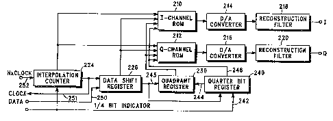
~ig. 2 illustrates a general block diagram of an
1 0 arrangement which embodies the instant invention. The
arrangement of Figure 2 is similar to the known arrangement of
Figure 1, but it includes an improvement to accommodate the
signalling protocol at irregular non-integer intervals, as
previously discussed. Common to both arrangements of Figures
1 5 1 and 2 are conventional 2048-byte ROMs 110/112 and 8192-byte
ROMs 210/212, digital to analog (D/A~ converters 114/116 and
214/216 such as a TDC1016 available from TWA, Inc.,
reconstruction filters 118/120 and 218/220 (preferably conventional
Bessel low pass filters), interpolation counters 124 and 224 such
20 as a conventional divide-by-N ripple counter, M-bit shift reg~sters
126 and 226 having parallel data output, and quadrant registers
130 and 230 such as conventional 2-bit up/down counter. Unique
to the arrangement of Figure 2 i9 a quarter-bit register 240, its
associated 1/4 bit indicator 242 and data 243, its quadrant register
25 output 244 and its ROM address outputs 246.
Preferably, a 2-bit up/down counter is used to implement
the quarter-bit register 240.
The operation of the arrangement of Figure 2 will now be
discussed in block diagram form using references to conventional
30 counters and shift registers to facilitate discussion. This
discussion will be followed with a state operational discussion of
the quadrant register 23û and the quarter bit register 240 for more
specific explanation.
.
:
~. . .
2~ 75
- ~- CE00118R
The I- and Q- channel ROMs 210 and 212 are
preprogrammed with data using a C language program,
attached as appendix A. This program provides the data for the
ROMs to serve four functions: (1) a digital FIR tFinite Impulse
5 Response) filter, (2) and integration process, (3) phase correlation
for sine and cosine processing of the I- and Q- channel
components of the input data, and (4) NRZ (nonreturn-to-zero) to
impulse conversation. Because GMSK modulation can be
generated digitally by a digital FIR (Finite Impulse Response)
1 0 filter, the FIR function is incorporated into the preprogrammed
ROM data to approximate the required Gaussian data filter with
NRZ data input and the phase ang~le output. The phase angle
output is then used in conjunction with a SIN (sine) and a COS
- (cosine) portion of the respective ROM look-up tables to generate
1 5 the I- and Q- channel baseband components in digital form.
The D/A converters 214 and 216 are used to convert the data
output from the ROMs 210 and 212 to the I- and Q-channel
baseband components in analog. form. Conventional
reconstruction filters 218 and 220 are then employed before the
20 quadrature modulation step.
The interpolation counter 224 provides the interpolation
filtering (oversampling) control for the ROMs 210 and 212 by
addressing the ROMs 21~ and 212 using its counter outputs. The
interpolation counter 224 is used to ease the reconstruction filter
25 design for anti-aliasing and sin~/x correction. The interpolation
counter 224 is driven by a clock signal 252 operating at a rate of N
times C, where C is the clock rate at which data is to be
transmitted through the system and N is determined so that
there is an adequate number of samples to represent a bit.
30 Functioning as a divide-by-N counter, the output of the
- interpolation counter 251 is a clock signal operating at rate C.
This output i9 connected to the data shift register 226 to clock data
- 250 therein, and connected to data source circuitry (not shown) so
,
.- - -
- . . ~.
,
, . : - . .
- 2~n~3~7s
- 6- CE00118R
as to provide the rate at which data is to be received by the data
shift register 226.
The data shift register 226 rece*es the data 250 in serial
form and provides address signals to the ROMs 210 and 212
5 according to the program attached in appendix A in order for the
ROMs to provide its representation in I- and Q- channel
component form. The length of the data shift register 226 is
deterInined to be greater than or equal to the duration of the FIR
impulse response. In the illustrated embodiment, the length of
1 0 the data shift register 226 is 5 bits.
The quadrant register 230 receives the data shifted out of
the data shift register 226, and is used to inform the ROMs 210
and 212 of the phase angle of the data 250 for the phase angle
calculation in the integration process of the program of appendix
1 5 A. Because the program integrates in conjunction with the phase
angle calculation, the calculation result may go beyond 0 to 360
degrees. Since the ~MSK may be viewed as a Gaussian data filter
followed by an FSK (frequency shift key) modulation with a
modulation index of 0.5, i.e., the phase change due to FSK is
20 always plus or minus 90 degrees at the end of a bit interval, a 2 bit
quadrant register is sufficient to represent 1 of the 4 possible
quadrants as a result of the integration process. When the energy
of a modulation bit ripples through the FIR, the quadrant register
230 is incremented or decremented accordingly and the ROM
25 look-up table can be restarted with a new bit shifted in.
A non-integer bit (functional-bit) register 240, a quarter bit
register in the illustrated embodiment, is introduced to handle
irregular (unpredicted or aperiodic with respect to the clock rate
C) data synchronization. This may occur in systems which
30 require resynchronization for access transmission, e.g.,
resynchronization to a system clock in a TDMA (time division
multiple access) system.
The quarter bit register 240 handles such irregularity by
adjusting the addresses of the ROMs which specify the phase of
,.. .
. ~:
, . ... .
.: ~
,
475
- 7- CE00118R
the data signal. More specifically, this is accomplished by
coupling the data lead 243 to the up/down port of the counter used
to implement the quarter bit register 240, by clocking and
enabling the quarter bit register 240 only upon reception of an
external quarter bit indicator signal along 242, and by coupling
the overflow bit 244 of tha register 240 to the up/down port of the
quadrant register 230. The V4 bit indicator 242 is coupled to the
interpolation counter 224 in order to restart its counting process.
The restarting of the counting process is necessary in systems
1 0 which require resynchronization with the such irregular non-
integer bit times. The output 246 of the quarter bit register 240
addresses the ROMs 210 and 212 according to the specification of
the program of appendix A.
Using 1/4 bit incrementation as an example, a two bit
1 5 register or counter may be used in the implementation of the
quarter-bit register 240.
It should be noted that the data shift register 226 should
contain all l'1"s or all "0"s before the V4 bit indicator activates so
that the FIR portion of the circuit is in a steady state mode.
Appendix B illustrates a state diagram of the quadrant
register 230. There are four states which represent this operation
and 3 conditions to which the states react. Each state represents
a steady state condition of the quadrant register 230. Condition
"A" occurs when the output of the data shift register is high and
the interpolation counter 224 has reached 15 (counting from 0 to
15); or the output of the data shift register is high and the outputs
of the quarter bit register 240 represent "3" (highest count from 0
to 3 of a 2 bit counter) and the 1/4 bit indicator 242 is high.
Condition "B" occurs when the output of the data shift register is
low and the interpolation counter 224 has reached 16 ~counting
from 0 to 15); or the output of the data shift register is low and the
outputs of the quarter bit register 240 represent "0" (lowest count
from 0 to 3 of a 2 bit counter) and the V4 bit indicator 242 is high.
The "else" condition represents all other conditions.
1' . ~ . . - ~, .
..
.. ..
,, ~ , ..
. .. ..
- . .
;~n~347s
- 8- CE00118R
Appendix C ;llustrates a state diagram of the quarter bit
register 240. There are four states which represent this operation
and 3 conditions to which the states react. Each state represents
a steady state condition of the quarter bit register 240. Condition
5 "A" occurs when the output of the data shift register is high and
the 1/4 bit indicator 242 is high. Condition "B" occurs when the
output of the data shift register is low and the 1/4 bit indicator 242
is high. The "else" condition represents all other conditions.
. . . ~ . .
.
.
.
'
'~
n ~3475
APPENDI X A
,~ I QUADRATURE MODULATOR. EL BASEBAND WAYEFORM FOR ~/
#DEFINE RECORD_LENGTH 32 /~3YTES PER DOWNLOADING LINE ~/
#DEFINE ADDR_WIDTH 13 /~NUUaER OF ADDRESS BITS */
#DEFINE SR_LENGTH 5 /*LENGTH OF SHIFT REG ~/
#DEFINE COUNTER_LENGTH 4 /*LENGTH OF CQUNTER */
#DEFINE INTERPOLATION FACTOR 16
#DEFINE START_ADDRESS O /t DOWNLOAD START ADDRESS */
$DEFINE PULSE_SHAPE GAUSSIAN
#DEFINE CONVRSION TRIG /*'NULL' FOR PSK */
~DEFINE COMPONENT SIN /~I CHANNEL ~/
#DEFINE OFFSET O /~'1' FOR OQPSK ~/
#DEFINE BT 0.30 /*BT PRODUCT FOR GASSIAN LPF ~/
#DEFINE DA 3IT 8 /*D/A RESOLUTION */
#DEFINE OUTPUT_FORMAT s19 /tpROGRAMMER DOWNLOAD FOR~AT*/
#DEFINE QRI 10 /*ADDRESS LINE FOR QRl */
tDEFINE QRO 9 /J ADDRESS LINE FOR QRO */
#DEFINE QB1 12 /*ADDRESS LINE FOR QBl */
#DEFINE QBO 11 /~ADDRESS LINE FOR QBO */
/* GLOBAL VARIABLES ~/
UNSIGNED LONG INT ROM_SI7E;
INT BIT[15];
INT INVERT~15] = ~1,0,0,0,0,0,0,0,0,0,0,0,0,0,0,~;
/* BIT[O] WILL BE INVERTED FOR EPROM */
INT TIME[] = {0,1,2,3~;
INT SR[] = ~4,5,6,7,8};
GOUBLE SYMBOL [SR_LENGTH] [INTERPOLATION_FACTOR];
$INCLUDE <STDIO.H>
#INCLUDE <MATH.H>
$INCLUDE "GAUSSIAN.H"
#INCLUDE "sl9.H"
#INCLUDE "MODULATOR.H"
#DEFINE RECORD LENGTH 32 /*BYTES PER DOWNLOADING LINE */
#DEFINE ADDR_WIDTH 13 /t NUUBER OF ADDRESS BITS */
#DEFINE SR_LENGTH 5 /~LENGTH OF SHIFT REG */
#DEFINE COUNTER_LENGTH 4 /*LENGTH OF COUNTER */
#DEFINE INTERPOLATION FACTOR 16
#DEFINE START_ADDRESS O /~DOWNLOAD START ADDRESS */
#DEFINE PULSE SHAPE GAUSSIAN
#DEFINE CONVERSION TRIG /~'NULL' FOR PSK */
$DEFINE COMPONENT COS /~Q CHANNEL */
#DEFINE OFFSET O /~'1' FOR OQPSK */
#DEFINE BT 0.30 /*BT PRODUCT FOR GASSIAN LPF */
#DEFINE DA_BIT 8 /~D/A RESOLUTION */
~DEFINE OUTPUT_FOR4AT sl~ /-PROGRAM-ER DOWNLOAD FOR~AT`/
~n~ 7s
APPENDI X A
#DEFINE QR1 lO /~ADDRESS LINE FOR QR1 ~/
#DEFINE QRO 9 /*ADDRESS LINE FOR QRO ~/
~DEFINE QBl 12 /~ADDRESS LINE FOR QBl */
tDEFINE QBO ll /~ADDRESS LINE FOR QBO */
/~ GLOaAL VARIA3LES ~/
UNSIGNED LONG INT RO~_SIZE;
INT PIT[15];
INT INVERT[15] = ~1,0,0,0,0,0,0,0,0,0,0,0,0,0,0,~;
/~ BIT[O] WILL BE INVERTED ~/
INT TIME[] = ~0,1,2,3};
INT SR[] = ~4,5,6,7,8};
DOU3LE SYMBOL [SR_LENGTH] ~INTERPOLATION_FACTOR];
#INCLUDE <STDIO.H>
#INCLUDE <MATH.H>
#INCLUDE "GAUSSIAN.H"
#INCLUSE "sl9.H"
$INCLUDE "MODULATOR.H"
/~ GAUSSIAN.H MODULE TO 3E INCLUDED 3Y MAIN MODULE. ~/
/~ TO GENERATE AN ISOLATED, GAUSSIAN LOW PASSED, NRZ ~/
/~ OUTPUT SYMBOL. COUNTER LENGTH, SR LENGTH AND BT CONSTANT ~/
/~ FOR THE GAUSSIAN LPF ~RE DEFINED~IN THE MAIN MODULE. t/
/~ OUTPUT WAVEFORU IS STORED IN AN EXTERNALLY DEFINED ARRAY ~/
/~ CALLED SYM90L[N][T]. ~/
GAUSSIAN(SR LEN, INTERPOLATION, BT)
INT SR_LEN,-INTERPOLATION;
DOUBLE BT;
DOUBLE S, OFFSET;
DOU3LE K1,K2,K3,K~
DOU~LE A1,A2,A3,A4;
INT N, T;
K1 = 0.785398163397~8;
K2 - 5.336446257 ~ BT;
K3 = 0.0830353088 / BT;
K~ = 28.47765865 ~ BT ~ BT;
OFFSET = SR LEN / 2;
FOR (N=O; N< SR LEN; N++) ~
FOR (T=O, T< INTERP~LATION; T++)
S=((DOUBLE)T) / INTERPOLAT~ION
+ ((DOUBLE)N) = OFFSET;
A1 = (S+~.5) ~ ERF (K2 ~ (S=0.5));
A2 = (S=0.5) * ERF (K2 ~ (S-0.5));
A3 = EXP(K4 * (S+0.5) * (S+0.5));
A~ = EXP(K~ ~ (S-0.5) * (S-0.5)):
~- SYMBOL[N][T] = K1 ~ (1+A1-A2) + K3 * (A3-A4);
}
/* sl9.H MODULE TO BE INCLUDED BY THE MAIN MODULE.
sl9 (ADDRESS, DATA) /~ GENERATE S19 RECORDS ~/
UNSI~NED LONG INT ADDRESS;
UNSIGNED INT DATA;
- ' .
.
r~4175
A PPENDI X A
EXTERN UNSIGNED LONG INT ROM SIZE;
STATIC INT BYTE COUNT = REC~RD LENGTH;
STATIC UNSIGNED-INT CHECKSUM = 0;
(( pRRETSFS ,,sl,,lART_ADDRESS) X RECORD LENGTH -=O) }
BYTE COlNT = RO~ SIZE = ADDRESS;
IF ~B-YTETCOUNT > REC~RD_LENGTH) BYTE_COUNT = RECORD_LENGTH;
PRINT4H ~ADDRESS);
CHECKSUM = BYTE_COUNT + 3 + ADDRESS X 256 + ADDRESS /256;
CHECKSU~ = CHECKSUM + DATA;
BYTE COUNT--; -
PRINT2H (DATA);
IF (BYTE_COUNT == 0) ~
CHECKSUV = 255 - CHECKSUM X 256;
PRINT2H (CHECKSUM);
PRINTF ("\N");
} IF (ADDRESS + 1 =- ROM_SIZE) PRINTF("S9030000FC~N");
IPNRINT2H(X) /* PRINT X AS TWO HEX DIGITS */
-UNsAIGINcEcHANRT HyEX[] = 0l23456789A8CDEFll;
r = X/16;
ELS~ ~ ¦ ¦ Y < 0) PRINTF ("?")
} PUTCHAR(HEX~Y]);
Y = X % 16;
RETURN; ( ~ ]);
IPNRTNTX4H (X) /* PRINT X AS FOUR HEX DIGITS ~/
UNSIGNED INT Y-
IF ~X~> 65535 ~ ¦ X < 0) PRINTF("??~?");
Y = X / 256;
PRINT2H (Y)-
Y = X % zg6;
PRINT2H (Y);
} RETURN;
/~ MODULATOR.H ~ODULE TO BE INCLUDED 8Y THE ~AIN ~ODULE. ~/
/* THIS IS DESIGNED FQR THE GENERIC QUADRATURE UODULATOR. */
/* ALL PREPROCESSOR STATEMENTS ARE DEFINED IN THE ~.C FILE. */
/* REVISION HISTORY: ~/
/~ 12/05/86 FIRST CREATED ~/
/~ 02/18/87 MODIFIED FOR REVERSING SHIFT REGISTER ~/
/~ 5/26~88 TRIG(X) MODIFIED FOR QUARTER BIT ~/
/~ 7/01/88 ADD INVERT~15] MASK FOR INVERTED INPUT */
/* TO EPROM. RE~UIRED TO SUPPORT GDB ~/
/~ TIMING. ~/
UGN5IGN ~X~ /~ CONVERT X TO 0INARY IN BIT~] ~/
. Il
. . ~
. .
.. - :
. . .
,'~ ~ ': '' '
- . .
-:
:: .
Z~l~rJ475
APPENDI X A
EXTERN INT BITrl51;
IXTEIN INT INVER~ ~15];
FOR (I=O; I<16; I++) ~
BIT I = X ~ 2
BIT X ; ~BIT [I~ ^ INVERT ~I];
DOUBLE ECHO(ADDRESS) /~ CONVOLUTION PROCESS ~/
LONG INT 3IT[t5];
EXTERN INT aIT~151,
EXTERN DOUBLE Y OL[SR_EENGTH] [INTERPOLATION_FACTOR];
DOUBLE Y;
GETBIN (ADDRESS);
T - BIY[5] ^ OFF~ET; ]
FOR (I = COUNTER_LENGTH -2; I>= O; I--)
J = TI~E[I];
} T = T ~ 2 + BIT~J];
Y = O;
FOR (I = O; 1 < ~S~_LENGTH; I+~) ~
~ Y = Y + (2 t ((DOUBLE)BIT[J]) ~ SYMBOL~I]~T];
} RETURN (Y);
Do8BtE X; ( ) /~ NULL FUNCTION FOR QPSK OR OQPSK ~/
RETURN(X);
DoOu8tEE TRIG(X) /~ PHASE TO I/Q CONVERSION FOR ~SK AND GMSK ~/
EXTERNAL BIT~151
IN$ B, BO B1 B3'14B5392653S8979323846;
BO = BIT~QBO];
B1 = BIT~QB11-
B2 = BI~QR~
B3 = BIT[QRlr;
X - X + B * P /
} RETURN(Y);
1~
',.', ' ' . ' :
~ . .
~ .. . . .
.
~n ~rJa"7S
APPENDI X A
MAIN()
UNSIGNED LONG INT ADDRESS;
UNSIGNED DATA;
INT I, DA STEPS;
DOUULE X;-
DOUULE BT = 8T;
INT SR LEN = SR LENGTH
INoTM IsN-EERpoLeTIoR = INTERPOLATIoN FACTOR;
FQR ~p- O; I < ADDR_WIDTH; I+~) RO~_SIZE = ROM_SIZE ~ 2;
DA_S~EPS - DA STDEApS~IT;l~I++) DA_STEPS = DA STEPS * 2
PULSE SHAPE (SR LEN, INTERPOLATION, BT)-
X - ECHo~ADADRERsSsS < ROM_SIZE; ADDREss ++)
X = CONV RSION(X3;
DATA(- tINl~)x; DA_STEPS / 2 + 0.5;
} OUTPUT_FORM T (ADDRESS, DATA);
}
APPENDI X B
ELSE
IF ~ ~ A
ELSE ~ IF B IF ~ ELSE
IF A ~ IF A
ELSE
QUARDRANT REGISTER STATE DIAGRA~
A={(SHIFT_OUT == H) AND (INTERP_COUNT == 15)~
OR i (SHIFT_OUT ==H) AND (QUARTER_BIT_REG == 3) AND
(QUARTER_BIT_INDICATOR == H) }
B=~(SHIFT_OUT ==L) AND (INTERP COUNT == 15)}
OR ~ (SHIFT_OUT == L) AND (QUARTER_eIT REG == O) AND
(QUARTER_BIT_INDICATOR == H)}
/,,~
.` - - . :, - .
: , ' ' ~ , '
,,
. . . :
~ 475
APPENDI X C
ELSE
ELSE ~ ELSE
IF B IF
IF A ~ IF A
ELSE
QUARTER BIT REGISTER STATE DIAGRAM
A = (SHIFT_OUT -= H) AND (~UARTER_BIT_INDICATOR == H)
3 = (SHIFT_OUT -- L) AND (QUARTER_8IT_INDICATOR == H)
.~ .` , . .
. ~ , . . .