Note: Descriptions are shown in the official language in which they were submitted.
26~Q-~!3Z
--1--
ELECTROPLATING PROCESS AND APPARATUS
BACKGROUND OF THE INVENTION
This application relates to a process and an
apparatus for coating a printed circuit board and the
resultant board, and more particularly to a process and
an apparatus for coating a printed circuit board by (l)
securing the board in the horizontal position in a
coating chamber, and (2) coating the board by flooding
the chamber with a coating solution while applying an
electric charge to the printed circuit board.
Where an electric circuit formed by wires has
been used in many situations in the past, it is now
known that such wiring can cau~e problems. The printed
circuit board can replace the wired circuit and solve
these problems. Also in this fashion, the structure of
an electrical item is simplified with the use of a
printed circuit board.
The raw material for a printed circuit board is
a non conductive substrate coated with a conductor or
conductors. Generally such substrates are flat fiber
glass materials. The first conductive coating applied
is copper. Copper may be applied by electroplating,
lamination or other suitable fashion.
The copper coated substrates are then covered
with a photoemulsion. This photoemulsion permits
photographic development of the desired circuitry to
expose the copper on the fiberglass board. The
photoemulsion is exposed photographically. After
exposure, the exposed photo- emulsion is washed away as
desired, and the copper thereunder is exposed. At that
point, the exposed copper can be coated if the circuit
is a photographic positive, or etched away if the
circuit is a photographic negative.
Assuming a photographic positive, the copper, as
desired, can be coated with nickel, gold, or other
metals or conductive materials as the next step or `steps
in making the printed circuit board. Then the remainder
32
--2--
of the photoemulsion may be washed away fL-om the copper.
To complete the printed circuit board, the copper that
is unprotected by nickel and gold -- or other suitable
metals or conductive material -~ is removed. Thus,
after the exposed copper is coated with nickel and gold,
it is possible to rinse off the photoemulsion and etch
off the uncoated copper to complete the board.
Assuming a photographic negative, the copper, as
exposed, can be etched or otherwise removed from the
substrate. Then the remainder of the photoemulsion may
be washed away to expose the remaining copper. To
complete the printed circuit board, the copper that
remains is coated by nickel and gold -- or other
suitable metals or conductive material.
A plurality of printed circuit boards may be
stacked for a desired purpose. When stacked each
printed circuit board may be interconnected by apertures
in the board or boards. A drill pattern is established
for the apertures in the printed circuit board by
photoimagery. It is critical to coat the interior of
the aperture in the board properly, since the aperture
provides the connection from one side of the board to
the other or from one circuit to the other. Such
coating of the aperture is difficult -- especially when
reproducibility and uniformity of the board is required
for mass production techniques.
It is important to maintain a tight control of
the criticality of the coating of the interior portion
of the aperture. This is especially true when there is
a sandwich or plurality of printed circuit boards
available to use. This plurality board increases the
size of the printed circuit board sandwich. As the size
of the printed circuit board and therefore the number of
available circuits increase, the printed circuit boards
can be used to replace more wires in a circuit.
The trend and goal in printed circuit boards is
to provide a larger board for more circuits with smaller
.. . .
2~
apertures for connecting the circuits. The apertures
used to be in the range of two hundred thousandths
(0.200 inch) of an inch, which is about five and eight
hundredths (5.08) millimeter. (A thousandth of an inch
or 0.001 inch is 0.0254 millimeter. One micron is equal
one millionth of a meter.) However now the apertures
are down to thirty thousandths (0.030 inch) of an inch,
which i9 about 0.762 millimeter and getting smaller.
In a particular case, the aperture has a
diameter of eighteen thousandths (0.018 inch or 0.457
millimeter) of an inch. A copper coating on the
interior of the aperture reduces the diameter of the
hole to fifteen thou~andths (0.015 inch or 0.381
millimeter) of an inch. On the copper is desired to put
up to two hundred millionths (0.000200 inch) of an inch
of nickel and at least fifty millionths (0.000050 inch
or 0.00127 millimeter or 1.27 microns) of an inch of
gold.
With these smaller apertures it has become
extremely difficult to provide the metal coating on the
interior thereof. An attempt is made to meet these
difficulties with a combination of chemistry and
electroplating. Chemical changes involve adjusting the
viscosity of the electroplating solution and other
actions. However, adjusting the viscosity of solutions
and changing that particular coating method destroys the
integrity of the solution and makes it extremely
difficult to monitor the integrity to achieve the
desired coating. Accordingly, it is desired to avoid
changes in the coating solution.
It is customary to coat the plates in a vertical
fashion in the coating bath. Variou~ methods have been
used to achieve equilibrium of the coating. However,
due to the depth of solution and the differing pressures
on the various levels of the board due to the force of
the liquid, equal coating contact of the apertures of
the apertures with the coating solution is not possible.
26~ 9~
The unequal pressure due to the differing depths of the
liquid at various points on a vertical board causes
problems that make reproducibility and uniformity almost
impossible.
In the field of solid state printed circuit
boards, it is highly desirable to coat within an
aperture on the board. It is desired to provide a
minimized aperture to surface coating ratio while
coating the circuit board to provide various connections
and support for the devices. It is also sometimes
desirable to stack a number of boards in an appropriate
relationship. The stacking of the boards results in a
requirement that the interior of apertures throughout a
stack of printed circuit boards be coated.
Another possible solution is to move the board
to be coated between a spray of the solution. Adjusting
of the ~pray to uniformity combined with positioning the
board properly is difficult.
In the manufacture of printed circuit boards,
designers are moving toward smaller apertures and
thicker boards. For example the aperture sizes are now
down to about four thousandths (0.004 inch or 0.1016
millimeter) of an inch and the board thickness is about
two hundred fifty thousandths (0.250 inch or 6.35
millimeters) of an inch. The acronym or buzz word used
in this matter is HARP, High Aspect Ratio Plating.
While the demand for these HARP products is very high,
use is limited to re~earch and development prototypes
and very low volumes -- due to the inability to produce
the de~ired coatings efficiently. Even the Japanese are
quite limited in their success with this type of
coating. Today's technology is not adequate in
equipment or coating solutions or other chemistry to
achieve the desired coating results.
This especially desired high aspect ratio
plating is critical. The ratio is determined by
measuring the diameter of the hole to the board
2~ 2
--5--
thickness. The lower this ratio, the more difficult it
is to coat the interior of the hole. Thus, the failure
to coat the hole properly renders the board inoperable.
It is highly desired to coat the board and the interior
of the aperture in a suitable fashion.
Various attempts are made to achieve this
desired coating. One common attempt involves adjusting
the vicosity of the liquid. However, viscosity
adjustments can only take the coating only so far. With
the viscosity adjustments, the coating proce~s and
solution often lose the effectiveness of the coating.
It i~ desired that an adequate supply of fresh ~olution
for coating the board should be applied uniformly and
with equal pressure.
The application of the desired coatings in the
prior art manner is proven difficult, with the coatings
having insufficient uniformity to comply with the
desired results. It is therefore highly desired to
achieve a coating process and re~ultant article within
the desired parameterq of thickneqs and uniformity with
reproducibility.
SUMMARY OF THE INVENTION
Therefore, it is an objective of this invention
to provide an apparatus for coating a printed circuit
board.
A further objective of this invention is to
provide an apparatus for coating an aperture in a
printed circuit board.
A still further objective of the invention is to
provide an apparatus for tightly controlling the coating
of an aperture in a printed circuit board.
Yet a further objective of the invention is to
provide an apparatus for a large printed circuit board.
Also an objective of this invention is to
provide an apparatus for coating a small aperture in a
printed circuit board.
Another objective of this invention is to
2~ 9~
--6--
provide an apparatus for coating a small aperture in a
printed circuit board uniformly.
Still another objective of this invention is to
provide an apparatus for coating a small aperture which
minimizes viscosity adjustments in an electrolyte used
to coat a printed circuit board.
Yet another objective of this invention is to
provide an apparatus which avoids the vertical coating
of a printed circuit board.
A further objective of this invention is to
provide an apparatus which avoids the spray coating of a
printed circuit board.
A still further objective of the invention is to
provide an apparatus for coating an aperture in a
printed circuit board in a repeatable fashion.
Yet a further objective of the invention is to
provide an apparatus for coating a printed circuit board
within a time frame.
Also an objective of this invention is to
provide an apparatus for coating a printed circuit board
within a power frame.
Another objective of this invention is to
provide an apparatus for coating a small aperture in a
printed circuit board with high aspect ratio plating.
Still another objective of this invention is to
provide an apparatus for coating a small aperture in a
stack of printed circuit boards.
Yet another objective of this invention to
provide a process for coating a printed circuit board.
A further objective of this invention is to
provide a process for coating an aperture in a printed
circuit board.
A still further objective of the invention is to
provide a process for tightly controlling the coating of
an aperture in a printed circuit board.
Yet a further objective of the invention is to
provide a process for a large printed circuit board.
9~
Also an objective of this invention is to
provide a process for coating a small aperture in a
printed circuit board.
Another objective of this invention is to
provide a process for coating a small aperture in a
printed circuit board uniformly.
Still another objective of this invention is to
provide a process for coating a small aperture which
minimizes viscosity adjustments in an electrolyte used
to coat a printed circuit board.
Yet another objective of this invention is to
provide a process which avoids the vertical coating of a
printed circuit board.
A further objective of this invention is to
provide a process which avoids the spray coating of a
printed circuit board.
A still further objective of the invention is to
provide a process for coating an aperture in a printed
circuit board in a repeatable fashion.
Yet a further objective of the invention is to
provide a process for coating a printed circuit board
within a time frame.
Also an objective of this invention is to
provide a process for coating a printed circuit board
within a power frame.
Another objective of this invention is to
provide a process for coating a small aperture in a
printed circuit board with high aspect ratio plating.
Still another objective of this invention is to
provide a process for coating a small aperture in a
stack of printed circuit boards.
These and other objectives of the invention
(which other objectives become clear by consideration of
the specification, claims and drawings as whole) are met
by a process and apparatus for coating a printed circuit
board, while the printed circuit board is suspended
horizontally in a coating chamber between at least two
anodes with adjustable power applied to the anodes and
thence to the board.
More precisely, there is provided in accordance
with one aspect of the invention an apparatus for coating of
a printed circuit board by electroplating with a coating
solution while suspending the printed circuit board in a
horizontal position in a coating chamber by flooding the
chamber and applying an electric charge thereto, wherein the
apparatus includes a housing for the apparatus; the housing
includes a coating chamber therein; the coating chamber
includes a support means for supporting the printed circuit
board therein in a horizontal fashion; the coating chamber
includes an anode assembly with at least one upper anode
mounted above the support means and at least one lower anode
mounted below the support means, the support means includes
at least one cathode assembly; the apparatus includes an
overflow chamber surrounding the coating chamber and
receiving coating solution from the coating chamber; the
printed circuit board divides the coating chamber into an
upper coating chamber and a lower coating chamber when the
printed circuit board is mounted in the support means; an
adjustable power source provides electric current to the at
least one upper anode and the at least one lower anode and
adjusts a thickness of a coating being applied to the
printed circuit board; the printed circuit board seals the
upper coating chamber from the lower coating chamber when
the printed circuit board is mounted in the support means; a
coating solution connecting means joins the lower coating
chamber to a storage chamber and provides for flowing of the
coating solution from a storage chamber to the lower coating
chamber; an outward coating flow means connects the overflow
chamber with the storage chamber; and the coating solution
flows into the lower coating chamber, through the printed
circuit board, into the upper coating chamber, then into the
sg/ lcd
-8A-
overflow chamber and from overflow chamber to the storage
chamber.
In accordance with a second aspect of the
invention there is provided a process for coating of a
printed circuit board by electroplating. The process
comprises the steps of suspending the printed circuit in a
horizontal position in a coating chamber; flooding the
coating chamber with a coating solution while applying an
electric charge to the printed circuit board; applying the
electric charge to the printed circuit board with at least
one upper anode mounted above the printed circuit board and
at least one lower anode mounted below the printed circuit
board; and recovering and recirculating the coating
solution.
BRIEF DESCRIPTION OF THE DRAWINGS
Figure 1 is a perspective view of the horizontal
electroplating apparatus 100 of this invention.
Figure 2 is a perspective front view of coating
tanks 120 as a part of horizontal electroplating apparatus
100.
Figure 3 is a side, perspective cut away view of
printed circuit board assembly 240.
Figure 4 is a side cut away view of printed
circuit board 240 showing aperture 254.
Figure S is a top view of printed circuit board
240 showing aperture 254.
Figure 6 is an end view in cross-sectional view of
electroplating apparatus 100 depicting nickel or similar
metal coating.
Figure 7 is a depiction of Figure 6 providing for
noble metal coating.
Figure 8 is a side view of multiple plate coating
tank 300 as a modification of horizontal electroplating
apparatus 100.
sg/lcd
-8B-
Figure 9 is a side view of continuous coating tank
400 as a modification of horizontal electroplating apparatus
100 .
Throughout the Figures of drawing where the same
part appears in more than one Figure of the drawing, the
same numeral is applied thereto.
DESCRIPTION OF THE PREFERRED EMBODIMENTS
The printed circuit board is a replacement for
wire circuits. A drill pattern is established to provide
apertures in the printed circuit board by photoimagery. It
is critical to coat the aperture in the board properly,
because the aperture provides the connection from one side
of the board to the other or from one circuit to the other.
It is important to maintain a tight control of the
criticality of the
sg/lcd
2~ 9~
g
coating of the interior portion of the aperture. This
is especially true when there is a sandwich or plurality
of printed circuit boards combined to make many circuits
available. As the size of the printed circuit board
increases, the printed circuit boards can be used to
replace more wires in a circuit.
The trend in printed circui' boards is to
provide a larger board for more circuits with smaller
apertures for connecting the circuits. To form the
printed circuit board, a copper sheet or copper coating
is applied to a nonconductive, flat substrate for the
purpose of making the printed circuit boards. A typical
substrate is made of plastic, synthetic resin, fiber
glass, or similar material. Key features of the
substrate are non-conductivity and stability to
temperature and other operating conditions.
The copper coated substrates are then covered
with a photoemulsion. This photoemulsion permits
photographic exposure to form the desired circuitry to
expose the copper on the substrate. After exposure, the
exposed photo emulsion is washed away as desired and the
circuit is exposed. The circuit of exposed copper as
desired can be coated with nickel and gold or another
suitable metal or metals for making the printed circuit
board. The remainder of the photoemulsion, whether
exposed or unexposed, may be washed away followed by
etching of the copper that is unprotected by nickel and
gold.
Alternatively, the exposed copper is removed by
etching or other suitable methods after rin3ing off the
exposed photoemulsion. Then, after the rest of the
photoemulsion is rinsed off, the then expo~ed copper is
coated with nickel and gold.
Coating with nickel and gold is done
electrolytically with the gold being applied over the
nickel. The time and the electric power applied relates
to the thickness of the coating. Additionally, the rate
9X
--10--
of pumping of the solution through the printed circuit
board has an effect. The particular apparatus may have
an adjustable power source, an adjustable circuit board
holding mechanism, and a device to adjust the
positioning of the anode. Once an appropriate time
frame and power frame is determined for accomplishing
the coating, the board may be reproduced almost
automatically.
It is desired to coat these apertures with up to
three hundred microns of nickel. More preferably, it is
desired to coat these apertures with up to two hundred
fifty microns of nickel and fifty microns of gold. The
two hundred fifty microns of nickel is usually the
maximum desired. Most preferably, it is desired to coat
these apertures with up to two hundred microns of
nickel.
Furthermore, it is desired to coat these
apertures with at least twenty microns of gold. More
preferably, it is desired to coat these apertures with
at least thirty microns of gold. Most preferably, it is
deqired to coat these apertures with at least fifty
microns of gold. There is no maximum for microns of
gold coating, except that the aperture remain available
and open. With the invention described herein, the
process and apparatus are now available to achieve this
coated printed circuit board -- especially on a
desirable and repeatable basis, unavailable until the
invention herein.
The problem of achieving a repeatable product
can be overcome by maintaining a fresh supply of coating
solution (or electrolyte) or metal ions in the apertures
while at the same time closely controlling the
circuitry. (Coating solution and electrolyte are
interchangeable terms.) By having the coating solution
at a constant pressure through the apertures, desired
results are achieved. A surface result of at least 2 to
1 surface coating to aperture center must be achieved.
.
- : , :' :,
--11.--
More preferred is a surface result of at least 3 to
surface coating to aperture center must be achieved.
Most preferred is a surface result of at least 4 to
surface coating to aperture center must be achieved.
It is possible to achieve this result by sealing
the board in a frame with a substantially horizontal
position in a coating chamber. The board is
substantially centrally located in the coating chamber
between two anodes. The anode selection depends on the
desired coating and electrolyte used.
The board chamber is pressurized by flowing the
coating solution into the coating chamber from below the
board. The other side of the coating chamber above the
printed circuit board fills with the coating solution as
the coating solution flows into the sealed chamber
topped by the board and through the apertures in the
board. The electrolyte flows through the apertures in
the board and overflows the coating chamber in a
continuously recirculating design. In this fashion, the
pressure of the coating solution is conqtant throughout
the board. This procedure avoid~ the use of agitation
and the problems inherent therein.
It is possible that the coating solution may
contain very fine particles that could plug the
apertures in the board. In the particular process
described, the board does not move through the solution
and the fine particles settle out of the solution as the
solution is pumped upwardly through the board. Because
the board in its horizontal position seals a lower
portion of the coating chamber, the vertical pressure of
the electrolyte drives the coating solution through the
apertures and provides even pressure over the surface of
the board. The out gasing of the coating solution flows
upwardly. The recirculated electrolyte passes through a
filter to remove fine particles therein as small as one
micron.
The current applied to the board can be adjusted
9 ~
-12-
to form the desired amount of coating onto the printed
circuit board from the electrolyte or coating solution
by a potentiometer or similar device. Anodes are
positioned above and below the printed circuit board and
5 the amount of current flowing can be adjusted to achieve
the desired results.
With this system, the coatinq solution in the
tank can be used at least 8 to 12 times before it must
be replaced. Actually, the coating solution may be used
up to fifty times before replacement. In some cases,
the coating solution may used 100 or more times before
replacement. A quality control check on the printed
circuit board, or standard testing of the solution
determines when to replace the solution. This use
factor is vastly superion to the use rates of the highly
doctored electrolyte required by the prior art.
The coating solution or electrolyte most
preferably fills the coating chamber in less than one
minute to achieve the desired pressure and even coating.
If this is accomplished, the coating pressure can be
greatly reduced. It is possible to achieve an
appropriate coating at low pressures and flow rates. In
this apparatus, the flowrate creates the pressure due to
the sealing position of the board.
For example, a pressure on the board of one
pound per square inch (70.3 grams per square centimeter)
is produced by a flow rate of electrolyte into the
coating chamber below the board of five gallons (18.9
liters) per second. It is preferred that the flow rate
be at least five liters per second and the pressure be
at least 18.5 grams per square centimeter. It is more
preferred that the flow rate be at least ten liters per
second and the pressure be at least 37 grams per square
centimeter. It is most preferred that the flow rate be
at 15 to 50 liters per second and the pressure be 54 to
185 grams per square centimeter. With the pressure thus
produced in the chamber, it is required that the liquid
-13-
flow through the apertures.
The printed circuit board may be inserted in the
frame in a number of manners. The frame may be hinged
in any suitable fashion. The frame may be fixed, and
the board be inserted through a gate in the coating
chamber. Appropriate lifting of the frame may be
achieved with hydraulic mechanisms. Any number of
methods may be used to achieve the desired results.
Even stacks of boards may be used in the same chamber if
the chamber is deep enough.
This process and apparatus can be used to apply
repeatable copper coatings, gold coatings, nickel
coatings and other metals. All that has to be
accomplished is empirically determine the thickness of
the coating desired and empirically determine the
current desired to achieve that desired coating
thickness. In this fashion, there only needs to be a
common solution and appropriate adjustment to achieve
the desired results.
The time of exposure to coating solution, and
the electric power applied relate to the thickness of
the coating. Additionally, the rate of pumping of the
solution through the printed circuit board has an
effect. The particular frame may have an adjustable
power source, an adjustable circuit board holding
mechanism, and a device to adjust the positioning of the
anode. Once an appropriate time frame and power frame
is determined for accomplishing the coating, the board
maybe reproduced almost automatically.
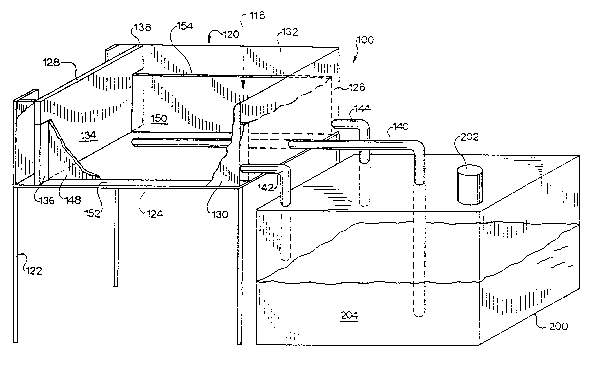
Referring now to Figure 1, horizontal
electroplating apparatus 100 is shown as including
coating tank 120 and reservoir tank 200 operably
connected to provide a flow of electrolyte 204 from
reservoir tank 200 to coating tank 120 and return. All
parts of the apparatus may be made of any suitable
material or materials of sufficient for the desired
purpose. The materials must be inert to the
, .
.
electrolyte 204 and strong enough to support the other
parts of the apparatuss 100.
Coating tank 120 is shown as positioned above
reservoir tank 200 to provide for gravity return of the
overflow coating solution or electrolyte 204 to the
reservoir tank 200. The coating tank 120, which is
generally in the shape of a hollow, topless rectangular
solid, is supported on four legs 122 which are secured
to the tank floor 124 for apparatus 100. Tank floor 124
provides for a base. The sides of coating tank 120
include a closed tank rear 126 and an open tank
front 128 oppositely disposed from the closed tank
rear 126. First tank side 130 is perpendicular to the
closed tank rear 126 and the open tank front 128 as is
second tank side 132. First tank side 130 and second
tank side 132 are oppositely disposed from each other
thereby forming a hollow rectangular area suitable for
coating.
A sliding door 134 fits into open tank front 138
and provides a liquid tight seal for a coating
chamber 118 within coating tank 120. The coating
chamber 118 within coating tank 120 is formed in a first
part by sliding door 134. Sliding door 134 fits into a
first sliding door slot 136 and in a second sliding door
slot 138 and forms a substantially liquid proof seal
with the printed circuit board 240.
The fluid inlet pipe 140 runs from that
reservoir tank 200 into the coating chamber 118. It is
pump 202 situated on reservoir tank 200 which forces the
electrolyte 204 through fluid inlet pipe 140 into the
coating chamber 118.
Coating chamber 118 is basically formed within
coating tank 120 by the board mounting assembly 146.
Board mounting assembly 146 includes a first support
wall 148 and a second support wall 150. First support
wall 148 is displaced from first tank side 130 as
desired. First support wall 148 is not as tall as
: ' , ~ ' ' ' ~ -
-15-
coating tank 120 is deep.
Second support wall 150 is oppositely disposed
from first support wall 148 and is displaced from but
adjacent to second tank side 132. Second support
wall 150 is similar in shape to first support wall 148.
Between first support wall 148 and first tank side 130
is created first overflow cavity 152. When coating
chamber 118 is full, the first overflow cavity 152 can
receive electrolyte 204 without displacing any of
electrolyte 204 from the coating tank 120 and permit the
electrolyte 204 to flow through first fluid return
pipe 142 back to reservoir tank 200.
In a like fashion second support wall 150
combines with second tank side 132 to form the second
overflow chamber 154. In this fashion, electrolyte 204
is received in second overflow chamber 154 and returned
to reservoir tank (storage chamber) 200 through second
fluid return pipe 144. Pump 202 is secured in standard
fashion to reservoir tank 200 and recycle~ the
electrolyte 204 to the coating chamber 118.
Referring now to Figure 1 and Figure 2, within
coating chamber 118 is first board clamp 156 and second
board clamp 158. First board clamp 156 appears as a
part of first support wall 148. Second board clamp 158
appears as a part of second support wall 150. Within
first board clamp 156 is a first board holder 160.
Likewise second board clamp 158 includes second board
holder 162. First board holder 160 and second board
holder 162 provide for a slot to hold the printed
circuit board 140 within the coating chamber 118.
Positioned within the coating chamber 118 but
below the first board holder 160 and second board
holder 162 is a lower anode 164. Above first board
holder 160 and second board holder 162 is upper
anode 166. Both the upper anode 166 and lower anode 164
are within the coating chamber 118 along with printed
circuit board 242.
-16-
The first board holder 160 and second board
holder 162 provide for the horizontal mounting of the
printed circuit board 242 substantially parallel to
lower anode 164 and upper anode 166. In this fashion,
by providing electrolytes through feed pipe 140, lower
anode 164, upper anode 166, and printed circuit
board 242 or printed circuit board assembly 240 may be
immersed in electrolyte 204. Printed circuit board
assembly 240 is a sandwich affair of at least two
printed circuit boards 242 interconnected by coating
through aperture 254 (shown in Figure 3). Printed
circuit board assembly 240 and printed circuit board 242
may both be coated by this invention and may be used as
interchangeable terms.
The lower anode 164 i9 connected to a lower
anode connector 168 which is in turn connected to a
potentiometer 176. Likewise the upper anode 166 is
electrically connected to upper anode connector 170
which is in turn connected to potentiometer 176 (shown
in Figure 7).
Mounted in first board holder 160 is first
cathode assembly 172. Mounted in second board
holder 162 is second cathode assembly 174. The anodes
and the cathodes combine to provide for electric current
to be applied to the printed circuit board 242 as the
electrolyte 204 is flowing therethrough to permit the
plating to take place. First cathode assembly 172 and
second cathode assembly 174 are grounded in any suitable
fashion. Wire grounding 178 may be used as ~hown with
first cathode assembly 172. Frame grounding 180 (shown
in Figure 6) by implanted bar 182 in second board
holder 162 may also be used.
The cathodes of fir~t cathode assembly 172 and
second cathode assembly 174 are more clearly shown in
Figure 2 as is the board holding assembly. It is clear
that the electrolyte fluid inlet pipe 140 is positioned
below the printed circuit board 242. Preferrably the
*9~
fluid inlet pipe is positioned below the lower
anode 164. When assembled, tank floor 124, lower
anode 164, upper anode 166 and printed circuit board 242
are substantially parallel to each other and ground
level and completely within coating chamber 118 so that
all of these elements may be immersed in
electrolyte 204. It is the horizontal aspect of this
plating that permits coating of the apertures in the
most efficient fashion.
Referring now to Figure 3, Figure 4, and
Figure 5, a sandwich with a printed circuit board
assembly 240 is depicted. Within the printed circuit
board assembly 240 are a plurality of printed circuit
boards 242. The circuits on printed circuit board 242
generally have a copper layer 246 applied first. As a
photoemulsion 248 on top of the copper layer 246 on the
printed circuit boards 242 substrate to provide for
making of the circuit. The photographic or
photoemulsion 248 is exposed to light. The exposed or
unexposed emulsion 248 can be washed away. The
remaining copper layer 246 can then be etched from the
board 242 to form the printed circuit. The
apertures 254 in the board 242 provide for the coating
and connecting of the various circuits. Nickel 250 or
other suitable conductive coating is applied first.
This coating is topped by a highly conductive noble
metal such as gold 252.
Figure 6 depicts the coating of the nickel or
similar metals with the appropriate anodes containing
the desired metals such as nickel to feed the solution.
Assuming for the sake of argument, that nickel is the
coating material, lower anode 164 and upper anode 166
(of Figure 2) are replaced with a lower inert screen 210
and and an upper inert screen 212 respectively.
Supported on each of lower inert screen 210 and and
upper inert screen 212 are nickel pieces 214. These
nickel pieces 214 dissolve in the electrolyte 204 and
- :
92
-18-
provides additional coating nickel.
Figure 7 depicts an inert anode assembly wherein
the plating for printed circuit board assembly 240 is
taken entirely from the electrolyte 204. The
composition of lower anode 164 and upper anode 166 is
basically an inert metal screen with a noble metal
coating. Typically, the noble metal preferred for
coating lower anode 16~ or upper anode 166, when noble
metal electroplating is desired, is platinum. The anode
in this case does not provide electroplating material.
Figure 8 is a side view of multiple plate
coating tank 300 as a modification of horizontal
electroplating apparatus 100 and is substantially
similar to Figure 2. Coating chamber 118 of Figure 2 i8
the same as multiple coating chamber 302 but for having
two units to hold two of printed circuit board
assembly 240 in a stacked horizontal arrangement. First
multiple board clamp 304 appears as a part of first
multiple support wall 306. Second board clamp 308
appears as a part of second multiple support wall 310.
Within first multiple board clamp 304 are two of first
board holder 160. Likewise second multiple board
clamp 308 includes two of second board holder 162.
Positioned within the multiple coating
chamber 302, below a lower of printed circuit board
assembly 240 is lower anode 164. Above both printed
circuit board assemblies 240 is upper anode 166.
Between the upper anode 166 and lower anode 164, and the
printed circuit boards 242 is middle anode 312 -- all of
these elements being within multiple coating chamber 302
and thus immersible in electrolyte 204. Thus, two of
printed circuit board 242 may be coated in one step.
Figure 9 is a side view of continuous coating
tank 400 as a modification of horizontal electroplating
apparatus 100 having a first coating tank 420 and a
second coating tank 422. Continuous coating tank 400
differs from coating tank 120 (shown in Figure 2) in
-19-
that there two ~f 31iding door 134 Yhown in Figure 2
oppo~itely disposed for a conveyor action o~ coating.
The continuous coating tank 400 may be as numerous as
desired as may the coating~ applled therein. Clearly
first coating tank 420 ~nd second coating tank 422 may
apply the ~ame or different coatings. The rinse
assembly 410 between each continuous coating tank 400 i9
optional and u~ed to clean the printed circuit board 242
iE desired. It i~ clear that thl~ proces~ and apparatus
may be modified to run on a continuous basis.
~rhe followinq example~ are intended to
illuHtrate without unduly limitin(1 the invention. All
part~ ani per~entageu are ,le~ined by w~lght oE the total
(0Il~ 9~tlon unlea9 olh~rwi~e ~peci~led.
Ixaml)le ~
A copp~ plated flberglaA~ board coat~d witll a
~llOLO~IllUI~lOn ifl ~xpo~ed to ~ negatlvo o~ c~rcult
d on th~ bodrd. The expoHed photo~mulsion i~
wl3hed off. Th~ board 1~ th~n s~cured in ~he app~r~tuu
~LI ~QpiCt~d ill Flgur~ 6. ~ nlckel coating ~olution
(comm~rcially available from ACR, Inc. of Waterbury,
Connectlcut, under the name #3~000X*) i8 flow~d thrl>ugh
th~ chamber and upwardly throuqh the board while
curr~nt of 10 ampA is flowed through the boar~. A
uniform coating of nickel i~ achieved, at about 0.000200
of an inch (or 0.00508 millimeter).
Example 2
The board of Example 1 then secured in the
apparatus as depicted in Figure 7. A gold coating
solution (commercially available from ACR, Inc. of
Waterbury,;Connectlcut~ under the name ACR 261) is
flowed through the chamber and upwardly through the
board while a current of 10 amp~ is flowed through the
board. A uniform coating of gold is achieved, at about
0.000051 of an inch ~or 0.00130 millimeter).
Example 3
A copper plated fibergla~s board coated with a
*trade-mark
. ..
92
-- ~o--
,, .
photoemulaion i~ expoaed to d net3ative of circuit
de~ire~ on the board. The expc;taad photoemul~ion i~
washed off. The bo~rd i~ then secured vertically in an
electroplating apparatus of prior art anc~ coated with
nick~l using thQ nlckel coating solution of Example
while n current of l~ amps i~ ~lowed through the boar~.
A non-uniform coating of nickel i9 achieved.
Connections botween variou~ p~rta of thq
apparatu~ disclo~ed her~in ar~t well-known in the art.
l~ydraulic connection~ and tank hosr~s are secured in any
~tnn~inrd non-l~akln~ fanhlon. tlouea fllter~ pump~ and
othor partA ~r~ mount~td d~ d~tnlrrtd unl~ a ~po~lflc
mOlJntl119 pl~c6t iU ~poci~l~t-J horeln.
Thlo ~pllc~tlon -- t~k-~n .1n ~ whol~ wlLh th~
I`t apocl~icntlorl cl~lm~ ~butr~ tnd rlr~wlnlu --
pr~vt~u ~uf~lclent Irl~ormqtlon ~or a per~on h~vln-3
~tr~in~ry nklll ln tho ~rt to pr~ctlce th~ lnv~rltlon
ttncloHo(J nn-t cl~lm~d h~ratin. Any ~neaauroa n~CoAaory t~
pr~ct~ thJn lnv~ntlon aro w~ll wlthln th~ ahlll ot o
~o p~r~orl hnvlng orilnary ~kJIl In Ihtn ~rt rt~or Ih.lt
r~ ha~ m~g* A ~Ar~lJ~ .~t~ y ~tL t~llQ lJl~cl-~tH~ u.
Hccauao o~ th~ l11nclGt~llr Ind ~ololy t~nllu~l- cL
Itlla dlnclo~urr~ modlEI(ItlonA r~ thl~ m thl)d ~nd
.ppned~u~ can bl~comQ cloar to ~ ptruoll h/lvtllll olltlln~y
~5 ~kill in thi~ pnrtlcullr nrL. ~U-tl rnodificltioll:i nrO
clearly covered by thls dlaclo~ur-.
What i~ clalmed and ~ought to b~ urotoct~-d tty
Lett~rs Patent i~: