Note: Descriptions are shown in the official language in which they were submitted.
2000~i83
TITLE OF THE INVENTION
Transmission Line Branching Device
BACKGROUND OF THE INVENTION
This invention relates to a branching device
interposed in a half duplex transmission line.
More specifically, the present invention relates to a
branching device which is used to connect branch lines
of communication module appliances disposed at
individual machining stations to a main transmission
line.
Conventionally, a communication system is known
wherein sequence controllers and computers disposed at
individual machining stations in a factory, are
connected to a main transmission line to effect mutual
communications between them. Robots, numerically
controlled machine and so forth disposed at the
individual machining stations are controlled by way of
the communication system.
In the communication system, branch lines of
individual communication module appliances are connected
to the main transmission line. Accordingly, when a
failure such as breaking of a wire, short-circuiting or
the like occurs at one of the branch lines to the
2(~00583
communication module appliances or at the main
transmission line, it is difficult to find o~lt the
location of the failure or to determine a manner of the
failure. When a failure of breaking of a wire occurs,
it is possible to separate the station in failure to
allow each of the other stations free from failure to
continue its processing by connecting the main
transmission line into a loop. However, when a failure
of short-circuiting occurs, communications between all
of the communication module appliances are disabled.
Therefore, in order to find out a location of a failure
of short-circuiting, it is necessary to devide the
transmission line in many sections and check them in an
order. However, this is a very difficult operation.
Accordingly, once the system fails, the entire
system must be stopped, and much time is required for
discovery of the failure and elimination of the trouble.
Besides, there is a possibility that, when one of
the communication module appliances connected to the
main transmission line by way of the branch lines is
damaged by an overvoltage or an overcurrent, such damage
may not be restricted to part of the system but may
reach the entire system.
Some of the inventors of the present invention have
2000583
proposed a multiplex communication system for a sequence
controller to solve such a problem. In the present
invention, moreover, reduction of time required for
elimination of a trouble upon failure of a system is
anticipated.
SUM~RY OF THE INVENTION
Accordingly, it is an object of the present
invention to attain rapid elimination of a trouble after a
communication system fails.
It is another object of the present invention to
provide a branching device which facilitates rapid
elimination of a trouble particularly against a failure of
short-circuiting of a transmission line.
It is a further object of the present invention to
provide a transmission line branching device wherein, when a
failure of breaking of a wire, short-circuiting or the like
occurs at one of branch lines of communication module
appliances or at an intermediate main transmission line,
elimination of the trouble can be carried out rapidly without
requiring much time for discovery of the location of the
failure or for determination of a manner of the failure, and
the failed
~- A 3
. .
28007-3
Z000583
station can be separated from the transmission line
without having an influence on any other communication
module appliance while processing can be continued at
any other station free from failure.
~ transmissi~n line branching device of the present
invention, having three terminals, may be interposed in
the half duplex transmission line and transmit an
electric signal received from an arbitrary one of three
terminals thereof through the other two terminals.
Since the terminals are coupled to each other by way of
photo-couplers, short-circuiting in a transmission
system connected to any one of the terminals does not
have an influence upon transmission systems connected to
the other terminals.
An electrical signal propagated over one of the
half duplex transmission lines connected to the three
terminals is received by a corresponding receiver by way
of a corresponding one of the terminals. The electrical
signal thus received is transmitted to drivers
corresponding to the other two terminals by way of the
photo-couplers. Thus, a signal propagated from an
arbitrary direction is branched in two directions for
further propagation in this manner. In this instance,
in order to prevent possible interference between
;~00Q1583
different signals, the transmission directions are
controlled in the fo]lowing manner.
The head of a data block of communication data
rec~ived hy each receiver is detected, and after sucl
detection of the head, a signal which specifies the
length of the data block (for example, a signal which
presents a high level while the data block is passing)
is generated. Then, after communication data are
received by way of an arbitrary one of the terminals and
a data block is detected, reception of communication
data from the other two terminals is inhibited while
transmission of the communication data from the other
two terminals is enabled.
Since the transmission lines of the three
directions of communication data are electrically
isolated from each other by means of the photo-couplers,
even when a failure of short-circuiting occurs at a main
transmission line or at a branch line or the like, the
failure can be regarded as an equivalent to breaking of
a wire. When the failure occurs at a branch line, the
branch line is automatically separated from the main
transmission line. On the other hand, when the failure
occurs at the main transmission line, restoration of
communications can be made by connecting the main
CA 02000~83 1998-01-22
transmisslon llne lnto a loop.
In accordance wlth the present lnventlon, there ls
provlded a transmlsslon line branching devlce adapted to be
lnterposed among three half duplex transmlssion lines for
~ sendlng out an electrlcal signal, whlch ls recelved at an
arbltrary one of three termlnals thereof lndlvldually
connected wlth sald half duplex transmlsslon llnes, through
the other two termlnals to the correspondlng two transmlssion
llnes connected therewlth, comprislng: three recelvers
lndividually provided for said termlnals and each adapted to
recelve, by way of a correspondlng one of sald termlnals, an
electrical slgnal propagated over a correspondlng one of sald
half duplex transmlsslon llnes; three drlvers lndlvldually
provlded for sald termlnals and each adapted to send out, by
way of a correspondlng one of sald termlnals, an electrlcal
slgnal to a correspondlng one of sald half duplex
transmlsslon llnes; flrst photo-couplers lndlvidually
connected wlth sald recelvers and each adapted to convert an
electrlcal slgnal recelved from a correspondlng one of sald
recelvers lnto an optlcal slgnal and convert the optlcal
slgnal agaln lnto an electrlcal slgnal; second photo-couplers
lndivldually connected wlth inputs of said drlvers and each
adapted to dellver an electrical slgnal to a correspondlng
one of sald drivers; a distributing circuit for connecting an
output of one of sald flrst photo-couplers correspondlng to
an arbitrary one of said terminals wlth those of sald second
photo-couplers correspondlng to the other two termlnals;
three data block detectlng means individually provided for
28007-3
CA 02000~83 1998-01-22
said recelvers and each adapted to detect the head of a data
block of communlcatlon data recelved by way of a
correspondlng one of sald recelvers and generate, after such
detectlon of the head, a slgnal whlch speclfles the length of
the data block; and a data receptiontsending changing over
means responsive to an output slgnal of an arbltrary one of
sald data block detectlng means, when a data block of
communlcatlon data ls detected by the arbltrary data block
detectlng means, for inhiblting receptlon of communication
data by way of the other two termlnals and enabling sendlng
of the communication data from the other two terminals.
~RIEF DESCRIPTION OF THE DRAWINGS
Flg. 1 ls a block dlagram showlng a transmlsslon
llne branchlng devlce accordlng to a preferred embodlment of
the present lnventlon;
Flg. 2 ls a dlagram showlng a data block of
communlcatlon data to be transmltted by way of the
transmlsslon line ~ranching device of Fig. l;
Flg. 3 ls a block dlagram showlng an entlre
communlcatlon transmlsslon system lncludlng the transmlsslon
llne branchlng devlce of Flg. l;
Flg. 4 ls a detalled clrcult dlagram showlng a
transmlsslon devlce shown ln Flg. l;
Flg. 5 ls a block dlagram showlng constructlon of a
transmlsslon llne branchlng devlce accordlng to another
preferred embodiment of the present invention;
Flg. 6 is a block diagram showlng constructlon of a
transmission line branching devlce according to a further
6a
28007-3
CA 02000~83 1998-01-22
preferred embodlment of the present lnventlon;
Flg. 7 ls a detalled clrcult diagram showing a
transmlsslon devlce shown ln Flg. 6; and
Flg. 8 is a block diagram showing construction of a
transmlsslon line branchlng devlce according to a still
6b
28007~3
200(~583
further preferred embodiment of the present invention.
DESCRIPTION OF THE INVENTION
In the following, the embodiment of the present
invention will be described with reference to the
drawings.
At first, construction of a transmission system
including a transmission line branching device
of the present invention will be described with
reference to Fig. 3.
A transmission line branching device 1 according to
the present invention may be disposed at a junction at
which a branch line B of each communication module
appliance S is connected to a main transmission line M.
Referring also to Fig. 1, communication data
input/output connecting terminals PC, IN and OUT of
transmission devices 1Oa, 1Ob and 10c of such
transmission line branching devices 1, the branch lines
B of the individual communication module appliances S
and the main transmission line M are interconnected in
such a manner as shown in Figs. 1 and 3.
Referring to Fig. 1, the transmission line
branching device 1 shown includes the three transmission
devices 1Oa, 1Ob and 10c, each having such communication
2000583
data input/output connecting terminals PC, IN and OUT.
The transmission device 1Oa, 1Ob and 10c are connected
to each other by way of a distributing circuit 20. The
distributing circuit 20 is composed of three OR getes
20a, 20b and 20c.
The transmission devices 1Oa, 1Ob and 10c have a
similar construction to each other, and the transmission
device 1Oa will be described as a representative in the
following.
The transmission device 1Oa includes a receiver 11a
to which a photo-coupler 12a and a first data block
detecting circuit 15a are connected. The first data
block detecting circuit 1Sa detects a start bit in a
data block of an output signal of the receiver 11a and
generates a maintaining signal to maintain the receiver
11a in a signal passage enabling condition for a
predetermined period of time during which at least the
data block can be transmitted (time length of the data
block).
Details of the first data block detecting circuit
1Sa are shown in Fig. 4. Referring to Fig. 4, an output
of an invertor 151 is coupled to a ~type flip-flop
circuit 152, and a ~ terminal output of the ~type flip-
flop circuit 152 is coupled to a succeeding D-type flip-
2000583
flop circuit 153. A Q-terminal output of the D-type
flip-flop circuit 153 and the ~termina] output of the
y~c Lli~Llo~ ~ircui(; 15;~ arc c~)upl~ all ANL) y~c
154. An output of the AND gate 154 is coupled to an RS-
type flip-flop circuit 155 and a timer 157. A timing
for latching at the D-type flip-flop circuits 152 and
153 is provided by a clock signal given from a clock
generator 156. Meanwhile, the timer 157 starts its
counting operation after the output of the AND gate 154
changes from a low level (hereinafter referred to as L
level) to a high level (hereinafter referred to as H
level), and after a predetermined interval of time
elapses, the timer 157 resets the RS-type flip-flop
circuit 155. An output of the RS-type flip-flop 155 is
coupled to another AND gate 171 which constitutes a
transmission direction changing over signal generating
circuit 17a.
Meanwhile, an output of the photo-coupler 12a is
coupled to the OR gates 20b and 20c as shown in Fig. 1.
On the other hand, communication data from the
other two terminals which are transmitted by way of the
OR gate 20a from the other transmission devices 1Ob and
1 0c are coupled to a driver 1 4a by way of a photo-
coupler 13a and then sent out from the connecting
~058;3
terminal PC by the driver 14a.
Further, a second data block detecting circuit 16a
is provided to detect a start bit in a data block of an
output signal received from the photo-coupler 13a and
generate a maintaining signal to maintain the driver 14a
in a signal transmission enabling condition for a
predetermined period of time during which at least the
data block can be transmitted.
Details of the second data block detecting circuit
16a are also shown in Fig. 4. As seen in Fig. 4, the
second data block detecting circuit 16a has a similar
construction to that of the first data block detecting
circuit 15a but is different in that an invertor 161 is
connected to receive an output signal of the photo-
coupler 13a.
The transmission direction changing over signal
generating circuit 17a is connected to receive signals
from the first and second data block detecting circuits
15a and 16a and deliver a control signal in accordance
with a predetermined logic to a control terminal of the
driver 14a and an invertor 18a. An output of the
invertor 18a is coupled to a control terminal of the
receiver 1la. In response to a level of such control
signal from the transmission direction changing over
1 0
ZQ~OS83
signal generating circuit 17a, either the receiver 11a
is put into a signal passage enabling condition and the
driver 14a is put into a signal passage disabling
condition or on the contrary the receiver 11a is put
into a signal passage disabling condition and the driver
14a is put into a signal passage enabling condition.
The output of the receiver 11a normally presents,
in a no-signal condition, thell level as shown in
Fig. 2. ~ dat.~ block cilangcs rrom tllc ll lcvcl to tllc L
level and has, after then, a start bit consisting of two
bits of the L level. The data block normally terminates
with a stop bit of the H level.
The time T from the beginning of the start bit to
the stop bit is a transmission duration of a data block
(data length in time). The level maintaining periods of
time of maintaining signals given from the first
data block detecting circuit 15a and the second data
block detecting circuit 16a are a little longer than the
duration T. The periods of time are set by means of
built-in timers.
Subsequently, operation of the transmission line
branching device will be described.
Since the transmission devices 1Oa, 1Ob and 10c
operate in a similar manner to each other, description
2000583
will be given of operation of the transmission device
1Oa as a representative
After the power is made available to the
transmission line branching device 1, the transmission
device 1Oa stands by in a condition wherein it can
accept data from the connecting terminal PC. Initial
states of the RS-type flip-flop circuits 155 and 165 are
reset states. Accordingly, the Q-terminal output of the
RS type flip-flop circuit 165 presents the L level, and
consequently the output of the AND gate 171 presents the
L level. As a result, the driver 14a remains in an
inoperative condition. On the other hand, since the
output signal of the invertor 18a presents the H level,
the receiver 11a is in an operative condition.
Accordingly, presence or absence of an electrical signal
transmitted by way of the connecting terminal PC can be
monitored by the first data block detecting circuit 15a.
Meanwhile, presence or absence of an electrical signal
received by way of the other two terminals and
transmitted to the transmission device 1Oa by way of the
photo-coupler 13a is normally monitored by the second
data block detecting circuit 16a.
Subsequently, in case an electrical signal is
received by way of the connecting terminal PC, such an
ZC~0583
electrical signal as shown in Fig. 2 is transmitted to
the D-type flip-flop circuit 152 by way of the invertor
151 because the receiver 11a remains in an operative
condition. The requirement with which the output of the
AND gate 154 is changed to the H level lS that the ~
terminal output of the D-type flip-flop circuit 152 and
the Q-terminal output of the D-type flip-flop circuit
153 both present the H level. Since the D-type flip-
flop circuits 152 and 153 form a 2-position shift
register, if the output signal level of the receiver 11a
changes from the H level to the L level, then the
requirement is satisfied. In particular, when a start
bit is detected, the output of the AND gate 154 is
changed from the L level to the H level. Consequently,
the timer 157 starts its counting operation while the
RS-type flip-flop 155 is set. Accordingly, the Q-
terminal output of the RS-type flip-flop circuit 155 is
changed from the H level to the L level, and
consequently the output of the AND gate 171 maintains
the L level irrespective of an output level of the
second data block detecting circuit 16a.
The timer 157 resets the RS-type flip-flop circuit
155 after the transmission period T of the data block
elapses. Consequently, the output signal from the Q-
2~0~583
terminal of the RS-type flip-flop 155 is changed back to
the H level of the initial state. The H level of the Q-
terminal output of the RS-type flip-flop circuit 155
makes an enabling signal for enabling the change of the
transmission direction in accordance with the Q-terminal
output of the RS-type flip-flop circuit 165. To the
contrary, the L level of the Q-terminal output of the
RS-type flip-flop circuit 155 makes a maintaining signal
for maintaining the initial transmission direction in
which the receiver 11a is active. Accordingly, at least
during the transmission time T of the data block, the
receiver 11a maintains an operative condition while the
driver 14a maintains an inoperative condition, and
consequently the output signal of the receiver 11a is
transmitted to the photo-coupler 12a.
Before the transmission duration T of a data block
elapses, there is no communication data to be received
via the photo-coupler 13a from other two terminals IN,
OUT as hereinafter described.
However, if communication data should be received via
the photo-coupler 13a, then the second data block
detecting circuit 16a will detect a start bit.
Consequently, the maintaining signal to be given
from the circuit 16a is changed from the L level to the
14
Z~)~0583
H level, but since the Q-terminal output of the RS-type
flip-flop circuit 155 remains at the L level, the output
signal of the transmission direction changing over
signal generating circuit 17a maintains the L level.
Accordingly, there is no change from the operative
condition of the receiver 11a and the inoperative
condition of the driver 14a. Due to such control,
reception takes precedence over sendir-g to prevent
electrical signals from interfering with each other on
the half duplex transmission lines.
Subsequently, an electrical signal received by way
of the connecting terminal PC is transmitted, by way of
the photo-coupler 12a and the OR gates 20b and 20c, to
the second data block detecting circuits 16b and 16c of
the other transmission devices 1Ob and 10c,
respectively.
Operation of the transmission devices 1Ob and 10c
then will be described as a representative in connection
with the transmission device 1Ob. Referring to Fig. 4
which also shows details of the transmission device 1Ob,
it is assumed that there is no electrical signal
received via the connecting terminal IN from the branch
line B then. In this instance, the Q-terminal output of
the RS-type flip-flop circuit 155, that is, the output
~000583
of the first data block detecting circuit 15b, is at the
H level. Meanwhile, the Q-terminal output of the RS-
type flip-flop circuit 165, that is, the output of the
second data block detecting circuit 16b, normal ly
presents the L level. Then, when a data signal is
delivered from the photo-coupler 13b, transition of the
signal level from the H level to the L level is detected
by the D-type flip-flop circuits 162 and 163.
Consequel1tly, the output of tlle I~ND gate 1G4 is char-ged
from the L level to the H level to set the RS-type f lip-
flop circuit 165. As a result, the output of the AND
gate 171 is also changed from the L level to the H
level because the Q-terminal output of the RS-type
flip-flop circuit 155 of the first data block detecting
circuit 1 5b is the H level, by which the receiver 11 b is
put into an inoperative condition while the driver 14b
is put into an operative condition. Such conditions are
maintained until the transmission duration T of a data
block is counted up by the timer 167 as described
hereinabove. Accordingly, during the period of time T,
data received from the connecting terminal PC by way of
the photo-coupler 12a, OR gate 20b and photo-coupler 13b
are transmitted from the connecting terminal IN to the
branch line B by way of the driver 14b. In the
16
Z0(~(:t583
meantime, reception of communication data from the
connecting terminal IN is inhibited on the contrary.
~ fter the period of time T elapses, the timer 167
resets the RS-type flip-flop circuit 165 to change the
output of the latter from the H level to the L level.
Consequently, the output of the AND gate 171 is changed
into the L level to restore the transmission direction
to the initial in which reception by the receiver 11b is
enabled.
Also the transmission device 10c which is connected
to the connecting terminal OUT operates in a similar
manner to the transmission device 1Ob. Accordingly, an
electrical signal received from the connecting terminal
PC is transmitted from the connecting terminals IN and
OUT.
Similarly, an electrical signal received by way of
the connecting terminal IN is delivered from the
connecting terminals PC and OUT. Similarly, an
electrical signal received by way of the connecting
terminal OUT is delivered by way of the connecting
terminals PC and IN.
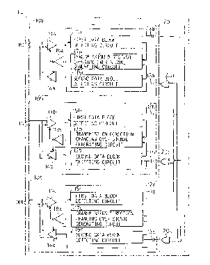
Subsequently, another embodiment of the present
invention will be described with reference to Fig. 5.
Here, elements having like functions to those of Fig. 1
2~583
are denoted by like reference characters, and
description will be given only of differences of the
transmission line branching device of the present
embodiment from those of the transmisslon line branching
device of the preceding embodiment.
For example, communication data received by way of
the connecting terminal PC side of a transmission device
40a of a transmission line branching device 1 are
transmitted to a data block detecting circuit 41a by way
of a receiver 11a. When the data block detecting
circuit 41a, detects a start bit of a data block of the
communication data received, the output signal thereof
is changed from the L level to the H level. In
particular, while the data block detecting circuit 41a
has a similar construction to that of the data block
detecting circuit 15a of the first embodiment, here the
Q-terminal output of the RS-type flip-flop circuit 155
makes an output signal of the data block detecting
circuit 41a the H level of which means the duration T
for the received data to be transmitted. The output
signal of the H level given from the circuit 41a is
transmitted by way of OR gates 42b and 42c of the other
transmission devices 40b and 40c to put drivers 14b and
14c into an operative condition, respectively.
200058;~
Meanwhile, since the output signals of invertors 18b and
18c are changed from the H level to the L level when the
output signal of the data block detecting circuit 41a
changes from the L level to the H level, receivers 11b
and 1lc are put into an inoperative condition thereby.
Simultaneously, the communication data transmitted by
way of the receiver 11a is transmitted to the drivers
14b and 14c by way of a photo-coupler 12, OR gates 20b
and 20c of a distributing circuit 20 and photo-couplers
13b and 13c. Since the drivers 14b and 14c remain in an
operative condition and the receivers 11b and 11c remain
in an inoperative condition then, the communication data
are sent from the connecting terminals IN and OUT by way
of the respective transmission devices 40b and 40c to
the branch line B and the main transmission line M. In
the meantime, reception of communication data by way of
the connecting terminals IN and OUT is inhibited. Then,
when the data block detecting circuit 41a of the
transmission device 40a detects a stop bit of a data
block of the communication data received, the output
signal thereof is changed from the H level to the L
level. The output signal then is transmitted by way of
the OR gates 42b and 42c of the other transmission
devices 40b and 40c to put the drivers 1 4b and 1 4c into
1 9
20C~0583
an inoperative condition. Meanwhile, since the output
signals of the invertors 18b and 18c are changed to the
~ level, the receivers 11b and 11c are changed back into
an operative condition of the initial state. It is to
be noted that such operation described above similarly
applies where communication data are received from the
connecting terminal IN or OUT of the transmission device
40b or 40c.
Subsequently, a further embodiment of the present
invention will be described with reference to Fig. 6.
Also, elements having like functions to those of Fig. 1
are denoted by like reference characters, and
description will be given only of differences of the
transmission line branching device of the present
elllbodiment from tllose of tl1e translllissiol1 line brancl~ing
device of the preceding first embodiment.
In the initial state, Q-terminal outputs and Q-
terminal outputs of data block detecting circuits 51a,
51b and 51c are the L level and the H level,
respectively. Accordingly, outputs of AND gates 53a,
53b and 53c are the L level to cut off analog gates 52a,
52b and 52c. Communication data received from the
connecting terminal PC side of a transmission device 50a
of a transmission line branching device 1 are
-
i0583
transmitted to the data block detecting circuit 51a by
way of a receiver 1la. Detailed construction of the
data block detecting circuit 51a is shown in Fig. 7.
The construction is similar to that of the first data
block detecting circuit 15a of the first embodiment
described hereinabove. Referring also to Fig. 7, a Q-
terminal output of an RS flip-flop 155 is coupled to an
AND gate 53a. The outputs of Q-terminals of RS flip-
flop circuits 155 of the other data block detecting
circuits 51b and 51c corresponding to the other connecting
terminals of the transmission line branching device are
coupled also to the other two input terminals of the AND
gate 53a. Meanwhile, a Q-terminal output of the RS-type
flip-flop circuit 155 of the data block detecting
circuit 51 a is coupled to AND gates 53b and 53c of the
transmission device 50b and 50c corresponding to the
other connecting terminals of the transmission line
branching device. The outputs of the AND gates 53a, 53b
and 53c are coupled to control terminals of the analog
gates 52a, 52b and 52c, respectively.
Subsequently, operation of the transmission line
branching device will be described.
When the data block detecting circuit 51a detects
reception of communication data by way of the connecting
Z~0583
terminal PC, the Q-terminal output of the data block
detecting circuit 51a (Q-terminal output of the RS-type
flip-flop circuit 155) presents the H level for a period
of time of passage of the data block. On the contrary,
the Q-terminal output of the data block detecting
circuit 51a (Q-terminal output of the RS-type flip-flop
circuit 155) presents the L level for the period of time
of passage of the data block. Consequently, the output
of that one of the AND gates 53a, 53b and 53c which
corresponds to one of the three connecting terminals PC,
IN and OUT of the transmission line branching device at
which the communication data are received in the first
place presents the H level while the output signals of
the AND gates 53 corresponding to the other two
connecting terminals present the L level for the period
of time of passage of the communication data.
Accordingly, only one of the analog gates 52a, 52b and
52c which corresponds to the connecting terminal at
which communication data are received in the first place
is put into a signal passage enabling condition. The
following description will proceed on the assumption
that the analog gate which is put into a signal passage
enabling condition in the first place is the analog gate
52a corresponding to the connecting terminal PC.
~00(1 58~
Thus, a signal received by way of the connecting
terminal PC is transmitted by way of the receiver 11a,
analog gate 52a, photo-coupler 12a, OR gates 20b and 20c
and photo-couplers 13b and 13c to the drivers 14b and
14c and sent out by way of the connecting terminals IN
and OUT to the branch line B and the main transmission
line M, respectively.
Meanwhile, since the Q-terminal output of the data
block detecting circuit 51a presents the L level while
the data block continues to be received, the outputs of
the AND gates 53b and 53c present the L level.
Consequently, the analog gates 52b and 52c maintain a
signal passage disabling condition. Accordingly, the
outputs of the receiver 11b and the receiver 11c are not
propagated to the other connecting terminals.
Then, when the reception of the data block of the
communication data has been completed, the Q-terminal
output signal thereof is changed from the H level to the
L level. Then, since the output signal is transmitted
to the AND gate 53a, the output signal of the AND gate
53a is changed to the L level. Consequently, the analog
gate 52a is put into a signal passage disabling
condition and is thus disconnected from the other
connecting terminals.
0583
Meanwhile, the Q-terminal output of the data block
detecting circuit 51a is changed to the H level to be
entered into the AND gates 53b and 53c. Accordingly,
the outputs of the AND gates 53b and 53c are controlled
by the levels of the Q-terminal outputs of the data
block detecting circuits 51b and 51c, respectively.
Therefore, if the data block detecting circuit 51b or
51c detects a data block, then the analog gate 52b or
52c will be put into a signal passage enabling condition
at any time.
It is to be noted that such operation as described
above similarly applied where communication data are
received at the connecting terminal IN or OUT side of
the transmission device 50b or 50c.
As apparent from the foregoing description of the
embodiments, since the transmission line branching
devices 1 are electrically isolated from one another,
even if a failure of short-circuiting occurs at a
communication module appliance S or a branch line B,
processing can be continued at any other station free
from failure.
Further, in case a failure of breaking of a wire or
short-circuiting takes place at the main transmission
line M, a loop line should be provided such that, for
24
Z000583
example, it may connect the left and right opposite
directions of the main communication line M as indicated
by a broken line in Fig. 3. Then, a normally-open
switch SW1 may be provided in tl1e loop line. 'l'hus, if
the switch SW1 is operated, then processing can be
continued at any station. And it is possible to repair
the failure of breaking of a wire or short-circuiting or
the like of the main transmission line M with keeping
the normal communications.
Here, if data transmission becomes impossible at
any transmission line branching device 1 due to a
failure of or interruption of the power supply to the
transmission line branching device 1, communications
will be come impossible through the main transmission
line M or a branch line B of a communication module
appliance S and the equipment will be stopped. Even if
there is no such failure at the main transmission line M
or at any branch line B, there is a possibility that a
communication disabling condition may be caused by a
trouble at a transmission line branching device 1
itself. As a countermeasure, as shown Fig.8, bypass
transmission lines BT1 and BT2, which bypass among the
PC terminal, the OUT and the IN, may be provided for
each transmission line branching device 1, and
~V00583
mechanical switches SW2, SW3 and SW4 may be
individually disposed in such bypass transmission lines
BT1 and BT2. With the construction, if a transmission
line branching device 1 is put into a communication
disabling condition, then the transmission lines can be
l~ssllred temporarily and the relieL can be ma~e by
suitably operating the corresponding mechanical
bypassing switch SW2, SW3 or SW4. Thus, the time
required for an interval of time until restoration after
a communication disabling condition can be reduced.
26