Note: Descriptions are shown in the official language in which they were submitted.
20(~0597
OPTICAL RECORDING ELEMENT
FIELD OF THE IN~ENTION
The present invention relates to an optical recording
element for use in optically recording, erasing and playing
back information such as optical disks optical memory
cards and the like.
BACKGROUND OF THE IN~ENTION
Whilst there has been an increasing need for high
density memory systems capable of storing a large amount of
information and being accessed at a high speed, optical
recording elements capable of optically recording, erasing
and playing back information begin to attract attention.
Research and development especially aimed at improving DRAW
(Direct Read After Write) type optical disks, rewritable
optical disks and portable memory cards are expedited in
,_ 2~0Qss7
order to find wide application for the optical recording
elements.
Conventionally, a multiple-layer construction having
anti-reflection properties is widely employed in such
optical recording elements. As the optical recording
element of multiple-layer construction, there are known
i) optical recording elements comprising a recording medium
20 formed on one face of a transparent substrate 14, the
recording medium 20 including a recording layer 11,
transparent dielectric layer 12 and reflective film layer 13
(see Fig. 5(a)); (ii ) optical recording elements
comprising a recording medium 21 formed on one face of the
transparent substrate 14, the recording medium 21 including
two transparent dielectric layers 15 and 16, and the
recording layer 11 (see Fig. 5(b));and (iii) optical
recording elements comprising a recording medium 22 formed
on one face of the transparent substrate 14, the recording
medium 22 including two transparent dielectric layers 17 and
18, the recording layer 11, and the reflective film layer
13 (see Fig. 5(c)). These types of optical recording
elements have anti-reflection properties exhibited by the
interference effect of the transparent dielectric layers 12,
15, 16, 17 and 18 respectively.
In DRAW type optical recording elements, e.g.
punching type optical recording elements, the anti-
Z(~00sg7
reflection properties achieved by the multiple-layer
construction is essential for enhancing the contrast in the
reproduced information and obtaining high recording
sensitivity. Also, the above anti-reflection properties
are required in a magneto-optical recording element which is
widely known as a typical rewritable optical recording
element, in order to improve the playback performance by
enhancing the magneto-optical effects.
The aforesaid transparent substrate 14 is made of a
plastic such as polycarbonate resin, glass or the like. In
particular, it is possible to produce large quantities of
the substrates 14 made of a plastic at low cost by
injection molding or similar methods, and therefore such
substrates 14 are widely used. The recording layer 11 is
comprised of, for example, an amorphous rare earth-
transition metal thin film such as GdTbFe which is suitable
for magneto-optical recording.
Although the recording and playback performances of
the optical recording elements can be improved by the
conventional constructions, the amount of reflected light
from the recording layer 11 is inevitably decreased since
it is required to effectively cause the interference of
light at the abovementioned transparent dielectric layers
12, 15, 16, 17 and 18. Therefore, the optical recording
element having any of the above çonstructions has a dark
Z~)0~597
tone appearance, and shows up badly in comparison with
disks in which a material having metalic luster is used for
obtaining a high reflective factor such as compact disks and
video disks for playback use only; and magnetic cards
having a colorful design provided thereon such as cash
cards, credit cards and various prepaid cards.
The transparent substrate 14 composing the
conventional optical recording element tends to generate a
static charge, as apparent from the fact that the optical
recording element having the transparent substrate 14 of
polycarbonate resin shows a specific resistance of
approximately 1 X lOl~ Q cm on the surface thereof.
Since the surface of the transparent substrate 14 easily
gets dust because of the static charge, noise is generated
deteriorating the reliability of the optical recording
element.
SUMMARY OF THE INVENTION
It is an object of the present invention to provide
an optical recording element in which a reflective material
is used for reflecting lights having wavelengths in a
specified visible region of the spectrum, in order to make
the appearance of the optical recording element colorful.
It is another object of the present invention to
provide an optical recording element having improved
2(~00597
-
reliability with the surface which is not hardened even if
it comprises a transparent substrate made of a resin
material.
It is still another object of the present invention
to provide an optical recording element capable of
eliminating a static charge generated on the surface thereof
in order to prevent the adhesion of dust to the surface,
thereby increasing the reliability of the optical recording
element.
In order to achieve the above objects, an optical
recording element according to the present invention is
characterized in comprising: (i ) a transparent substrate
through which light passes; ~ii) a recording medium formed
on one face of the transparent substrate; and (~i) an
optical thin film composed of at least one layer, formed on
the other face of the transparent substrate so as to
transmit light beams used for recording, erasing and
playback, and reflect lights which have wavelengths
different from the wavelength of the above light beams and
are within a specified visible region of the spectrum. With
the above arrangement, lights having wavelengths in a
specified visible region of the spectrum are reflected at
the surface of the optical recordin~ element so that the
surface appears to be colored according to the wavelengths
of the reflected lights, and the disadvantage of a dark
200Q597
-
appearance can be thus overcome. On the other hand, light
beams used for the recording, erasing and playback of
information pass through the optical recording element, and
therefore there is no fear of damaging the functions of
recording, erasing and playback.
In order to achieve the above obiects, another
optical recording element according to the present invention
is characterized in comprising~ a transparent low-
resistance substrate having a specific resistance at the
surface thereof in the range from more than OQ cm to lX
10~Q cm; (ii~ a recording medium formed on one face of
the transparent low-resistance substrate, the face being
opposite to the side on which a light beam is incident; and
(iii) a protective layer formed on one face of the recording
medium, the face being opposite to the side at which the
transparent low-resistance substrate is formed.
Having a low specific resistance, i.e., lX 106Q cm
or less, the transparent low-resistance substrate in the
above arrangement is electrically conductive. More
specifically, when a static charge is generated on the
optical recording element, the transparent low-resistance
substrate can transmit the static charge outward thereby to
prevent the accumulation of static charges and the adhesion
of dust to the surface of the transparent low-resistance
substrate. Consequently, noise can be reduced.
2~)00597
This specification also discloses the manufacturing
method of the optical recording element having a low
specific resistance at the surface thereof.
The above and other objects of the present invention
will become more apparent from the following description
when taken in conjunction with the accompanying drawings.
BRIEF DESCRIPTION OF THE DRAWINGS
Figs. 1 to 3 respectively show one embodiment of the
present invention.
Fig. 1 is a sectional view of the essential parts of
an optical recording element according to the present
invention.
Fig. 2 is a graph showing the dependence of the
reflectivity on the wavelength at the optical recording
element in the respective cases the optical recording
element has a transparent dielectric thin film laminated
layer of bi-layer construction and it has a transparent
dielectric thin film laminated layer of quadri-layer
construction.
Fig. 3 is a graph showing the dependence of the
reflectivity on the wavelength at the surface of the
optical recording element having a transparent dielectric
thin film laminated layer of the quadri-layer construction
when the only thickness of a low refractive index
2~0~597
dielectric thin film is changed more or less from the value
of the thickness thereof obtained by the equation (1).
Fig. 4 is a vertical sectional view showing the
structure of an optical recording element according to
another embodiment, which has a low specific resistance.
Figs. 5(a) to (c) are sectional views respectively
showing the multiple-layer construction of a conventional
optical recording element.
DESCRIPTION OF THE EMBQDIMENTS
Referring to Figs. 1 to 3, one embodiment of the
present invention will be hereinafter described in detail.
The optical recording element of the present
invention, as shown in Fig. 1, comprises a transparent
substrate 1 through which light beams utilized for the
recording, erasing, playback of information pass; recording
medium 2 formed on one face of the transparent substrate 1;
and transparent dielectric thin film laminated layer 3
formed on the other face of the transparent substrate 1.
Like conventional optical recording elements, the recording
medium 2 has a construction for anti-reflection, in which
transparent dielectric layers, a reflective film layer and
a recording layer are formed in combination.
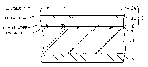
The transparent dielectric thin film laminated layer
3 includes high refractive index dielectric thin films 3a
2~0~)597
which are optical thin films having a refractive index
higher than that of the transparent substrate 1, and low
refractive index dielectric thin films 3b having a
refractive index lower than that of the transparent
substrate 1. These high refractive index dielectric thin
films 3a and low refractive index dielectric thin films 3b
are alternately laminated forming N layers, such that the
first layer, as viewed from the side on which light beams
used for the recording, erasing and playback are incident,
is the high refractive index dielectric thin film 3a.
Accordingly, the high refractive index dielectric thin film
3a is formed at the odd layers and the low refractive index
dielectric thin film 3b at the even layers. The thicknesses
of the high refractive index dielectric thin film 3a and
the low refractive index dielectric thin film 3b are
respectively given by:
n k d k = m (~ = 1, 2, 3 ~ -- (1)
where
n~ : the refractive index of the k-th transparent
dielectric thin film as counted from the side on
which a light beam is incident.
2~0597
dk : the thickness of the k-th transparent dielectric
thin film.
A : the wavelength of light beams used for recording,
erasing and playing back information.
With the above arrangement, due to the interference
effect of the multiple-layers, the reflectivity of the
optical recording element of multiple-layer construction is
equivalent to that of the optical recording element wherein
neither the high refractive index dielectric thin film 3a
nor low refractive index dielectric thin film 3b are
provided. The reflectivity for the incident light beam of
the wavelength~ is the minimum value. In other words, the
amount of reflected light becomes large when light having
other wavelengths than the above wavelength A is incident
on the optical recording element, and therefore the optical
recording element has colors corresponding to the
wavelengths of the reflected light.
I~ore concretely, when employing ZnS (the refractive
index n = 2.39) as the high refractive index dielectric
thin film 3a; ~gFz (the refractive index n= 1.39) as the
low refractive index dielectric thin film 3b; polycarbonate
(the refractive index n = 1.585) as the transparent
substrate 1, and setting the wavelength A of the light
beams used for recording, erasin~ and playback to 780 nm,
- 1 0 -
2000597
-
the thicknesses of the ZnS layer and MgF2 layer are
respectively obtained using the above equation (1). The
thickness tzns of the ZnS layer and the thickness t~gF2
of the MgF2 layer are approximately 163 nm and 281 nm
respectively. Under the above condition, the dependence of
the reflectivity on the wavelength at the surface of the
optical recording element is observed in the respective
cases that the transparent dielectric thin film laminated
layer 3 is composed of two layers ~i.e. in the case of N=2
in Fig. 1) and composed of four layers (i.e. in the case of
N =4 in Fig. 1). As shown in Fig. 2, in both cases, the
reflectivity is the minimum value Ro at the wavelength of
780 nm, and is high at the wavelength which is in the
vicinity of 520 nm (the reflectivity of the optical
recording element having no transparent dielectric thin film
is also the value Ro at the wavelength of 780 nm). Hence,
the light beams used for recording, erasing and playback
pass through the transparent substrate 1 without being
reflected so as to reach the recording film, while lights
(in this case, the lights whose wavelength is in the
vicinity of 520 nm) having other wavelengths than that of
the above light beams do not pass through the transparent
substrate 1 but are reflected thereat. As a result, an
optical recording element whose appearance is in yellow
tone can be obtained without damaging the recording,
XC)~597
erasing and playback functions of the optical recording
element. It often occurs that the surface of the
transparent substrate 1 is hardened by incident light beams,
when the transparent substrate 1 is of a resin material,
but such a drawback can be avoided in this embodiment
wherein an inorganic transparent dielectric thin film is
laminated on the surface of the transparent substrate 1.
When the thickness of the MgF2 layer serving as the
low refractive index dielectric thin film 3b more or less
differs from the value obtained by the foregoing equation
(1) (e.g. t~gF2 = 100 nm) and the transparent dielectric
thin film laminated layer 3 is of quadari-layer
construction (i.e. in the case of N = 4 in Fig. 1), the
dependence of the reflectivity on the wavelength at the
surface of the optical recording element is observed. As
shown in Fig. 3, not only is the wavelength region at which
the reflectivity of the optical recording element is high
wider compared with that in the first example shown in Fig.
2, but the reflectivity at the wavelength of 780 nm is lower
than the minimum value Ro. Therefore, the adverse
influence of light reflected at the surface of the optical
recording element in the course of recording, erasing or
playback operation can be reduced.
In the above examples, transparent dielectric thin
films which are optical thin films are laminated to form a
- 1 2 -
2000597
-
multiple-layer construction, whereby the light beams used
for recording, erasing and playback pass therethrough due
to the interference effect, while lights having wavelengths
within a specified visible region of the spectrum,
different from the wavelength of the above light beams are
reflected thereat. In lieu of the aforesaid transparent
dielectric thin film of multiple-layer construction, a
single optical thin film of mono-layer construction may be
employed. Also, it is to be understood that the transparent
dielectric thin film laminated layer 3 is not limited only
to the alternate layers of ZnS and MgF 2 ~ but other materials
may be employed in combination selecting from materials
such as SbzS3~ TiO2, CdS, CeO2, PbCQ z, WO3, SiO, AQ 203,
SiOz, CaF2, LiF, NaF, AQ N, SiN, etc. so as to satisfy the
aforementioned relation between two materials regarding the
refractive index. Further, in the foregoing embodiment, the
transparent substrate 1 is provided with the transparent
dielectric thin film laminated layer 3 at the surface
opposite to the surface on which the recording medium 2 is
formed, but it also may be positioned between the
transparent substrate 1 and the recording medium 2 for
example.
In the case of a conventional optical recording
element having the transparent substrate made of
polycarbonate resin or the like, the specific resistance at
--` 2000597
~ .
the surface of the transparent substrate is very high i.e.
1 x lol6 n cm and therefore a static charge is likely to
be generated, causing dust to adhere to the surface
thereof. This is one of the reasons for deteriorating the
reliability of the optical recording element. In order to
overcome such a drawback, another optical recording element
according to the present invention, as shown in Figure 4,
comprises (i) the transparent substrate 1; (ii) the
recording medium 2 formed on one face of the transparent
substrate 1; (iii) a protective layer 9 for protecting the
recording medium 2, formed on the surface of the recording
medium 2, the surface being opposite to the side at which
the transparent substrate 1 is formed; and (iv) a coating
layer 4 formed on the other face (on which a light beam is
incident) of the transparent substrate 1. Incidentally, in
this embodiment, parts that are substantially equivalent or
function substantially similarly to those in the first
embodiment are indicated by the same reference numerals for
convenience of explanation and the description thereof is
omitted.
The material of the transparent substrate 1 is not
limited, but any material so long as it is light-permeable
like plastics such as polycarbonate resin, and glass. The
recording medium 2 may have at least one of functions such
as optical recording, playback and erasing operation. The
-14-
2Q~(~S97
coating layer 4 comprises a transparent conductive coating
of a transition element oxide such as SnOz, In20~ and CdO,
and is 50 to 600 nm in thickness. This coating layer 4
permits the transparent low-resistance substrate 5 composed
of the transparent substrate 1 and the coating layer 4 to
have a specific resistance of 1 X 10~Q cm or less which
is lower compared with the case in which no coating layer 4
is provided. In the case of the optical recording element
having the construction shown in Fig. 1, the coating layer 4
may be formed on the face of the transparent dielectric
thin film laminated layer 3, the face on which a light beam
is incident. In the case of the optical recording element
having the transparent dielectric thin film laminated layer
3 (shown in Fig. 1) formed between the transparent substrate
1 and the recording medium 2, the coating layer 4 may be
formed on the face of the transparent substrate 1, the face
on which a light beam is incident.
The following description describes the manufacturing
method of the optical recording element having the coating
layer 4.
For producing the optical recording element, the
coating layer 4 of SnOz or the like having a thickness of
about 100 nm is deposited on one face of the transparent
substrate 1 made of polycarbonate resin (or the transparent
dielectric thin film laminated layer 3) by means of
- 1 5 -
2~00597
sputtering or other method. Then, the other face of the
transparent substrate 1 is provided with the recording
medium 2 composed of an amorphous rare earth-transition
metal thin film such as GdTbFe and the protective layer 9
is further covered thereon.
The method for forming the coating layer 4 is not
limited to the sputtering but may be a heat decomposition
method for instatnce, so long as the coating layer 4 having
a thickness from 50 nm to 600 nm can be obtained with it.
Also, the coating layer 4 may be formed after depositing the
recording medium 2 and the protective layer 9.
As described above, since the transparent low-
resistance substrate 5 comprises the coating layer 4 formed
on one face of the transparent substrate 1, the coating
layer 4 being composed of the transparent conductive
coating, and the specific resistance at the surface of the
transparent low-resistance substrate 5 is not more than lX
10~ Q cm, even if a static charge is generated on the
optical recording element, the static charge will be
eliminated outward by the transparent low-resistance
substrate 5. Accordingly, the optical recording element is
less likely to generate a static charge and get dust. As a
result, the surface of the transparent low-resistance
substrate 5 can be kept clean, thereby reducing noise to be
generated when recording, playing back or erasing
- 1 6 -
-- 200Q597
information.
In this embodiment, the transparent low-resistance
substrate 5 comprises the transparent substrate 1 and the
coating layer 4 composed of the transparent conductive
coating, the coating layer 4 being formed on the
transparent substrate 1, but the transparent low-resistance
substrate 5 is not limited to the above construction. It
may be composed of conductive glass which contains YzO3, W03,
MoO3, TiOz, Fe203 or others. More specifically, the noise
can be reduced so long as the transparent low-resistance
substrate 5 is light permeable and the specific resistance
at the surface thereof is in the range from more than OQ -
cm to lX lO~Q cm.
As mentioned above, the optical recording element ofthe present invention is characterized in comprising: (i )
a transparent substrate through which light passes; (ii) a
recording medium formed on one face of the transparent
substrate; and (iii) an optical thin film composed of at
least one layer, formed on the other face of the transparent
substrate so as to transmit light beams used for recording,
erasing and playback, and reflect lights which have
wavelengths different from the wavelength of the above
light beams and are within a specified visible region of the
spectrum. With the above arrangement, lights within a
specified visible region of the spectrum are reflected,
2~Q597 ~
whereby the optical recording element appears to be colored
according to the wavelengths of the reflected lights and the
disadvantage of a dark appearance can be eliminated.
Furthermore, such a problem in an optical recording element
having a transparent substrate made of a resin material
that the surface of the optical recording element is
hardened by light beams, can be overcome.
Another optical recording element of the present
invention comprises: (i ) a transparent low-resistance
substrate having a specified resistance at the surface
thereof in the range from more than OQ cm to 1 X lO~Q -
cm; (ii) a recording medium formed on one face of thetransparent low-resistance substrate, the face being
opposite to the side on which a light beam is incident; and
(iii) a protective layer formed on one face of the recording
medium, the face being opposite to the side on which the
transparent low-resistance substrate formed. In such an
arrangement, even if a static charge is generated on the
optical recording element, the static charge can be
eliminated out of the optical recording element by the
transparent low-resistance substrate which is conductive.
Accordingly, the optical recording element is less likely to
generate a static charge thereon and get dust.
Consequently, the surface of the transparent low-resistance
substrate can be kept clean, thereby to reduce noise
- 1 g -
2000597 ~
-
generated when recording, playing back and erasing
information and improve the reliability thereof.
The invention being thus described, it may be
obvious that the same may be varied in many ways. Such
variations are not to be regarded as a departure from the
scope of the invention.
There are described above novel features which the
skilled man will appreciate give rise to advantages. These
are each independent aspects of the invention to be covered
by the present application, irrespective of whether or not
they are included within the scope of the following claims.
- 1 9 -