Note: Descriptions are shown in the official language in which they were submitted.
2n~3~Z1.3
63-268,316 comb.
LOW IRON LOSS GRAIN ORIENTED SILICON STEEL
SHEETS AND METHOD OF PRODUCING THE SAME
This invention relates to low iron loss grain
oriented silicon steel sheets and a method of producing
the same, and more particularly to grain oriented
silicon steel sheets having an iron loss considerably
05 reduced by locally pushing a surface layer of the steel
sheet into a base metal to conduct refinement of
magnetic domains.
The grain oriented silicon steel sheets are
manufactured through complicated and many steps
requiring severe controls, wherein secondary
recrystallized grains are highly aligned in Goss
orientation, and a forsterite layer is formed on a
surface of base metal for steel sheet and further an
insulative layer having a small thermal expansion
coefficient is formed thereon.
Such a grain oriented silicon steel sheet is
mainly used as a core for transformer and other
electrical machinery and equipment. In this case, it is
required that the magnetic flux density (represented by
Blo value) is high and the iron loss (represented by
Wl7/50 value) is low as magnetic properties, and the
insulative layer having good surface properties is
provided.
znn~
Particularly, supreme demands on the reduction
of power loss become conspicuous in view of energy-
saving, so that the necessity of grain oriented silicon
steel sheets having a lower iron loss as a core for the
05 transformer becomes more important.
It is no exaggeration to say that the history of
reducing the iron loss of the grain oriented silicon
steel sheet is a history of improving secondary
recrystallization structure of Goss orientation. As a
method of controlling such a secondary recrystallized
grain, there is practiced a method of preferentially
growing the secondary recrystallized grains of Goss
orientation by using an agent for controlling growth of
primary crystallized grain such as AlN, MnS, MnSe or the
like, or a so-called inhibitor.
On the other hand, different from the above
method of controlling the secondary recrystallization
structure, there are proposed epock-making methods,
wherein local microstrains are introduced by irradiating
laser onto a steel sheet surface (see T. Ichiyama: Tetsu
To Hagane, 69(1983), p895, Japanese Patent Application
Publication No. 57-2252, No. 57-53419, No. 58-24605 and
No. 58-24606) or by plasma irradiation (see Japanese
Patent laid open No. 62-96617, No. 62-151511,
No. 62-151516 and No. 62-151517) to refine magnetic
domains to thereby reduce the iron loss. In the steel
2~Z~.~
sheets obtained by these methods, however, the
microstrain is disappeared through the heating upto a
high temperature region, so that these sheets can not be
used as a material for wound-core type transformers
05 which are subjected to strain relief annealing at high
temperature.
Furthermore, there is proposed a method of
causing no degradation of iron loss property even when
being subjected to strain relief annealing at high
temperature. For example, there are a method of forming
groove or serration on a surface of a finish annealed
sheet (see Japanese Patent Application Publication
No. 50-35679 and Japanese Patent laid open No. 59-28525
and No. 59-197520), a method of producing fine regions
Of recrystallized grains on the surface of the finish
annealed sheet (see Japanese Patent laid open
No. 56-130454), a method of forming different thickness
regions or deficient regions in the forsterite layer
(see Japanese Patent laid open No. 60-92479,
No. 60-92480, No. 60-92481 and No. 60-258479), a method
of forming different composition regions in the base
metal, forsterite layer or tension insulative layer
(Japanese Patent laid open No. 60-103124 and
No. 60-103182), and the like.
In these methods, however, the steps become
complicated, and the effect of reducing the iron loss is
2001 2 1 3
less, and the productlon cost ls hlgh, so that such methods
are not yet adopted lndustrlally.
It ls, therefore, an ob~ect of the lnventlon to
provlde low lron loss grain orlented slllcon steel sheets
stably produced wlthout degradlng lron loss reduced by
magnetlc domaln reflnement even though straln rellef anneallng
as well as a method of advantageously produclng the same.
Accordlng to one aspect of the present lnvention
there is provlded a low lron loss graln orlented slllcon steel
sheet provlded wlth a forsterlte layer after flnlsh anneallng,
whereln mlcroareas of the forsterlte layer are locally
permeated ln sald sheet ln a dlrectlon transverse to a rolllng
dlrectlon of sald sheet lnto a surface of sald steel sheet
wlthout fracture of sald forsterlte layer, sald permeatlon
belng created by electron beam lrradlatlon at an acceleratlon
voltage of 65-500 kV and an acceleration current of 0.001-5 mA
ln a dlrectlon extendlng substantlally perpendlcular to the
rolllng dlrectlon of the steel sheet and each sald permeatlon
has a dlameter of about 0.005-0.3 mm and sald mlcroareas are
arranged ln lntervals of 2-20 mm whereln sald mlcroareas are
about 0.005-0.5 mm apart ln sald lntervals.
Accordlng to a further aspect of the present
lnventlon there ls provlded a low lron loss graln orlented
sillcon steel sheet provlded wlth a forsterlte layer and an
lnsulatlve layer formed thereon after flnlsh anneallng,
whereln mlcroareas of the forsterlte layer and lnsulatlve
layer are locally permeated ln sald sheet ln a dlrectlon
transverse to a rolllng dlrectlon of sald sheet lnto a surface
~:~. 64881-343
... .
2001213
of sald steel sheet wlthout fracture of sald forsterlte layer,
or sald lnsulatlve layer, sald permeatlon belng created by
electron beam lrradlatlon at an acceleratlon voltage of 65-500
kV and an acceleratlon current of 0.001-5 mA ln a dlrectlon
extendlng substantlally perpendlcular to the rolllng dlrectlon
of the steel sheet and each sald permeatlon has a dlameter of
about 0.005-0.3 mm and sald mlcroareas are arranged ln
lntervals of 2-20 mm whereln sald mlcroareas are about 0.0005-
0.5 mm apart ln sald lntervals.
Accordlng to another aspect of the present lnventlon
there ls provlded a low lron loss graln orlented slllcon steel
sheet havlng a front surface and a rear surface, sald front
surface belng provlded wlth a forsterlte layer after flnlsh
anneallng, whereln mlcroareas of sald forsterlte layer are
locally permeated by electron beam lrradlatlon lnto the front
surface of the steel sheet wlthout fracture of sald forsterlte
layer to form permeatlons that are arranged ln a dlrectlon
substantlally across the rolllng dlrectlon of the steel sheet,
and whereln sald permeatlons extend through sald sheet to and
lncludlng the rear surface of sald sheet.
Accordlng to a stlll further aspect of the present
lnventlon there ls provlded a low lron loss grain orlented
slllcon steel sheet havlng a front surface and a rear surface,
said front surface belng provided with a forsterite layer and
an lnsulatlve layer formed thereon after flnlsh anneallng,
whereln mlcroareas of sald forsterlte layer and lnsulatlve
layer are locally permeated by electron beam lrradlatlon lnto
the front surface of the steel sheet wlthout fracture of sald
~ , ~
L9 ~i 64881-343
2UQ1~13
forsterite layer or said lnsulatlve layer to form permeatlon
that are arranged ln a dlrection substantially across the
rolling direction of the steel sheet and wherein sald
permeation extend through said sheet to and including the rear
surface of said sheet through base metal.
Here, the term "grain orlented sllicon steel sheet
after finish annealing" used herein means sillcon steel sheets
obtalned by heatlng and hot rolllng a slllcon steel slab to
form a hot rolled sheet, sub~ectlng the hot rolled sheet to
cold rolling two tlmes through an lntermedlate anneallng to
form a final cold rolled sheet, sub~ecting the cold rolled
sheet to decarburization and prlmary recrystallization
annealing, applying a slurry of an annealing separator
consistlng malnly of MgO, and then sub~ectlng to secondary
recrystalllzatlon anneallng for the preferentlal growth of
secondary recrystallized grains in Goss orientation and
purification annealing. Moreover, the term "finish anneallng"
means a comblnation of secondary recrystallization anneallng
step and purlfication annealing step.
Preferably, the microarea ls advantageous to extend
from the front surface of the sheet through base metal to the
surface layer located at the rear surface of the sheet. In
the latter case, micro-convex area is formed on the rear
surface of the sheet at a posltlon correspondlng to the pushed
area of the front surface of the sheet.
Accordlng to another aspect of the lnventlon, the
low lron loss graln orlented sllicon steel sheets are
advantageously produced by locally lrradlatlng electron beam
64881-343
. .
200l213
generated at hlgh voltage and low current as compared wlth the
usual weldlng devlce of low voltage and hlgh current to the
surface of the graln orlented slllcon steel sheet after finlsh
anneallng provlded wlth a forsterlte layer or further wlth an
lnsulatlve layer formed thereon ln a dlrectlon substantlally
perpendlcular to the rolllng dlrectlon of the sheet, whereby
the surface layer ls pushed lnto at least an lnslde of base
metal.
Accordlng to another aspect of the present lnventlon
there ls provlded a method of produclng a low lron loss graln
orlented slllcon steel sheet, whlch comprlses locally
lrradlatlng an electron beam generated at an acceleratlon
voltage of 65-500 kV and an acceleratlon current of 0.001-5 mA
to a front surface of a graln orlented slllcon steel sheet,
whlch ls provlded wlth a surface layer after flnish anneallng,
ln a dlrectlon substantlally perpendlcular to the rolllng
dlrectlon of the sheet, whereby mlcroareas of sald surface
layer are pushed lnto base metal at electron beam lrradlated
posltlons.
Accordlng to a further aspect of the present
lnventlon there ls provlded a method of produclng a low lron
loss graln orlented slllcon steel sheet, whlch comprlses
locally lrradlatlng electron beam generated at an acceleratlon
voltage of 65-500 kV and an acceleratlon current of 0.001-5 mA
to a surface of a graln orlented slllcon steel sheet, whlch ls
provlded wlth a surface layer after flnlsh anneallng, ln a
dlrectlon substantlally perpendlcular to the rolllng dlrectlon
of the sheet, whereby mlcroareas of sald surface layer are
- 7a -
64881-343
2G0 ~ 2 1 ~
pushed lnto base metal at electron beam lrradlated posltlons
and sald base metal ls slmultaneously pushed lnto a rear
surface of sald sheet at such posltlons.
In a preferred embodlment the reflnement of magnetlc
domalns can be promoted by varylng lrradlatlon dlameter and
lrradlatlon tlme of the electron beam to narrow the lnterval
between the pushed mlcroareas. In another preferred
embodlment, the lrradlatlon of electron beam ls carrled out by
correctlng a focuslng dlstance of the electron beam at a
proper dlstance so as to always locate a focus of sald beam at
the surface of the sheet ln accordance wlth the change of the
dlstance from the electromagnetlc lens to the sheet surface
durlng the scannlng of the electron beam.
The lnventlon wlll be descrlbed wlth reference to
the accompanylng drawlngs, whereln:
Flgs. la and lb are diagrammatlcal vlews showlng
mechanlsm for the lmprovement of magnetlc propertles accordlng
to the lnventlon, respectlvely;
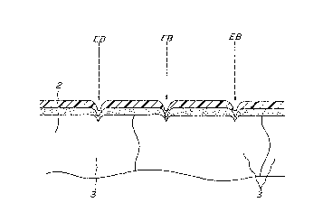
Flg. 2 ls a dlagrammatlcal vlew showlng permeatlon
force ln depthwlse dlrectlon and magnltude thereof ln
wldthwlse dlrectlon by varlous methods to the slllcon steel
sheet;
Flgs. 3a, 4a and 5a are schematlc vlews showlng
electron beam ~EB) lrradlated tracks, respectlvely;
Flgs. 3b, 4b and 5b are vlews showlng an lntenslty
of EB, respectlvely;
Flg. 6 ls a dlagrammatlcal vlew of EB
7b
,~ ,
~ ~ 64881-343
2~ ~ ~2~ 3
irradiation apparatus usable for carrying out the
invention;
Fig. 7a is a schematic view showing EB
irradiated tracks on the sheet surface: and
05 Figs. 7b and 7c are views showing intensity of
EB in the widthwise direction of the sheet during the
scanning of EB by various methods, respectively.
The invention will be described with respect to
experimental details resulting in the success of the
invention.
A slab of silicon steel containing C: 0.043% by
weight (hereinafter referred to as % simply), Si: 3.45%,
Mn: 0.068%, Se: 0.022%, Sb: 0.025% and Mo: 0.013% was
heated at 1380~C for 4 hours and hot rolled to form a
hot rolled sheet of 2.2 mm in thickness, which was then
cold rolled two times through an intermediate annealing
at 980~C for 120 minutes to obtain a final cold rolled
sheet of 0.20 mm in thickness. Next, the cold rolled
sheet was subjected to decarburization and primary
recrystallization annealing in a wet hydrogen atmosphere
at 820~C, coated with a slurry of an annealing separator
consisting mainly of MgO, subjected to secondary
recrystallization annealing at 850~C for 50 hours to
preferentially grow the secondary recrystallized grains
in Goss orientation and then subjected to purification
annealing at 1200~C in a dry hydrogen atmosphere for
Z()~ 3
5 hours to obtain a sample sheet (A). Furthermore, an
insulative layer consisting mainly of phosphate and
colloidal silica was formed on a part of the sample
sheet (A) to obtain a sample sheet (B). Thereafter, the
05 following treatments (1)-(4) were applied to each of the
sample sheets (A) and (B), whereby microstrains or
microareas were locally produced in a direction
perpendicular to the rolling direction of the sheet at
an interval of 8 mm.
(1) cutting with a knife;
(2) YAG laser irradiation (energy per spot: 4x10⁻³J,
spot diameter: 0.15 mm, distance between spot centers:
0.3 mm, scanning interval: 8 mm);
(3) EB irradiation (acceleration voltage: 100 kV,
current: 0.7 mA, spot diameter: 1.0 mm, distance between
spot centers: 0.3 mm, scanning interval: 8 mm);
(4) EB irradiation (acceleration voltage: 100 kV,
current: 3.0 mA, spot diameter: 0.15 mm, distance
between spot centers: 0.3 mm, scanning interval: 8 mm).
Each of the above treated samples was subjected
to strain relief annealing at 800~C for 2 hours.
The magnetic properties measured after the strain relief
annealing are shown in the following Table 1.
For the comparison, the magnetic properties of
non-treated sheet (no introduction of microarea, strain
relief annealing) are also shown in Table 1.
Z()~Z~3
Table 1
\ FAinish Formation of Magnetic
Treatme ~ ansnheeaelted laYer on finish B (T) W (W/k )
O - 1.92 0.87
(1)
- O 1.91 0.86
O - 1.92 0.85
(2)
- O 1.91 0.84
O - 1.92 0.80
(3)
- O 1.92 0.79
O - 1.92 0.79
(4)
- O 1.91 0.78
, O - 1.92 0.85
Comparatlve
sheet _ O 1.91 0.86
As seen from Table 1, when each of the sample
sheets (A) and (B) is subjected to each of the treat-
ments (3) and (4), the iron loss value is improved by
0.05-0.08 W/kg as compared with those of the other
cases.
In the sample sheets treated by the treatment
(4), micro-convex areas were observed at the rear
surface of the sheet, from which it is understood that
the pushed microareas are introduced up to the rear
surface of the sheet.
The reason why the iron loss value of the sample
- 10 -
~n~ 3
treated by the treatment (3) is improved as compared
with those treated by the treatments (l) and (2) is due
to the fact that as shown in Fig. la, microareas of
forsterite layer 1 and insulative layer 2 pushed into
05 base metal 3 (secondary recrystallized grains having a
Goss orientation) in depthwise direction thereof act as
a nucleus for effective refinement of magnetic domains
even when being subjected to strain relief annealing,
whereby the magnetic domain refinement is made possible.
Further, the reason why the iron loss value of
the sample treated by the treatment (4) is considerably
improved as compared with those of the other samples is
due to the fact that as shown in Fig. lb, the pushed
microareas are further penetrated in the base metal 3 to
extend up to the rear surface of the sheet, which act as
a strong nucleus for the magnetic domain refinement.
Moreover, the deep penetration of the microareas
of the forsterite layer and insulative layer into the
inside of the base metal in the widthwise direction of
the sheet can be first achieved by using EB having a
high voltage of 65-500 kV and a low current of
0.001-5 mA. As shown in Fig. 2, the use of high voltage
and low current EB is strong in the permeation force in
depthwise direction and narrow in the permeation width
as compared with the other means (laser, plasma,
mechanical means and the like), so that the forsterite
- 11 -
2()~
layer and insulative layer can be pushed into the base
metal without disappearance.
Then, EB irradiating conditions will be
described with respect to the following experiment.
05 A slab of silicon steel containing C: 0.042%,
Si: 3.42%, Mn: 0.072%, Se: 0.021%, Sb: 0.023% and
Mo: 0.013% was heated at 1370~C for 4 hours and hot
rolled to form a hot rolled sheet of 2.2 mm in
thickness, which was then cold rolled two times through
an intermediate annealing at 980~C for 120 minutes to
obtain a final cold rolled sheet of 0.20 mm in
thickness. After the cold rolled sheet was subjected to
decarburization and primary recrystallization annealing
at 820~C in a wet hydrogen atmosphere, a slurry of an
annealing separator consisting mainly of MgO was applied
to the sheet surface and then the sheet was subjected to
secondary recrystallization annealing at 850~C for
50 hours to preferentially grow the secondary
recrystallized grain in Goss orientation and then
subjected to purification annealing at 1200~C in a dry
hydrogen atmosphere for 5 hours to obtain a sample sheet
(C). Furthermore, an insulative layer consisting mainly
of phosphate and colloidal silica was formed on a part
of the sample sheet (C) to obtain a sample sheet (D).
Thereafter, the following EB irradiation treatments
(1)-(3) were applied to each of the sample sheets (C)
-12-
znnl~3
and (D), whereby microareas were locally produced in a
direction perpendicular to the rolling direction of the
sheet at an interval of 8 mm.
(1) EB irradiation (acceleration voltage: 150 kV,
05 current: 1.5 mA, spot diameter: 0.12 mm, distance
between spot centers: 0.3 mm, scanning interval: 8 mm)
As the EB irradiation to the steel sheet
surface, the irradiated diameter of each spot and the
irradiated distance between spots were made uniform as
shown in Fig. 3a. Moreover, Fig. 3b shows an intensity
of EB at each spot as a height of triangle.
(2) EB irradiation (acceleration voltage: 150 kV,
current: 1.5 mA or 0.75 mA, spot diameter: 0.12 mm or
0.80 mm, distance between spot centers: 0.3 mm, scanning
interval: 8 mm)
As the EB irradiation to the steel sheet
surface, the irradiated tracks as shown in Fig. 4a were
formed by alternately changing the current to 1.5 mA and
0.75 mA to change the irradiated diameter and the
irradiated distance. Moreover, Fig. 4b shows an
intensity of EB likewise Fig. 3b.
(3) EB irradiation (acceleration voltage: 150 kV,
current: 1.5 mA or 0.75 mA, spot diameter: 0.12 mm or
0.80 mm, distance between spot centers: 0.3 mm, scanning
interval: 8 mm)
As the EB irradiation to the steel sheet
20~ 3
surface, the irradiated tracks as shown in Fig. 5a were
formed by changing the irradiated diameter and the
irradiated distance with currents of 1.5 mA and 0.75 mA.
Moreover, Fig. 5b shows an intensity of EB likewise
Fig. 3b.
Each of the above treated samples was subjected
to strain relief annealing at 800~C for 2 hours.
The magnetic properties measured after the strain relief
annealing are shown in the following Table 2.
For the comparison, the magnetic properties of
non-treated sheet (no introduction of microarea, strain
relief annealing) are also shown in Table 2.
Table 2
\ (C) Formation of MagnetiC properties L
Finish
\ 1 d insulative factor
Treatm ~ annealed sheet 10 17/50 g
O - 1.92 O.ô2 96.6
(1)
- O 1.91 0.83 96.7
O - 1.92 0.78 96.7
(2)
- O 1.91 0.79 96.8
O - 1.92 0.77 96.7
(3)
- O 1.91 0.78 96.ô
. O - 1.92 0.88 96.7
Comparatlve
sheet O 1.91 O.ô9 96.8
- 14 -
zns)~
As seen from Table 2, in the sample sheets (C)
and (D) treated through EB, the iron loss value is
improved by 0.05-0.11 W/kg as compared with those of the
comparative sheet. Particularly, the iron loss value in
05 case of the EB irradiation treatments (2) and (3) is
largely improved by 0.10-0.11 W/kg. Furthermore, the
products have a good lamination factor of 96.6-96.8~.
Further, it has been found that the permeation
force of EB in the thickness direction (depthwise
direction) of the silicon steel sheet increases at an
acceleration voltage of not less than 65 kV usually
generating a great amount of X-ray. In general, the
acceleration voltage usually used for welding is not
more than 60 kV, so that the permeation force is very
small. That is, the above effect found out in the
invention can not be found and utilized at such a
conventional acceleration voltage. In order to utilize
the effect of the invention at maximum, therefore, it is
important to set the acceleration voltage to a high
value (65-500 kV) and the acceleration current to a
small value (0.001-5 mA), whereby the permeation force
in the thickness direction of the silicon steel sheet
can be increased without causing the breakage of the
forsterite layer and insulative layer. Further, in
order to efficiently conduct the magnetic domain
refinement, it is favorable that the diameter of the
- 16-
zn~ 3
irradiated area is rendered into 0.005-0.3 mm by using a
fine EB. And also, it is preferable that the direction
of scanning EB is substantially perpendicular to the
rolling direction of the sheet, preferably an angle of
05 60-90~ with respect to the rolling direction, and the
distance between spot centers is 0.005-0.5 mm, and the
scanning interval is 2-20 mm, and the irradiation time
per spot is 5-500 ~sec. Moreover, the insulating
property on the EB irradiated tracks may be enhanced by
forming the insulative layer after the EB irradiation,
but in this case the cost is increased. In general, the
satisfactory insulating effect can be developed without
the formation of insulative layer after EB irradiation.
The silicon steel sheets according to the inven-
tion may be used as a material for stacked lamination-
core type transformers and wound-core type transformers
as previously mentioned. In case of the stacked
lamination-core type transformer, the introduction of
microarea having a smaller spot diameter is required as
compared with the wound-core type transformer. For this
purpose, it is favorable that the current is small and
the scanning interval is wide as EB irradiating
conditions. In case of the wound-core type transformer,
it is favorable that the current is somewhat large and
the scanning interval is narrow as the EB irradiating
conditions for promoting the introduction of microarea.
-16-
Z(l ~ 3
Moreover, EB may be irradiated to one-side surface or
both-side surfaces of the silicon steel sheet.
In Fig. 6 is schematically shown a preferable
embodiment of the EB irradiation apparatus suitable for
05 practicing the invention, wherein 11 is a high voltage
insulator, 12 an EB gun, 13 an anode, 14 a column valve,
15 an electromagnetic lens, 16 a deflecting coil, 17 an
EB, 18 a grain oriented silicon steel sheet and 19 and
20 discharge ports, respectively.
In general, the EB irradiation to the steel
sheet surface is carried out in a direction substan-
tially perpendicular to the rolling direction of the
sheet as shown in Fig. 7a. In this case, since the
current of the electromagnetic lens (focusing current)
is constant, when the focus of the electromagnetic lens
is met with the center of the sheet in the widthwise
direction, the EB intensity is strongest at the central
portion (17-2') of the sheet in the widthwise direction
thereof and becomes weak at both end portions (17-1',
17-3') of the sheet as shown in Fig. 7b because when the
focusing position of EB locates on the steel sheet
surface, the pushing into the sheet is carried out most
effectively.
In the preferred embodiment of EB irradiation
according to the invention, the focusing distance of EB
is corrected in accordance with the change of the
zn~ .3
distance between electromagnetic lens and the sheet
during the EB scanning so as to always meet the focusing
position with the sheet surface over the widthwise
direction thereof. Such a correction of the focusing
05 distance can be accurately carried out by dynamically
controlling the currents of the electromagnetic lens 15
and the deflecting coil 16 shown in Fig. 6, whereby the
EB scanning can be conducted at the same EB intensity
over the full width of the sheet as shown in Fig. 7c.
Such a treatment is called as a dynamic focusing
hereinafter.
In this connection, the invention will be
described with respect to the following experiment.
A slab of silicon steel containing C: 0.043%,
Si: 3.39%, Mn: 0.066%, Se: 0.020%, Sb: 0.023% and Mo:
0.015% was heated at 1360~C for 4 hours and hot rolled
to form a hot rolled sheet of 2.0 mm in thickness, which
was then subjected to a normalized annealing at 950~C
for 3 minutes and further cold rolled two times through
an intermediate annealing at 950~C for 3 minutes to
obtain a final cold rolled sheet of 0.20 mm in thickness.
After the cold rolled sheet was subjected to
decarburization and primary recrystallization annealing
at 820~C in a wet hydrogen atmosphere, a slurry of an
annealing separator consisting mainly of MgO was applied
to the sheet surface, and then the sheet was subjected
-18-
zn~2~.3
to finish annealing.
After an insulative layer consisting mainly of
phosphate and colloidal silica was formed on the sheet
surface, the sheet was subjected to usual EB irradiation
05 (a-l) or EB irradiation through dynamic focusing (a-2).
For the comparison, there was provided the sheet not
subjected to EB irradiation (a-3).
On the other hand, a slurry of an annealing
separator consisting mainly of Al2O3 was applied to the
sheet surface after the above primary recrystallization
annealing, which was subjected to finish annealing under
the same conditions as mentioned above. Thereafter, the
finish annealed sheet was lightly pickled and subjected
to an electrolytic polishing into a mirror surface
having a center-line average roughness of Ra = 0.l ~m,
on which a thin layer of TiN having a thickness of
l.0 ~m was formed by an ion plating apparatus through
HCD method (acceleration voltage: 70 V, acceleration
current: l000 A, vacuum degree: 7x10⁻⁴ Torr). Then, the
sheet was subjected to usual EB irradiation (b-l) or EB
irradiation through dynamic focusing (b-2) and an
insulative layer consisting mainly of phosphate and
colloidal silica was formed thereon.
Moreover, an insulative layer consisting mainly
Of phosphate and colloidal silica was formed on a part
of the sheet provided with the TiN thin layer, which was
- 19 -
zn~ t.~
subjected to usual EB irradiation (b-3) or EB irradia-
tion through dynamic focusing (b-4).
For the comparison, there was provided the sheet
provided with the insulative layer but not subjected to
05 EB irradiation treatment (b-5).
The magnetic properties of each of the thus
obtained products are shown in the following Table 3.
-20-
?Jt .
Table 3
Treatment Sample EB irradiation Magnetic properties
method Blo(T) W17/50(W/kg)
a-l (9 usual EB 1. 90 O . 82
irradiation *
Finish annealed ~ EB irradiation
a-2 sheet through dynamic 1.91 0.78
focusing **
a-3 ~3 1.90 0.85
b-l (9 usual EB 1 .92 0.66
irradiation *
~ EB irradiation
b-2 Sheet provided at through dynamic 1.93 0.63
its surface with focusing **
b-3 TiN layer aft;r (9 usual EB 1. 92 0.67
of finish
annealed sheet ~ EB irradiation
b-4 through dynamic 1.93 0.64
focusing **
b-5 ~3 1.92 0.70
* ~9 usual EB irradiation : acceleration voltage: 70 kV,
acceleration current: 7 mA,
scanning interval in a direction
perpendicular to rolling direction:
300 ~m, scanning width: 10 mm.
** ~3 EB irradiation through
dynamic focusing: acceleration voltage: 70 kV,
acceleration current: 7 mA,
scanning interval in a direction
perpendicular to rolling direction:
300 ~m, scanning width: 10 mm,
dynamic focusing of electromagnetic
lens and deflecting coil.
As seen from Table 3, when the sheet is
subjected to EB irradiation through dynamic focusing,
-21-
;Z(~S~
the iron loss property is further improved as compared
with the case of conducting the usual EB irradiation.
Thus, the further reduction of iron loss can be
attained by adopting the dynamic focusing in the
05 widthwise direction of the sheet when the sheet provided
with the insulative layer after the finish annealing of
the grain oriented silicon steel sheet is subjected to
EB irradiation or the sheet provided with TiN layer
after the mirror polishing of the finish annealed sheet
is subjected to EB irradiation before or after the
formation of the insulative layer. That is, in case of
the dynamic focusing, the focusing distance of the
electron beam is corrected so as to always locate at the
sheet surface in accordance with the change of the
focusing position during the EB scanning as shown in
Fig. 7c, whereby constant irradiated tracks are formed
over the widthwise direction of the sheet to effectively
conduct the refinement of magnetic domains over the
whole area of the sheet, and consequently low iron loss
silicon steel sheets can be obtained.
The following examples are given in illustration
of the invention and are not intended as limitations
thereof.
Example l
z5 A slab of each of (A) silicon steel containing
C: 0.043~, Si: 3.36%, Se: 0.02~, Sb: 0.025% and
zn~
Mo: 0.013~ and (B) silicon steel containing C: 0.063~,
Si: 3.42%, Al: 0.025%, S: 0.023~, Cu: 0.05~ and Sn: 0.1%
was heated at 1380~C for 4 hours and hot rolled to
obtain a hot rolled sheet of 2.2 mm in thickness, which
05 was then cold rolled two times through an intermediate
annealing at 980~C for 120 minutes to obtain a final
cold rolled sheet of 0.20 mm in thickness. After the
cold rolled sheet was subjected to decarburization and
primary recrystallization annealing at 820~C in a wet
hydrogen atmosphere, a slurry of an annealing separator
consisting mainly of MgO was applied to the surface of
the sheet, which was then subjected to a finish
annealing, wherein secondary recrystallization annealing
was carried out at 850~C for 50 hours to preferentially
grow secondary recrystallized grains in Goss orientation
and purification annealing was carried out at 1200~C in
a dry hydrogen atmosphere for 5 hours, whereby a finish
annealed sheet (thickness: 0.20 mm) provided with a
forsterite layer was obtained. Further, a part of the
sheet was provided at its surface with an insulative
layer.
These sheets were subjected to EB irradiation in
a direction perpendicular to the rolling direction of
the sheet by means of EB irradiation apparatus under
conditions that acceleration voltage was 100 kV,
acceleration current was 0.5 mA, spot diameter was
-23-
2(1~P~Z,11 3
0.1 mm, distance between spot centers was 0.3 mm and
scanning interval was 8 mm, provided that the microareas
pushed did not reach to the layers at the rear surface
of the sheet.
After the sheet was subjected to strain relief
annealing at 800~C for 2 hours, the magnetic properties
were measured to obtain results as shown in the follow-
ing Table 4 together with those of the comparative sheet
~no introduction of microarea, strain relief annealing).
As seen from Table 4, the iron loss Wl7/50 is reduced by
0.08-0.1 W/kg as compared with that of the comparative
sheet.
Table 4
\ Insulative Magnetic properties
\ Finish layer formed EB
\ annealed on finish irradiation
Sample\ annealed sheet BlO(T) W17/50 ~W/kg)
O - 1.92 0.79
(A)
- O 1.91 0.77
irradiated
O - 1.94 0.78
(B)
- O 1.93 0.76
Compar- O _ 1.92 0.86 not
ative irradiated
sheet - O 1.91 0.87
Example 2
A slab of each of (A) silicon steel containing
C: 0.042%, Si: 3.38%, Se: 0.023%, Sb: 0.026% and
-24-
~n~?~Z1.3
Mo: 0.012% and (B) silicon steel containing C: 0.061%,
Si: 3.44%, Al: 0.026~, S: 0.028%, Cu: 0.08% and
Sn: 0.15% was treated by the same manner as in Example 1
to obtain a finish annealed sheet (thickness: 0.20 mm)
05 provided with a forsterite layer. Further, a part of
the sheet was provided at its surface with an insulative
layer.
These sheets were subjected to EB irradiation
according to the scanning shown in Fig. 5 in a direction
perpendicular to the rolling direction of the sheet by
means of EB irradiation apparatus under conditions that
acceleration voltage was 150 kV, acceleration current
was 1.5 mA, spot diameter was 0.1 mm or 0.7 mm, distance
between spot centers was 0.3 mm and scanning interval
was 8 mm, provided that the microareas pushed reached to
the layers at the rear surface of the sheet.
After the sheet was subjected to strain relief
annealing at 800~C for 2 hours, the magnetic properties
were measured to obtain results as shown in the
following Table 5 together with those of the comparative
sheet (no introduction of microarea, strain relief
annealing). As seen from Table 5, the iron loss W17/50
is reduced by 0.10-0.14 W/kg as compared with that of
the comparative sheet.
- 25-
~nn~,?~
Table 5
\ Insulative Magnetic properties
\ Finish layer formed EB
\ annealed on finish irradiation
Sample \ annealed sheet BlO(T) W17/50 (W/kg)
O - 1.92 0.78
(A)
- O 1.91 0.76
irradiated
O - 1.94 0.77
(B)
- O 1.93 0.75
Compar- O _ 1.92 0.88 not
ative irradiated
sheet - O 1.91 0.89
Example 3
A slab of each of (A) silicon steel containing
C: 0.040%, Si: 3.45%, Se: 0.025%, Sb: 0.030% and
Mo: 0.015% and (B) silicon steel containing C: 0.057%,
Si: 3.42%, sol Al: 0.026%, S: 0.029%, Cu: 0.1% and
Sn: 0.050% was heated at 1380~C for 4 hours and hot
rolled to obtain a hot rolled sheet of 2.2 mm in
thickness, which was then cold rolled two times through
an intermediate annealing at 1050~C for 2 minutes to
obtain a final cold rolled sheet of 0.20 mm in
thickness. After the cold rolled sheet was subjected to
decarburization and primary recrystallization annealing
at 840~C in a wet hydrogen atmosphere, a slurry of (a)
an annealing separator consisting mainly of MgO or (b)
an annealing separator consisting of A1203: 6096,
- 26-
;2n~ J1.3
MgO: 35%, ZrO2: 3~ and TiO2: 2% was applied to the
surface of the sheet.
After the application of the annealing separator
(a), the sheet (A) was subjected to secondary
05 recrystallization annealing at 850~C for 50 hours and
further to purification annealing at 1200~C in a dry
hydrogen atmosphere for 5 hours, while the sheet (B) was
subjected to secondary recrystallization annealing by
heating from 850~C to 1050~C at a rate of 10~C/hr and
further to purification annealing at 1220~C in a dry
hydrogen atmosphere for 8 hours.
Then, an insulative layer consisting mainly of
phosphate and colloidal silica was formed on the surface
of each of these sheets.
On the other hand, each of the sheets after the
application of the annealing separator (b) was pickled
to remove oxides from the surface and subjected to
electrolytic polishing into a mirror state, on which was
formed a TiN tension layer of 1.0 ~m in thickness by
means of an ion plating apparatus and further the same
insulative layer as mentioned above was formed thereon.
Thereafter, each of these sheets was subjected
to EB irradiation through dynamic focusing by means of
the apparatus shown in Fig. 6 at an interval of 8 mm in
a direction perpendicular to the rolling direction of
the sheet under conditions that acceleration voltage was
~nn~.3
70 kV, current was 10 mA and scanning interval was
200 ~m. Then, the magnetic properties were measured to
obtain results (average values in the widthwise
direction of the sheet) as shown in the following
Table 6.
Table 6
Magnetic
Kind Annealing Surface layerproperties
Of separator
steel Blo(T)Wl7/so(W/kg)
a only insulative layer 1.91 0.78
A
b TiN+insulative layer 1.93 0.63
a only insulative layer 1.93 0.79
B
b TiN+insulative layer 1.94 0.64
As mentioned above, the invention provides grain
oriented silicon steel sheets not degrading iron loss
property even through strain relief annealing and a
method of stably producing the same.
- 28-