Note: Descriptions are shown in the official language in which they were submitted.
2001~58
TITLE OF THE INVENTION
Device for calibrating and testina rina-shaped current
clamps
BACKGROUND OF THE INVENTION
Field of the Invention
The invention relates to a device for calibrating and
testing ring-shaped current clamps, comprising a calibra-
tion housing with an outer conductor enclosing the
current clamp and an inner conductor passing through the
current clamp.
Discussion of Backaround
Current clamps can be divided into measuring clamps and
current in~ection clamps. ~easuring clamps act as
current transformers and current in~ection clamps as
transformer with a secondary winding. They are mainly
used in the fields of EMC, EMP, lightning testing, ESD
and EMI control.
Current clamps are very sensitive to overloading. The
inbuilt terminating resistors can be easily destroyed or,
worse, damaged if the currents are too high. Damaged
resistars cannot be easily detected and may falsify the
measurements unnoticed.
From the point of view of quality control, it is there-
fore important to be able to measure the freauency
response of such current clamps. For these purposes, the
firm EATON CORPORATION, 5340 Alla Road, Los Angeles
. - : -
: . . -.: . . - .
. -. . , I
. : . : . - - - . ; . - ; .
:- : .. ....... .
2001258
- 2 -
CA 90066, for example, offers a so-called calibration
jig. This device essentially consists of an open hou~ing
and an inner conductor which is enclosed by the current
clamp during testing. However, measurements have shown
that this test device is unusable ~or higher frequencies
from several hundred MHz to 1 GHz.
SU~MARY OF THE INVENTION
Accordingly, one ob~ect of this invention is to provide
a novel device for calibrating and testing ring-shaped
current clamps, comprising a calibration housing with an
outer conductor enclosing the current clamp and an inner
conductor passing through the current clæmp, by means of
which the frequency response can be precisely measured in
the RF range. -
According to the invention, the solution consists in
that, in a device of the type lnitially mentioned, the
outer conductor encloses the current clamp on all sides
and is adapted to the shape of the current clamp and that
the calibration housing with the current clamp accom-
modated therein exhibits an impedance which is predeter-
mined by a measuring system.
The core of the invention lies in the fact that the
current clamp to be tested is completely closed off from
the outside world. The calibration housing with the
current clamp accommodated therein has an impedance which
matches the surrounding measuring device at any point.
As a result, a measuring signal only senses the distur-
bance created by the current clamp. It is thus only due
to the invention that it has become possible to mea~ure
the frequency response accurately up to 1 GHz. This
~ results in advantages
i
for quality assurance,
2. for error correction in high-precision measurements,
,. ..
~,
.. ,:: . .
.- . . , ~ -............ - , ~
~001258
- 3 -
3. for optimum utilization of the current clamps (that
i8 to say up to the maximum individual loading
limit) and
4. for the detection of damage.
Advantageous embodiments of the invention are found in
the dependent patent claims.
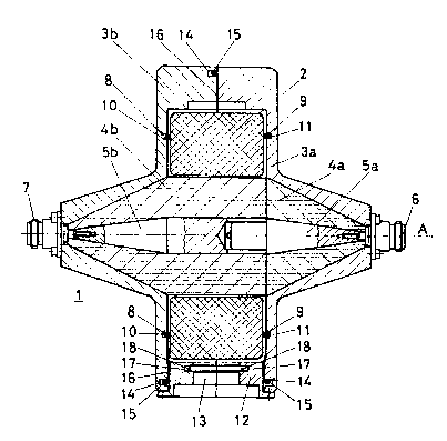
BRIEF DESCRIPTION OF THE DRAWINGS
A more complete appreciation of the invention and many of
the attendant advantages thereof will be readily obtained
as the same becomes better understood by referenGe to the
following datailed description when considered in connec-
tion with the accompanying drawing, wherein the sole
figure shows a longitudinal section of a calibration
housing according to the invention with a current clamp
accommodated therein.
DESCRIPTION OF THE PREFERRED ENBODIMENTS
Referring now to the drawing, the sole figure shows a
longitudinal section through a calibration housing 1.
According to a preferred embodiment, this consists of two
halves which can be ~oined together in the axial
direction. Correspondingly, certain electrical elements
of the calibration housing 1 are assembled from two
parts. In the figure, the parts belonging together in
each case are designated by a and ~ piaced behind the
reference number.
The calibration housing 1 is mechanically adapted to the
constructional shape of a type of current clamp 2 to be
tested.
The current clamp is not part of the inven$ion but, for
example, a commercially available measuring clamp for
, 1 :, . . . : , ,
- : : .
. ~ , .. . : , : . . , . . , ,
.. , ~ ; . , ., ,,, ~ - ~ : . ...
, :. , . . ~ . ,- . . ,
X0012S8
-- 4 --
radio frequency applications. It i8 ring-shaped and has,
for example, a hinge and a clo8ing mechanism so that it
can be placed around an electric conductor in the form of
a clamp. On the outside a connection is mounted, for
S example a ~tandard socket.
The calibration housing 1 comprises an outer conductor
3a, 3b, an insulator 4a, 4b and an inner conductor Sa,
5b. It is approximately rotationally symmetrical with
respect to an axis A. On this axis A, two connections 6
and 7 are provided in each case at opposite ends of the
calibration housing 1.
The outer conductor 3a, 3b completely encloses the
current clamp 2. It is also adapted to the external
shape of the latter. The inner conductor 5a, 5b is
passed through the current clamp 2. The insulator 4b is
arranged between inner conductor 5b and current clamp 2.
Inner conductor 5b and insulator 4~ are cylindrical
inside the current clamp 2. The in~ulator 4b has an
outqide diameter D which precisely corresponds to the
inside diameter of the current clamp, an inside diameter
d which precisely corresponds to the diameter of the
inner conductor 5b, and a dielectric constant e,. These
three variables satisfy the foll~wing relation:
D
ZL = --- ln - (I)
16, d
ZL is an impedance which is predet~rmined by a measuring
system (for example zl = 50 ohms).
The insulator 4a, 4b centers the inner conductor Sa, 5b
with respect to the ring-shaped current clamp 2. It
should consist of a material which is sufficiently solid.
So that the inside diameter d and, in consequence, the
inner conductor 5a, 5b is as small as possible, the
dielectric con~tant ~, is preferably selected to be of the
order of magnitude of one. ~eflon is advantageous in
'"~: ' `~ '.; ' '
- . .
:~
. . . .
` Z001258
-- 5 --
this respect, as are ~foam-like" materials, that i8 to
say materials containing a large volume of air, such as
expanded polystyrene.
The two axially arranged connections 6 and 7 are, for
S example, standard connectors for coaxial cables. In
general, the inside diameter of the current clamp 2 and
the diameter of the inner conductor Sa, 5b are therefore
greater than the corresponding dimensions of the standard
connector. According to the invention, a transition is
provided for each connection 6, 7 in this case. In this
transition, inner and outer conductors are in each case
conically tapered from the axial area of the current
clamp 2 towards the connections 6, 7 along a length L.
The important factor in this is that the relation (I) is
maintained at every point of the transition. (The
maximum outside diameter D is then replaced by a local
outside diameter in the formula (I). Thi~ correspond-
ingly applies to the inside diameter d.)
The smaller the angle of inclination, that is to say the
ratio batween outside diameter D and length L, the better
the transition and the lower the effect of mechanical
inaccuracies of the components. On the other hand, it is
desirable for economic reasons to keep the calibration
housing as small as possible. It has been found that it
is advantageous to select the length L to be of approxi-
mately the same size as th~ outside diameter D. ~he
length L is preferably at least as large as the maximum
outside diameter D.
The current clamp 2 must be electrically insulated from
the outer conductor 3a, 3b. At the same time, it should
be mechanically well fixed in place. According to a
preferred embodiment of the invention, this is achieved
in such a manner that each half of the outer conductor 3a
and 3b, respectively, exhibits an annular slot 8 and 9,
respectively, into which an elastic O ring 10 and 11,
respectively, is inserted. The outer conductor 3a, 3b
-. - . : - . ; . . . . ~ - : ., .
2001258
-- 6 --
comes into eontact with the current clamp 2 at exactly
one place, namely at its conneetion 13. The electrical
contact i8 secured by a slot 17 and an elastic band 18
around which wire is wound and which is inserted therein.
For the connection 13 of the current clamp 2 mentioned at
the beginning, a mounting plate 12 i9 inserted at the
outer eonduetor 3a, 3b.
The two halves of the ealibration housing must be ~oined
to one another in sueh a manner that proper eleetrie
contact is ensured. In the ease of the inner conduetor
5a, 5b, this is aehieved most simply by means of a plug-
in contact. In the ease of the outer eonductor 3a, 3b,
one of the halves is preferably provided at one eontact
face 16 with.a eontinuous slot 14 into whieh an elastie
band 15, around whieh wire i8 wound (for example a rubber
ring around whieh a wire mesh is wound, ealle~ a gasket)
is inserted.
If the ealibration housing is fabrieated of aluminum
aecording to an advantageous embodiment, the eontaet faee
20 iS al80 eovered with a layer of good eonduetivity (for
example of silver).
Naturally, the ealibration housing aeeording to the
invention has dimensions whieh are different depending on
the eonstruetional shape of the eurrent elamp to be
tested. In the ease of small eurrent elamps, the eonieal
transition may be omitted, depending on eireumstanees.
It is not so important that the ealibration housing
eonsists of two halves whieh ean be ~oined togethe~
axially. In praetiee, attentien must simply be paid to
the faet that the measures whieh allow the housing to be
taken apart do not induce any disturbanees in the imped-
anee and no inadmissible wave modes are propagated in the
test deviee.
20012S8
It can finally be said that the invention creates a
mechanically simple device by means of which current
clamps can also be electrically qualified in the RF
range.
Obviously, numerous modifications and variatlons of the
present invention are po~sible in light of the above
teachings. It is therefore to be understood that, within
the scope of the appended claims, the invention may be
practiced otherwise than as specifically described
herein.
. ,, .,, , . , , . ,.,, .. ; , : : . , ~ . . .
,.~ ,, ; .~ ...... ....~,. . -- .: ' ' . :
: ~ . : .. ~ . . , . : . . .
. . .. . . .