Note: Descriptions are shown in the official language in which they were submitted.
392
METHOD AND APPARATUS FOR PREVENTING PARASITIC
ELECTRICAL DISCHARGES IN MAGNETIC DISK DRIVES
Field of the Invention
This invention relates generally to electrical
protection circuitry for magnetic disk drives and more
particularly to such circuitry which is operable to prevent
the unwanted parasitic electrical discharge between a
5 read/write head and a magnetic disk to which it is coupled.
Back~round Art
In conventional sensing and electronic drive circuitry
for connection to and operation with the read/write heads of
magnetic disk drives, the magnetic core of the head is
10 magnetically coupled to and insulated from a winding which in
turn is connected to an amplifier. The amplifier is adapted
; to either amplify read signals taken from a magnetic disk or
to amplify write signals applied to the read/write head of the
disk drive. The winding is typically insulated from the other
f 15 elements of the read/write head by a polymer, such as a
photoresist, which will have a resistance typically on the
order of 1000 Megohms. As is well known, the read/write head
is positioned closely adjacent to the surface of the magnetic
disk sur~ace, and these closely spaced devices form two plates
20 of a parasitic capacitance. This parasitic capacitance may
thus be charged with a current drawn through the resistance of
the above insulating material located between the winding and
the other elements of the read/write head.
The problem caused by the above parasitic RC circuit
25 is that the charged parasitic capacitance will frequently
discharge during a read operation o~ the disX drive and
thereby produce an error in the read data. This discharge
takes place in either one of two modes. In one mode, the
discharge kakes place randomly over the surface of the disk,
30 in which case it has been re~erred to as an "electrical
storm". In the other mode, the discharge will take place
Case 139031
:
;,: .
.
.. . .
Z ~ 3~
repeatedly at a surface irregularity on the disk every time
the irregularity passes underneath the read/write head. The
latter mode has been referred to as the "~ilton effect".
Prior efforts have been made to solve this problem and
they involve reducing the DC bias applied to the above
described amplifier in order to reduce the DC voltage across
the head-to-disk surface parasitic capacitance. However, this
approach has not proven satisfactory because of the DC biasing
levels required for normal and acceptable amplifier operation
with magnetic disk drives whPre only positive voltage supplies
are available.
Disclosure of Invention
It is an object of the present invention to eliminate
the above problem of electrical discharge between the
read/write head and the magnetic disk surface of a magnetic
disk drive. This object is achieved by biasing the magnetic
disk surface to the same or approximately the same DC voltage
level as is applied to the winding of the read/write head.
Thus, in this manner both "plates" of the above parasitic
capacitance between the magnetic disk surface and the
read/write core are at the same DC voltage level, and no
charging of this parasitic capacitance is now possible.
Therefore, the claims according to the present
invention for preventing the above described undesirable
electrical discharge between the read/write head and its
associated magnetic disk involve a means and method for
applying a DC voltage to the disk surface which is
approximately equal to the DC voltage applied to the windings
of the read/write head, and this action in turn prevents the
above parasitic capacitance from ever charging.
The invention described herein has a wide application
and utility in many different types of disk drives, and has
been found to be particularly useful on the Hewlett Packard
760 megabyte -5 1/4 inch fixed disk drive known as the model
no. HP9754X disk drive.
Case 189031
::: : ,. . : .
... ., .. .. . : ~ ..... . . ..
,.. : :. : , .: :
. . .- ~ . . . . .
. ' `
:,
. . :
:~
~o~9~
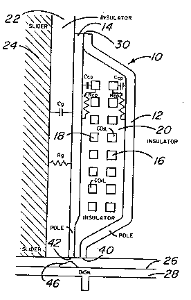
Brief Descri~ion of the Drawinq
~ig. 1 is a cross-section view of a magnetic core
read/write head assembly shown adjacent to a magnetic disk
surface to which it is magnetically coupledO
5Fig. 2 is an electrical equivalent circuit for ths
magnetic head assembly of Fig. 1.
Detailed Dascription
Referring now to Fig. 1, the magnetic head is
designated generally as lO and includes typically a pair of
outer magnetic pole pieces 1~ and 14 connected in the
configuration shown to surround two layers of coils 16 and 18.
These two layers o~ coils 16 and 18 are insulated from each
other and from the outer core mPmbers 12 and 14 by an
insulaking material 20 which will typically be a polymer
material such as photoresist. The head memher 10 also
includes an insulating layer 22 which supports the pole piece
14 and which in turn is disposed on a slider 24 used for
moving the head 10 from location to location across the
surface 26 of a magnetic layer 28. The two pole pieces 12 and
14 are bonded together at the interface region 30.
Within the insulating material 20 of the magnetic
read/write head 10 there is a parasitic coil-to-pole
capacitance, designated Ccp, and a parasitic resistance, Rcp~
as indicated in Fig. 1. The insulating layer 22 will also
possess a parasitic capacitance, Cgr and a parasitic
resistance, R~, as indicated in Fig. 1, and these parasitic
values of resistance and capacitance are shown in equivalent
circuit form in Fig. 2 together with Rcp and C~p. The
read/write head 10 in Fig. 1 as well as a magnetic disk to
which it is coupled may be fabricated using processes known to
those skilled in the art. Such processes are disclosed, ~or
example, in the Hewlett-Packard Journal, Vol. 36, No. 11,
November 1985, incorporated fully herein by reference.
Referring now to Fig. 2, the two parameters Rc indicate
the resistance of the two layers 16 and 18 of coil in the head
Case 189031
` ::
~: :: ' ' ' . ~
.
.: ,
': ~ '': ~ '`
.~ ,
2~0~L392
lo and will each typically have a value on the order of 7.5
ohms. These coils are connected as shown to a read
preamplifier ~2 which operates to provide a read signal output
and will be normally biased with two positive DC voltage
supplies, one of +5 volts and another of +12 volts. The
center point 34 between the two parasitic coil resistances Rc
is connected to another parasitic resistance Rcp and to a
parasitic capacitance Ccp which are the parasitic resistance
and capacitance respectively of the coil-to-pole resistance
and capacitance previously indicated in Fig. 1. Rcp will
typically be about 1000 Megohms and the capacitance Ccp will
typically be about 0.05 picofarads. These latter parasitic
resistance and capacitance elements are connected as shown to
the parasitic resistance Rg and the parasitic capacitance Cg
of the insulating layer 22 which is aluminum oxide. Rg will
typically be about 10,000 Megohms and parasitic capacitance Cg
will typically be about 0.1 picofarad.
The conductor 36 in the equivalent circuit of Fig. 2
has a floating terminal 38 which corresponds electrically to
the read/writ~ surfaces 40 and 42 of the read/write head 10 in
Fig. 1. These surfaces 40 and 42 and their electrical
equiv~lant terminal 38 in Fig. 2 will typically be located
about 7 to lO microinches above the adjacent surface 26 o~ a
magnetic disk 28. This distance D thus represents the spacing
between two plates of a parasitic parallel plate capacitance
which may be discharged as indicated above by the electrical
storm effect or by the Hilton effect during operation of a
disk drive. The +5 vol$ DC supply necessary for properly
biasing the preampli~ier 22 is approximately the same voltage
as is seen on the input conductor 44 connected to the
preamplifier 32 and also appearing at the terminal 38 in the
eguivalent circuit of Fig. 2. This is the voltage to which
the 0.1 picofarad capacitor Cg charges during a magnetic head
read operation when the disk 48 is grounded.
The undesirable electrical discharge of capacitance Cg
which occurs between the ends 40 and 42 o~ the pole pieces 12
Case 189031
. . . .
~. : . . .
~0~392
and 14 of the read/write head 10 and the disk surface 26 are
believed to be caused by two different types of electrical
discharge effects. The first of these effects is a dielectric
breakdown of the air in the space D between the ends 40 and 42
of the pole pieces lZ and 14 and the adjacent facing surface
26 of the disk 28. This discharge may occur at an
irregularity on the disk surface 26 which may be seen as a
bump or protrusion 46 or at any other area on the surface 26
where the electrical field intensity is su~ficiently high.
This dielectric breakdown is caused by the ionization of air
between the ends 40 and ~2 of the pole pieces 12 and 14 and
the sur~ace 26 of the disk 28. This ionization of air in turn
pro~ides a very low resistance path for current to flow
between plates of the above described parasitic parallel plate
capacitance.
The second of the two electrical discharge effects
thought to occur between the parasitic parallel plate
capacitance is that of a field emission where electrons are
literally stripped off of the air molecules within the space
D when the electrical field gradient or intensity within the
space D exceeds a given threshold. This gi~en threshold will
typically be in the range of 106 to 107 volts per meter, and
as an example, a voltage of 5 volts DC bias on the amplifier
32 divided by a distance D of 0.2 microns between the bump 40
and the pole ends 40 and 42 would yield a field strength of 25
x 106 volts per meter~ This value is substantially in excess
of the 106 to 107 volts per meter threshold level as previously
indicated. In either case, however, these undesirable
electrical discharges are coupled as spurious AC signals back
up through the preamplifier 32 when the spindle 48 and
associated disk 28 are connected to ground in the prior art
practive as indicated by the ground connection position of the
switch 50. These amplified spurious signals thus appear in
the read signal output of the preamplifier 32 and are further
amplified and processed to yield erroneous data and unwanted
noise in the ampli~ied read output signal.
Case 189031
:, .. . , . . :
. . . .
: :. , : ~ .,
::: . : .
- : ~
''.~: " ' : '
., ~ . :
392
However, in accordance with the present invention, the
ground connection of the switch 50 has been removed from the
ground connection position 52 and moved to the +5 volt
position 54 as shown in Fig. 2. In this position, the spindle
48 is now biased to the ~5 volt positive supply potential
which is connected to the preampl:ifier 32. This connection in
turn leaves ~he pole face equiva:Lent terminal 38 at the same
potential as the surface 26 of the disk 28 and thus maXes it
impossible for the parasitic capacitance between node 38 and
disk surface 28 from ever becoming electrically charged. In
addition, the conductor 56 which is connected between the
switch 50 and the resistance Rg and capacitance Cg insures that
the slider 24 will also be biased to the +5 volt DC bias
voltage shown in Fig. 2. This connection thus prevents any
significant voltage difference from developing between the
slider 24 and the magnetic disk sur~ace 2S. Thus, the
elimination of a voltage difference between any conductive
element of the read/write head and the magnetic disk surface
is insured.
The present invention described and claimed herein is
not limited to the particular exemplary read/write head and
equivalent circuit shown in Figs. 1 and 2, but rather may be
practiced using a wide variety of read/write head structures
and configurations and with many different types of head arm
stack assemblies~ In addition~ and as noted previously, the
present invention is not limited in scope to the elimination
of only pole-to-disk electrical discharge, and instead is
directed to the elimination of any parasitic electrical
discharge between any conductive component of the read/write
head and the surface of its associated magnetic disk surface.
Case 189031
' . ` . . ' ' , . .
, ' ' ' : .
'. :, ; ,
;~ ,: . ' ' " `
`' 1 . ~ ;'