Note: Descriptions are shown in the official language in which they were submitted.
:'00190'
-1- RCA 85,154
A VOLTAGE REGULATOR IN A TELEVISION APPARATUS
The invention relates to a switching regulator
power supply of a television apparatus.
A typical deflection circuit output stage of a
television receiver includes a retrace resonant circuit,
including a deflection winding and a linearity inductance,
and a transitor switch. The output stage generates, in a
secondary winding of a flyback transformer, a retrace pulse
that is rectified for generating a power-up or run supply
voltage for energizing the receiver circuitry. The output
stage is energized by a B+ supply voltage that is coupled
to a terminal of a primary winding of the flyback
transformer. The B+ supply voltage is produced and
regulated in a switching regulator. The switching regulator
includes a switch such as, for example, an SCR switch
having an input terminal that is coupled to an unregulated
supply voltage.
During normal power-up operation, the SCR switch
is conductive from an instant that is controllable,
occurring within each trace interval of a horizontal
deflection cycle, and remains latcr~d in a conductive state
during the remaining part of trace. During retrace, the
SCR switch is turned off in preparation for the following
regulation cycle.
Regulated B+ supply voltage is developed in a
filter capacitor that is coupled via a filter inductance to
an output terminal of the SCR switch. The filter capacitor
supplies a load current that flows in the deflection
circuit output stage during power-up operation. A control
circuit of the regulator that includes an oscillator
provides, in a given cycle of a first control signal, a
trigger pulse that varies the instant when the SCR switch
becomes conductive. The trigger pulse occurs at an instant
that is controlled in accordance with the B+ supply voltage
in a negative feedback manner such that the B+ supply
voltage is maintained at a predetermined value.
A turn-off winding of the flyback transformer,
coupled between the unregulated supply voltage and the
200190
-2- RCA 85,154
anode of the SCR, couples a retrace pulse to the anode of
the SCR switch during each horizontal retrace interval to
turn off the SCR switch during retrace. Thus, the
oscillator of the control circuit is synchronized during
the power-up operation by the retrace pulse. During a
power-off operation the oscillator free runs. During the
power-up operation, the timing of the trigger pulse that is
produced by the oscillator varies in accordance with the B+
supply voltage in a negative feedback manner.
In a power supply, embodying a feature of the
invention, the control circuit is energized during both the
power-up and power-off operations so as to obviate the need
for switching off the unregulated supply voltage via an
on/off power switch. On the other hand, a horizontal rate
drive signal, provided to the deflection circuit output
stage from a horizontal drive stage, ceases to occur during
the power-off operation. Consequently, the generation of
the deflection current and of the retrace pulses is
prevented. The result is that the load current supplied
from the filter capacitor is substantially reduced during
the power-off operation.
As explained before, the trigger pulses occur at
a free running frequency, during the power-off operation.
Any trigger pulse that occurs when the anode-to-cathode
voltage of the SCR is insufficiently large to enable
latching operation in the SCR switch, will, nevertheless,
cause the SCR switch to be turned on in an unlatched mode
of operation for an interval that is proportional to the
pulse width of the trigger pulse. Assuming a constant width
of the trigger pulse, it follows that, in the unlatched
mode of operation of the SCR switch, the average current
through the SCR switch is directly related to the free
running frequency of the trigger pulses.
Assume that, during the power-off operation, the
frequency or the duty cycle of the trigger pulses is at
such a low value that the average current in the SCR switch
is smaller than the load current. Further assume that the
load current is supplied entirely through the SCR switch.
200190
-3- RCA 85,154
Therefore, the filter capacitor will discharge until
attaining a level that will produce a sufficiently large
anode-to-cathode voltage difference in the SCR switch for
enabling latching operation. Thereafter, the SCR switch
will be triggered by the next trigger pulse of the free
running oscillator and the latching operation will occur in
the SCR switch.
Because the load current is small, the discharge
time for obtaining such sufficiently large anode-to-cathode
voltage difference that enables the latching operation
might be equal to, for example, 160 miliseconds. Because
retrace pulses are not present, during power-off operation,
such latching operation will continue until the filter
capacitor is again charged to a voltage that is equal to or
greater than the unregulated supply voltage, causing the
SCR switch to turn off. After the end of each latching
operation, and until such interval of 160 miliseconds will
have elapsed, the anode-to-cathode voltage of the SCR
switch is again too small to enable the next latching
operation.
During the latching operation, a high amplitude,
wide pulse of current flows in the SCR switch and, for
example, in the filter inductance, such pulse is repetitive
at a corresponding frequency of, for example, 6Hz. Such
wide current pulses might produce an objectionable sound
during power-off operation. The objectionable sound might
be produced due to possible parasitic mechanical vibrations
as a result of the wide pulse current in, for example, the
inductance of the filter. Therefore, it may be desirable
to prevent the filter capacitor from being discharged to a
level that enables the undesirable latching operation in
the SCR switch to occur, during the power-off operation.
In accordance with an aspect of the invention, a
second control signal having two states that are indicative
of the power-off and power-up operations, respectively, in
the television receiver, is applied to the control circuit
for controlling the free running frequency of the
oscillator of the control circuit during the power-off
200190'
-4- RCA 85,154
operation. The second control signal causes the free
running frequency to increase in order to increase the
conduction of the SCR switch when it operates in the
turned-on unlatched mode. The conduction is increased so
that the average current is sufficiently large to enable
replenishing, during each trigger pulse, of all the filter
capacitor charge that was lost during the interval that
elapsed from the end of the immediately preceding trigger
pulse. Because all the lost charge is replenished during
each period of the trigger pulses, the filter capacitor
voltage will be substantially at the same level at the end
of each trigger pulse. Such level is sufficiently high to
maintain the anode-to-cathode voltage of the SCR switch
sufficiently low for preventing the latching operation of
the SCR switch throughout the power-off operation. The
result is that, advantageously, the aforementioned
objectionable sound is eliminated.
During power-up operation, the second control
signal has no effect on the duty cycle of the SCR switch.
On the other hand, during the power-off operation, the
second control signal causes an increase in the duty cycle
of the first control signal and, in turn, that of the SCR
switch. Without the operation of the second control signal
the duty cycle of the SCR switch might be lower than
required to prevent the latching operation.
Some television receivers have signal terminals
for receiving, for example, external video input signals
such as R, G and B input signals, that are to be developed
relative to the common conductor of the receiver. Such
signal terminals and the receiver common conductor may be
coupled to corresponding signal terminals and common
conductors of external devices, such as, for example, a VCR
or a teletext decoder.
To simplify the coupling of signals between the
external devices and the television receiver, the common
conductors of the receiver and of the external devices are
connected together so that all are at the same potential.
The signal lines of each external device are coupled to the
200190'
-5- RCA 85,154
corresponding signal terminals of the receiver. In such an
arrangement, the common conductor of each device, such as
of the television receiver, may be held "floating", or
conductively isolated, relative to the corresponding AC
mains supply source that energizes the device. When the
common conductor is held floating, a user touching a
terminal that is at the potential of the common conductor
will not suffer an electrical shock.
Therefore, it may be desirable to isolate the
common conductor, or ground, of, for example, the
television receiver, from the potentials of the terminals
of the AC mains supply source that provide power to the
television receiver. Such isolation is typically achieved
by a transformer. The isolated common conductor is
sometimes referred to as "cold" ground conductor.
In the switching regulator of the power supply of
the invention, the AC mains supply voltage is coupled
directly to a bridge rectifier for producing an unregulated
direct current (DC) input supply voltage that is, for
example, referenced to a common conductor, referred to as
"hot" ground, and that is conductively isolated from the
cold ground conductor. As a result, the control circuit,
the B+ supply voltage, the primary winding of the flyback
transformer, the linearity inductance and the deflection
winding are also referenced to the hot ground conductor.
On the other hand, a portion of the driver stage that
controls the switching operation of the deflection circuit
transistor switch is, for example, referenced to the cold
ground conductor. Likewise, an on/off control signal that
may be generated by a remote control receiver for
controlling the on/off operation of the receiver may also
be referenced to the cold ground conductor.
A driver transformer of the driver stage couples
a switching, second control signal at the horizontal
frequency from the portion of the driver stage, that is
referenced to the cold ground conductor, to the deflection
circuit transistor switch, that is referenced to the hot
ground. The driver transformer provides the required
200190"
-6- RCA 85,154
isolation barrier between the hot ground and the cold
ground conductors. The on/off control signal may be applied
to the driver stage to enable the generation of the second
control signal, during normal power-up operation, and to
disable its generation during shut-down or power-off
operation that disables the operation of the deflection
circuit.
In accordance with another aspect of the
invention, the first control signal, namely the control
signal that causes the free-running frequency of the
oscillator of the control circuit to be above the audio
range during the power-off operation, is produced from a
voltage developed in the linearity inductor of the
deflection circuit output stage. The first control signal
is produced by an arrangement forming a signal path between
the linearity inductor and the control circuit, which
signal path is referenced to hot ground. Because the signal
path is referenced to hot ground, the need for an
additional hot-cold isolation arrangement for applying the
power-up and power-off control information of the on/off
control signal to the control circuit is, advantageously,
obviated.
A television apparatus embodying an aspect of the
invention includes a source of an input signal at a
frequency that is related to a deflection frequency. A
deflection circuit output stage, including a deflection
current linearity element that is responsive to the input
signal, generates a first signal in the linearity element
during a power-on operation but not during a power-off
operation of the television deflection apparatus. A
power-on/power-off control signal is produced from the
first signal that exhibits a power-on state during the
power-on operation and a power-off state during the
power-off operation. A utilization circuit of the
television apparatus is responsive to the
power-on/power-off control signal that causes the
utilization circuit to operate in a mode of operation that
corresponds to the level of the control signal.
200190'
RCA 85,154
In the Drawing:
FIGURE 1 illustrates a television power supply
including a supply regulator embodying the invention;
FIGURE 2 illustrates the control circuit of the
supply regulator of FIGURE 1 that includes an oscillator;
FIGURES 3a-3d illustrate waveforms useful in
explaining the normal power-up operation of the circuits of
FIGURE 1 and 2; and
FIGURES 4a-4d illustrate free running operation
of the oscillator of the control circuit of FIGURE 2.
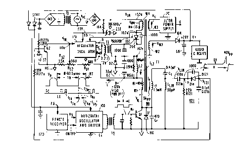
FIGURE 1 illustrates a portion of a television
receiver incorporating a bridge rectifier 101 that
rectifies a mains supply voltage VAC to produce a DC,
unregulated voltage V~. An output stage, or switch
regulator 102, that includes a silicon controlled rectifier
(SCR) switch, referred to herein as SCR 200, produces a
regulated voltage B+ that is coupled to a winding W1 of a
flyback transformer T1. An input terminal 102a of
regulator 102 is coupled to unregulated voltage V~.
Regulated voltage B+ is developed at an output terminal
102d of switch regulator 102. Winding W1 of transformer T1
is coupled to the collector electrode of a deflection
switching transistor Q1 of a horizontal circuit output
stage 99 operating at a horizontal rate fH. A control
signal Hr, at the horizontal rate fH, is developed at the
base of transistor Q1, during a power-up operation. Signal
Hr is applied from a control circuit, referred to herein as
a horizontal oscillator and driver 100, that is coupled to
the base electrode of transistor Q1. Signal Hr controls
the switching of transistor Q1 for generating a deflection
current iy in a series arrangement of a deflection winding
LY, a trace capacitor ct and a linearity inductor LLIN of
horizontal output stage 99. A retrace voltage Vw2 is
produced in a conventional manner across a secondary
winding W2 of transformer T1 in each retrace interval of
each horizontal period H. Each retrace interval occurs
immediately after transistor Q1 becomes nonconductive. A
' DC, run-mode supply voltage V+, that is, illustratively,
200190
-8- RCA 85,154
+26 volts, is produced by rectifying voltage Vw2 in a
rectifier arrangement 104 that is coupled to winding W2.
Voltage V+ is coupled to various circuits of the receiver,
not shown, to provide them with a run supply voltage during
power-up operation.
Voltage B+ is coupled via a voltage divider,
including resistors Rsl, Rs2 and Rs3, to a control circuit
110, that is also referred to herein as regulator
oscillator 110, that is energized during both power-up and
power-off operations to provide a feedback voltage VIN at a
terminal 110a. During power-up operation, control circuit
110 generates a signal Sc at the horizontal rate fH and at
a controllable phase that controls the instant, in each
horizontal interval H, in which SCR 200 becomes conductive.
The phase of signal SC varies in accordance with a
difference between voltage VIN, that is proportional to
voltage B+, and a reference voltage, not shown in FIGURE 1,
that is produced in control circuit 110. The regulation
provided by signal Sc causes regulated voltage B+ to be at
a predetermined DC voltage level such as, illustratively,
+129 volts, during power-up operation.
The anode of SCR 200 is coupled to unregulated
voltage V~ via a winding W4 of transformer T1 . The
cathode of SCR 200 is coupled to an end terminal 102c of a
filter inductor L2. Output terminal 102d, the other end
terminal of inductor L2, where regulated voltage B+ is
developed, is coupled to winding W1 of flyback transformer
T1. A filter capacitor C2 is coupled to output terminal
102d. Signal Sc is coupled via a driver transformer T2 to
the gate electrode of SCR 200.
When a leading edge LE of signal Sc of FIGURE 1,
having a controllable phase as shown in the waveform of
FIGURE 1, occurs, SCR 200 is triggered and becomes
immediately conductive. During normal power-up operation,
leading edge LE occurs at a time tla during a trace
interval of each period H of a voltage VW4 that is
developed across winding W4. During the interval in which
SCR 200 is conductive, a current iL2 in inductor L2, that
200190'
-9- RCA 85,154
charge capacitor C2, increases. The rate of increase of
current iL2 is determined by unregulated voltage V~ and by
regulated voltage B+.
At the end of horizontal trace, a time t2a, shown
in the waveform of FIGURE 1, a retrace pulse portion of
voltage VW4 is developed. Voltage VW4 is developed by
transformer action from voltage VR in retrace capacitor Cr.
Retrace pulse VW4 in winding W4 is poled in such a manner
as to tend to reverse bias SCR 200 and to reduce the
corresponding currents flowing in inductor L2. As a result
of the negative rate of change of current iL2 in inductor
L2, a voltage developed at end terminal 102c is decreased
until a time t3a of retrace pulse portion RT when a catch
diode D2, that is coupled to end terminal 102c, becomes
conductive. The operation of a diode, such as catch diode
D2, is described in detail in U.S. Patent No. 4,163,926,
entitled SWITCH REGULATOR FOR A TELEVISION APPARATUS, in
the name of D.H. Willis.
FIGURE 2 illustrates a detailed schematic diagram
of regulator oscillator or SCR control circuit 110 of
FIGURE 1. Similar numerals and symbols in FIGURES 1 and 2
indicate similar items or functions. During normal power-up
operation, control circuit or regulator oscillator 110 of
FIGURE 2 is synchronized by a retrace signal 49 developed
at input terminal 102a of SCR 200 of FIGURE 1 from voltage
VW4. During shut-down or power-off operation, regulator
oscillator 110 operates continuously as a free running
oscillator and generates signal Sc, as described later on.
Both PNP transistor 53 of FIGURE 2 and NPN
transistor 52 switch states at a rate established by trip
level voltages for a control terminal 54. Control terminal
54 is coupled to the emitter of transistor 52 through a
diode 59. A charging capacitor 55, that is coupled to a
regulated +33 volt source, is charged through a
controllable current source 56 comprising an NPN transistor
57 and a resistor 58, coupled in series. The junction of
the capacitor 55 and the collector of transistor 57 form
control terminal 54 that was mentioned before. The +33 volt
200190
-10- RCA 85,154
source is produced across a zener diode Z33 (shown in Fig.
1) during both power-up and power-off operation.
Complementary transistors 52 and 53 are coupled
together in a latching arrangement. That is, the collector
output terminal of transistor 53 is coupled to the base
input terminal of transistor 52, and the collector output
terminal of transistor 52 is coupled to the base input
terminal of transistor 53, both transistors thereby forming
a regenerative latch.
Under continuous free-running oscillator
conditions of regulator oscillator 110, that occur during
power-off operation, as explained later on, when transistor
52 becomes conductive, current is drawn from the +33 volt
source to the collector of transistor 52 through resistors
60 and 61, thereby turning on transistor 53. Part of the
collector current of transistor 53 is then coupled to the
base of transistor 52 through a resistor 62, thereby
regeneratively turning on both transistors into saturated
conduction. Similarly, when transistor 52 becomes
nonconductive, both transistors regeneratively turn off.
Operation of regulator oscillator 110 for one
free-runing cycle will now be described. Consider an
interval during which transistors 52 and 53 are
nonconducting. The voltage at the base of the transistor 52
is determined by the resistance values of a voltage divider
comprising resistor 63 in series with the parallel
combination of resistors 64 and 62. In order for
transistor 52 to become conductive, voltage V54 must
decrease below a lower trip voltage VL, which is two diode
drops below the voltage at the base of transistor 52.
Should voltage V54 at terminal 54 decrease below level VL,
transistors 52 and 53 would regeneratively turn on.
When both transistors 52 and 53 are conductive,
the voltage divider ratio changes. With transistor 53 in
saturated conduction, resistor 63, rather than resistor 64,
is now effectively paralleled by resistor 62, developing a
new, more positive base voltage for transistor 52, and
establishing an upper level trip voltage VH for control
200190'
-11- RCA 85,154
terminal 54. Should voltage V54 at terminal 54 increase
above level VH, transistors 52 and 53 would regeneratively
turn off.
FIGURES 4a and 4b illustrate idealized waveforms
for voltage V54 at control terminal 54 and the collector
voltage of oscillator transistor 53 during continuous
free-running operation of regulator oscillator 110 that
occurs during power-off operation of the power supply.
During power-off operation, regulator oscillator 110 of
FIGURE 1 is energized but horizontal output stage 99 is
disabled. Consider voltage V54 of FIGURE 2 during the
interval, beginning somewhat after time T1. Transistors 52
and 53 are turned off, and capacitor 55 is charging from
the +33 volt source at a constant rate determined by the
base voltage of transitor 57 of controllable current source
56. The voltage at terminal 54 is thus a decreasing
sawtooth. At time T2, voltage V54 has decreased to its
lower trip voltage level VL, causing transistors 52 and 53
to regeneratively turn on.
The collector of transistor 53 is coupled to one
of output terminals B-B through a diode 65. A primary
winding T2a of transformer T2 of FIGURE 1 is coupled
between terminals B-B. A discharge path of capacitor 55
comprises the terminal of capacitor 55 coupled to the +33
volt source, the emitter-collector path of transistor 53,
diode 65, winding T2a coupled across terminals B-B, and the
other terminal of capacitor 55. To prevent current source
56 from undesirably charging capacitor 55 during the
capacitor discharging interval, the collector of transistor
53 is coupled to the emitter of transistor 57 through a
resistor 77. When transistor 53 conducts, transistor 57 is
cut off, disabling current source 56 during the discharge
interval.
As illustrated in FIGURE 4a, beginning at time
T2, voltage V54 at terminal 54 comprises an increasing
sawtooth. At time T3, voltage V54 has increased to its
upper trip voltage level VH. Transistors 52 and 53
200190"
-12- RCA 85,154
regeneratively turn-off, and the next charging cycle
begins.
As represented by the collector voltage of
transistor 53, illustrated in FIGURE 4b, during the
approximate interval T2-T3, an output signal is coupled to
regulator oscilator 110 output terminals B-B to provide
gating current to turn-on the regulator SCR 200 of FIGURE
1. The actual time width of interval T2-T3 of FIGURES 4a-4b
is relatively unimportant provided sufficient SCR gating
current of a sufficient duration is coupled to SRC 200 of
FIGURE 1 to turn it on.
In normal power-up operation, regulator
oscillator 110 is not left continuously free-running as in
power-off operation but is synchronized with horizontal
deflection. The charging rate of capacitor 55 of FIGURE 2
is varied depending upon the magnitude of the feedback
voltage Vf coupled to a feedback terminal 101 for varying
the turn-on instant and conduction angle of SCR 200 of
FIGURE 1.
FIGURES 3a-3d illustrate waveforms useful for
explaining normal power-up operation of control circuit 110
of FIGURES 1 and 2. Similar numerals and symbols in FIGURES
1, 2 and 3a-3d indicate similar items or functions.
At the beginning of the retrace interval at time
tl of FIGURES 3a, negative going retrace pulse 49 of FIGURE
2 is coupled from input terminal 102a to the base electrode
of transistor 53 through a resistor 149 and a capacitor 150
that causes transistor 53 to become conductive. Therefore,
capacitor 55 becomes immediately afterward substantially
discharged.
After time t2, the beginning of trace, capacitor
55 begins to charge at a rate determined by the voltage at
the base of transistor 57 of current source 56. Voltage V54
decreases until lower trip voltage VL is reached at time
t4. At time t4, the oscillator transistors regeneratively
turn on, resulting in a gating signal S being generated
c(2 )
and coupled to SCR 200 to turn on the SCR, as illustrated
in FIGURE 3c.
200190'
-13- RCA 85,154
Regulator oscillator 110 then continues in a
free-running mode and, as illustrated in FIGURE 3d, several
charge-discharge cycles may occur before another
synchronizing retrace pulse 49 is coupled to terminal 102a
at time t5. In this way, the free-running mode, unlike in
the power-off operation, is interrupted by synchronizing
retrace pulse 49. Thus, as illustrated in FIGURE 3c, in the
subsequent free-running mode after time t4, and prior to
the next retrace pulse 49, another SCR 200 gating signal Sc
may be coupled to the SCR. The number of additional gating
signals will depend upon such factors as the position of
the turn-on instant t4 within the horizontal trace interval
and the charging and discharging rates established for
capacitor 55. Such additional turn-on gating signals are of
relatively little consequence, since the SCR remains in a
conductive state as long as the current through the SCR is
above its holding current level.
To provide regulation, the turn-on instant t4 is
varied within the trace interval by varying the charge rate
of capacitor 55 through a varying voltage at the base of
transistor 57. Transistor 57 base voltage is the
proportioned value of feedback voltage Vf coupled to the
base of transistor 57 through a voltage divider comprising
resistors 70 and 71.
An error amplifying transistor 43 has a base
electrode that is coupled to feedback signal VIN that is
representative of voltage B+ via an input resistor 43a.
Collector load resistors 43b, 70 and 71 form a load
resistance at the collector of transistor 43. A zener diode
Z43 that is coupled to the emitter of transistor 43
determines the threshold voltage of the inverting amplifier
that includes transistor 43. Amplified error voltage Vf
that is developed at a terminal 91, at the collector of
transistor 43, is coupled to the base electrode of
transistor 57.
After time t2, the beginning of trace, capacitor
55 begins to charge at a rate determined by the voltage at
the base of transistor 57 of current source 56. The voltage
-- ~ 2001901
-14- RCA 85,154
V54 decreases until the lower trip voltage VL is reached at time
t4. At time t4, the oscillator transistors regeneratively turn on,
resulting in gating signal Sc(2) being coupled to SCR 200 to turn
the SCR on, as illustrated in FIGURE 3c.
Should the regulated B+ voltage at terminal 102d of
FIGURE 1 decrease, for example, the inverted feedback voltage V f
of FIGURE 2 increases causing the base voltage of transistor 57 to
also increase. The current magnitude of current source 56
increases, increasing the charge rate of capacitor 55. As illustrated
1 0 in FIGURES 3d and 3c by the dotted waveforms V54 and Sc( 1 ), the
lower trip voltage level VL is reached at an earlier instant t3,
generating a gating pulse Sc( 1 ) at the earlier instant t3, as
required for proper regulation.
A user initiated command to enable shutdown or
power-off operation of the television receiver causes remote
receiver 120 of FIGURE 1 to generate an on/off control signal
ON/OFF at an "OFF" state that is applied to driver 100. After
power-off command occurs, the operation of signal on/off causes
switching signal Hr at the base electrode of transistor Q1 to be
2 0 removed. Therefore, output stage 99 is disabled and supply
voltage V+ is not generated. Also, retrace pulse VW4 in winding
W 4 of transformer T1 is not generated. Consequently, retrace
pulse 49 that, in normal power-up operation, synchronizes
regulator oscillator 110 is not generated during the power-off
2 5 operation that follows. Because regulator oscillator 110 is
energized from voltage VUR also during the power-off operation,
regulator oscillator 110 free runs continuously, as described
before.
Assume that, in a given interval that occurs during
3 0 the power-off operation, the magnitude of the anode-to-cathode
voltage of SCR 200 is smaller that the minimum required for
enabling latching operation in SCR 200. In this case, any trigger
pulse of free running control signal Sc that occurs when the anode-
to-cathode voltage of SCR 200 is insufficiently large to enable
200190
-15- RCA 85,154
latching operation in SCR 200, will, nevertheless, cause
SCR 200 to turn on in an unlatched mode. In each such
period of signal Sc, SCR 200 will be turned on for an
interval that is proportional to the pulse width of the
trigger pulse or, for example, to interval T2-T3 of FIGURE
4b. The pulse width of each trigger pulse is constant. It
follows that for a given anode-to-cathode voltage
difference in SCR 200 of FIGURE 1, operating in the
turned-on unlatched operation, the average value of current
1SCR200 through SCR 200 is directly related to the
frequency of the trigger pulses.
Further assume that, in the aforementioned given
interval during the power-off operation, the free running
frequency of the trigger pulses is so low that the average
value of current iSCR200 in SCR 200 in each period of the
trigger pulses is smaller than a load current iL in
resistor RS1. Additionally, assume that the load current iL
is supplied entirely through SCR 200. Therefore, filter
capacitor C2 would discharge by load current iL until
attaining a voltage level that produces a sufficiently
Large anode-to-cathode voltage difference in SCR 200, such
as 10 volts, for enabling the latching operation.
Thereafter, SCR 200 will be triggered by the next trigger
pulse produced by free running oscillator lI0 and the
latching operation will occur in SCR 200.
Because load current iL is small, the discharge
interval for obtaining such sufficiently Large
anode-to-cathode voltage difference that enables the
latching operation in SRC 200 may be equal to, for example,
160 milliseconds. Since retrace pulses VW4 are not present
during the power-off operation, such latching operation
will continue until filter capacitor C2 is again charged to
a voltage that is equal to or greater from unregulated
supply voltage V~, causing the SCR 200 to turn off. At the
end of each such latching operation, the anode-to-cathode
voltage of SCR 200 is again insufficiently large to permit
the next latching operation until the next interval of 160
milliseconds has elapsed.
200190'
-16- RCA 85,154
The latching operation might produce a high
amplitude, wide pulse of current iSCR200 flowing in SCR 200
and in filter inductor L2 that is repetitive at a
corresponding frequency of approximately 6Hz. Such wide
S current pulses might produce an objectionable sound during
power-off operation. The objectionable sound might be
produced due to possible parasitic mechanical vibrations as
a result of the wide pulses current in, for example,
inductor L2. Such sound may be objectionable if it occurs
during the power-off operation when the user does not
expect any sound to come from the turned-off television
receiver. Therefore, it may be desirable to prevent filter
capacitor C2 from being discharged to a level that enables
the undesirable latching operation in the SCR 200, during
the power-off operation.
In accordance with an aspect of the invention, a
signal V121 that is derived from a voltage VLIN developed
in linearity inductance LLIN of FIGURE 1 is applied to a
transistor Q2, operating as a switch, that is coupled to
terminal 110a of regulator oscillator 110. Conduction of
transistor Q2 causes voltage VIN to be zero, which
increases the frequency of signal Sc, during the power-off
operation, to the maximum value, in a manner that is
described Iater on.
The absence of signal V121 causes the free
running frequency of signal Sc to increase in order to
increase the frequency of the trigger pulses to enable
replenishing, during each trigger pulse, of alI the charge
in filter capacitor C2 that was lost during the interval
that elapsed from the immediately preceding trigger pulse
of signal Sc. Because all the charge Lost is replenished
during each period of the trigger pulses, voltage B+ in
filter capacitor C2 will be maintained substantially at the
same level at the end of each trigger pulse. Such level of
voltage B+ is sufficiently high to maintain the
anode-to-cathode voltage of SCR 200 sufficiently low for
preventing the latching operation of the SCR switch from
occurring throughout the power-off operation. The result
~00190~
-1~- RCA 85,154
is that, advantageously, the aforementioned objectionable
sound is eliminated, as explained in detail in U.S. Patent
4,866,525 entitled, A Television Apparatus Power Supply
issued 12 September 1989 to Rodriguez-Cavazos et al.
During power-up operation, signal V121 causes
transistor Q2 to be non-conductive, so as to have no effect
on the switching of the SCR 200. On the other hand, during
the power-off operation, the absence of signal 0121 causes
transistor Q2 to conduct, which increases the frequency of
signal Sc and, in turn, the conduction of SCR 200. The way
signal 0121 is produced and utilized is further explained
below.
During normal power-up operation, AC voltage VLIN
at the frequency fH is developed in linearity inductor
LLIN' A capacitor C121a and a resistor 8121 form a series
arrangment that is coupled in parallel with inductor LLIN
and that dampens ringing in inductor LLIN' During a portion
of retrace, capacitor C121a is charged by a positive going
retrace pulse of voltage VLIN' At the end of such retrace
pulse portion, as the retrace pulse of voltage VLIN becomes
smaller, capacitor C121a, that is already charged, produces
a negative pulse voltage of a bipolar signal U121a at a
cathode of a diode D121 that is coupled between resistor
8121 and capacitor C121a. Diode D121 and a filter capacitor
C121b form a negative peak detector 121 that prqduces
signal V121' The loading effect of detector 121 on inductor
LLIN' is, advantageously, substantially insignificant.
Therefore, detector 121 substantially does not affect
deflection current. Signal V121' that is negative during
power-up operation, is produced at the anode of diode D121
and is coupled through a resistor R122a to the base of
transistor Q2. A protection diode D122 coupled between the
base and the emitter electrodes of transistor Q2 prevents
the base-emitter reverse voltage in transistor Q2 from
exceeding the forward voltage of diode D122.
In accordance with a feature of the invention,
negative signal V121 causes transistor Q2 to be
nonconductive throughout normal power-up operation. On the
RCA 85,154
other hand, throughout power-off operation, negative signal
V121 is not generated and a resistor R122b that is coupled
between the +33 volt supply and the base of transistor Q2
causes transistor Q2 to be conductive. Transistor Q2 of
FIGURE 1 operates as a conductive switch throughout the
power-off operation and as a nonconductive switch
throughout the normal power-up operation. The collector of
transistor Q2 is coupled to input terminal 110a of control
circuit 110 where voltage VIN is developed and causes
voltage VIN to be zero during power-off operation.
Therefore, the rate of change of voltage V54 of FIGURE 2
becomes substantially higher than if voltage B+ were
permitted to control the level of voltage VIN during the
power-off operation. The result is that control circuit lI0
will produce signal Sc of FIGURE 1 at a free-running
frequency that is at the maximum. Therefore, as explained
before, the aforementioned objectionable sound is
eliminated. Had voltage B+ been permitted to control the
level of voltage VIN during the power-off operation, the
frequency of signal Sc might have been at a minimum during
at least a portion of each of the aforementioned 160
milisecond intervals.
Regulator oscillator 110, transistor Q2,
linearity inductance LLIN' switch regulator 102 and
linearity inductor LLIN are each referenced to a common
ground conductor HG that is conductively coupled to mains
supply voltage VAC and that is referred to herein as hot
ground conductor HG. On the other hand, each of remote
receiver 120 and horizontal oscillator and driver 100 of
the television receiver is referenced to a common ground
conductor CG that is conductively isolated from hot ground
conductor HG and that is referred to herein as cold ground
conductor CG. The conductive isolation between the hot and
the cold ground conductors is accomplished, in part, by
energizing remote receiver 120 and driver 100 from a
voltage 78 produced in a conventional manner that is
conductively isolated from hot ground conductor HG. Voltage
~00190'~
-19- RCA 85,154
78 is produced during both the power-off and the power-up
operations.
In accordance with another aspect of the
invention, signal V121 that is applied to regulator
oscillator 110 and to regulator switch 102 through
transistor Q2 is generated from voltage VLIN developed
across inductor LLIN via a signal path that is referenced
to hot ground conductor HG. The signal path includes
capacitor C121a and detector 121 that are, each
conductively coupled to hot ground conductor HG. Signal
V121 that is referenced to hot ground conductor HG has two
levels that correspond to the "OFF" state and to an "ON"
state, respectively, of on/off control signal ON/OFF that
is referenced to cold ground conductor CG. The "power-up"
state of signal V121 is obtained from horizontal rate
signal Hr that is generated only during the power-up
operation. Signal Hr is a transformer coupled signal that
is coupled across the hot-cold barrier formed by
transformer T3. In this way, advantageously, on/off
control signal ON/OFF is applied to transistor Q2 via
transformer T3 that maintains the hot-cold barrier.
Transformer T3 is the same transformer used for supplying
signal Hr to deflection switch transistor Ql, as described
before. Consequently, the need for an additional circuit
element for applying the two states of on/off control
signal ON/OFF across such hot-cold barrier is obviated.
Advantageously, extracting the on/off information from
voltage VLIN is accomplished without adversely affecting
deflection current i
Y.