Note: Descriptions are shown in the official language in which they were submitted.
20 023 82
CLOCK ADAPTER USING A PHASE LOCKED LOOP
CONFIGURED AS A FREQUENCY MULTIPLIER WITH
A NON-INTEGER FEEDBACK DIVIDER
Field of the Invention
This invention relates to a phase locked loop
configured as a frequency multiplier, which utilizes a
controlled commutator to achieve frequency translation in
the feedback path, to achieve a non-integer divide ratio,
and thereby produce an output that is not an integer
multiple of the reference input. A preferred embodiment
discloses a circuit that directly translates a 2.048 MHz
clock to a 1.544 MHz clock and vice versa.
Description of the Related Technology
The use of a phase locked loop as a frequency
multiplier is well documented in the literature. The
conventional implementation of such a circuit introduces
a digital divider into the feedback path of the loop. In
this way the output of the VCO is divided by an integer N
before it is compared to the reference input by the phase
comparator. In order for the loop to lock, both the
reference input and the divided VCO output must be
identical in both phase and frequency. To achieve this,
the loop must maintain the output of the VCO at a
frequency that is N times greater than that of the
reference input. Since a digital divider is limited to
division by an integer, a frequency multiplier which
includes a digital divider can only produce an output
which is an integer multiple of the input reference.
In the field of telephone switching systems, the
primary digital carrier employed in North America consists
of twenty-four channels operating at a 1.544 megabits per
second rate. In the multiplex digital switching systems
used in Europe and in many Private Branch Exchanges (PBX),
32 channels are switched at a 2.048 megabits per second
rate. Equipment that interfaces to both types of systems
has the constant need to convert a 2.048 MHz clock to a
1.544 MHz clock and vice versa. A clock adapter, used for
20 023 82
2
this purpose, must either accept a 2.048 MHz input clock
as its reference and produce a 1.544 MHz output clock, or
accept a 1.544 MHz input clock as its reference and
produce a 2.048 MHz output clock. In both cases the clock
adapter must produce an output that is not an integer
multiple of the reference input. Clearly, a conventional
frequency multiplier will r.~t work in this application and
an alternate solution must be found.
Several devices have been developed to address
the problem of clock conversion, such as disclosed in U.S.
Patent No. 4,154,985, issued to Ernst A. Munter. The
Munter patent discloses a frequency converter circuit
composed of a series connection of a frequency multiplier,
a digital frequency converter and a second frequency
multiplier. In the Munter device the first frequency
multiplier produces an intermediate frequency higher than
the desired output. The digital frequency converter in
turn modifies the period of the intermediate frequency
clock, in intervals established by the period of the
intermediate clock, to produce an intermediate clock that
has the desired frequency. The intermediate clock,
however, contains a large amount of fitter making it
unsuitable for use in the system. A second phase locked
loop, also configured as a frequency multiplier with a
narrow bandwidth loop filter, is used to reduce the fitter
and also produces a "two times" clock output used
elsewhere in the system. Such a solution is costly and
relatively complex since two frequency multipliers are
required.
U.S. Patent No. 4,360,788, issued to Erps et al.,
discloses an implementation which uses only one frequency
multiplier. This embodiment uses a phase locked loop
frequency synthesizer that incorporates a single side band
mixer, a pulse incrementer and a programmable frequency
divider in the feedback path. The single side band mixer
and the pulse incrementer allow the output of the VCO to
be slightly shifted before reaching the programmable
20 023 82
3
divider. In this way non-integer multiples of the
reference frequency can be generated. Such a circuit
could be used to convert a 2.048 MHz clock to a 1.544 MHz
clock and vice versa. For example, if the disclosed
circuit were used to convert a 2.048 MHz clock to a 1.544
MHz clock, the combined effect of the single side band
mixer and the pulse incrementer would be required to
translate the VCO output 504 kHz lower in frequency. This
would allow the loop to maintain the VCO output at the
desired frequency. In this configuration, however, the
accuracy of the output is dependent not only on the input
reference but also on the accuracy of the signal source
used to drive the single side band mixer. The Erps, et
al. solution, therefore, involves a relatively high degree
of complexity and multiple sources of potential error.
U.S. Patent No. 3,516,007, issued to Bos et al.,
discloses a circuit that increases the resolution of the
programmable divider in the feedback path and thereby
allows the frequency multiplier to produce noninteger
multiples of the reference input. By adding and deleting
pulses applied to the programmable divider the time
average frequency of the feedback signal is shifted. In
order to remained locked the VCO output is driven slightly
higher or lower in frequency. Further, by controlling the
feedback signal in this manner the typically stringent
requirements on the loop filter are somewhat reduced.
While this solution is practical for increasing the
resolution by a factor of ten it, becomes difficult to
implement as the degree of resolution increases. In order
to convert 2.048 MHz. to 1.544 MHz the divide ratio
required would be 1.544/2.048 or 0.75390625. The degree
of resolution that would be required to achieve this
division ratio renders the Bos et al. solution
impractical. Even if a practical solution could be found,
the integration time required to achieve a time average
frequency of the feedback signal equal to that of the
20 023 82
4
input signal would once again place severe constraints on
the design of the loop filter.
The concept of modifying the period of the
feedback signal is also presented in U.S. Patent No.
3,516,007. The circuit disclosed in the '007 patent,
however, can only adjust the period of the feedback signal
in intervals defined by the period of the VCO output
clock. The invention disclosed in the present application
is capable of adjusting the period of the feedback signal
in substantially smaller intervals.
In all of the previous designs just discussed,
one common theme can be found. All circuits use a single
phase VCO. Various derivations on how the feedback signal
is generated have been presented but all use one VCO
output.
The present device also includes a controlled
commutator, examples of which can be found in other
references. U.S. Patent 4,584,695 issued to Wong et al.,
clearly describes a multi phase oscillator and a
controlled commutator used to make small adjustments in
the clock used by their system to recover data. In the
Wong et al. disclosure the oscillator and controlled
commutator is operated open loop.
Also relevant is U.S. Patent 4,733,197 issued to
Chow et al. The block diagram of this circuit is somewhat
similar to the present invention. The key differences
include the fact that the Chow et al. VCO has only one
output, the multiple phases used by downstream logic are
generated in a purely digital block, and the commutator is
used to make relatively large phase adjustments in the
feedback signal in order to extend the lock range of the
loop.
Sumraary of the Invention
The present invention is a phase locked loop
frequency multiplier. The particular embodiment disclosed
converts a 2.048 megahertz clock to a 1.544 megahertz
20 023 82
clock or vice versa. Whereas previous frequency
multipliers have been made to multiply by non-integer
values by periodically adjusting the period of the
feedback signal from the VCO, the present invention uses
5 a multiphase VCO and a controlled commutator to adjust the
period of the feedback signal before it is applied to the
feedback divider in steps that are smaller than currently
possible by state of the art means. The various VCO
phases are equally spaced in time. By periodically
switching from one original phase to a phase that either
leads or lags the original phase, the period of the
feedback signal will be either shortened or lengthened,
respectively. If the number of phases are relatively
large and the VCO frequency is relatively high, then the
size of each step will be small. For example, if the VCO
is operating at 1.544 MHz and has 12 phases, then the time
between each phase is 53.97ns. Each adjustment to the
period of the feedback signal would therefore be 53.97ns.
This is a much smaller adjustment than the 647.67ns
adjustment which is the smallest adjustment possible when
each adjustment step is defined by the period of the 1.544
MHz clock. Since the adjustments are relatively small,
the rate at which they occur must be more frequent. The
frequency of the fitter introduced into the feedback
signal will be relatively high and its amplitude will be
relatively small. Both of these conditions simplify the
design of the loop filter needed for fitter suppression.
A preferred embodiment of the present invention operates
the VCO at a multiple of the desired output, thus further
reducing the time between each phase. Subsequently, the
output of the VCO must be divided to derive the desired
output.
Brief Description of the Drawings
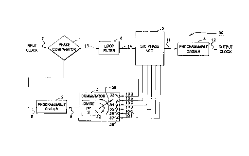
Fig. 1 is a system block diagram of the present
invention;
._ Zp 023 82
6
Fig. 2 is a circuit diagram of Multi-phase VCO as
depicted in Fig. 1;
Fig. 3 depicts the phase relationships in the
ring oscillator and commutator circuits as shown in Fig.
1.
Fig. 4 depicts the phase relationships in the
commutator during an increment operation.
Fig. 5 depicts the phase relationships in the
commutator during a decrement operation.
Fig. 6 is a circuit diagram of the commutator as
depicted in Fig. 1.
Description of the Preferred Embodiment
A block diagram of a preferred embodiment is
shown in Fig. 1. This configuration is basically that of
a frequency multiplier except that: 1) the VCO 5 has
multiple output phases, 2) a commutator 3 is placed
between the VCO 5 and the programmable divider 2 in the
feedback loop and 3) a programmable divider 4 is added to
derive the output clock 12 from the output 11 of the VCO.
Since the functioning of a phase comparator, loop filter
and programmable dividers are well known, only the multi-
phase VCO, controlled commutator and the general operating
modes will be explained in detail.
Multi-Phase VCO
As seen in Fig. 2, the voltage controlled
oscillator 5 used in a preferred embodiment is implemented
as a three stage ring oscillator. Each of the three
stages are composed of an inverter 18, 19, 20 and a
capacitor 21, 22, 23. The inverters are connected in a
ring and a capacitor is connected to each of the nodes 24,
25, 26 between the invertors. The rate at which an
invertor can charge or discharge a capacitor is controlled
by a common current reference. The frequency of
oscillation can be controlled by varying this reference
current. A voltage to current converter 27, provides the
X002382
7
means by which the error voltage 14, generated by the
phase comparator 1 and the loop filter 6, controls the
reference current. The output of each stage in the ring
is buffered with an inverting buffer 28, 29, 30. The
oscillator is designed such that the output 15, 16, 17 of
each stage will have a 50~s duty cycle and each oscillator
phase will be equally spaced in time, as shown in Fig. 3.
These phases, in turn, drive simple combinational logic
that produces the six phases 10a, lOb, lOc, lOd, 10e, lOf
used by the controlled commutator 3. The Multi-Phase VCO
5 also includes a divide by two circuit 31 that produces
a 50~ duty cycle output clock 11 which is used to generate
the output clock 12.
Controlled Commutator
Each of the six phases 10a, lOb, lOc, lOd, 10e,
lOf has a duty cycle of 33~s and the falling edges 40, 41,
42, 43, 44, 45 are equally spaced in time, as shown in
Fig. 3. By switching from one phase to an adjacent phase,
small periods of time can be added or subtracted from the
period of the output signal. To fully appreciate this,
assume that the commutator 3 is set to select signal lOc.
In this position signal lOc is passed to divide by two
circuit 32 to produce signal 9 which has a 50~ duty cycle
at half the frequency of signal lOC. If the commutator is
incremented from signal lOc to lOd on the falling edge 46
of signal lOc then the period of signal 9 will be
shortened by one sixth of the period of the VCO signal
lOc, as shown in Fig. 4. Likewise, if the commutator 3 is
set to select signal lOc and is decremented to lOb after
the falling edges 47, 48 of both lOc and lOb then the
period of signal 9 will be lengthened by one sixth of the
period of lOc, as shown in Fig. 5. In the case of either
adjustment the duty cycle of the commutator output 9
varies from 50~ by less than 10~s.
Since the period of signal 9 can be modified in
this manner it is possible to change the time average
20 023 82
8
frequency of signal 9 by periodically adding or
subtracting a small time increment to or from signal 9.
The regularity with which this is done determines the
amount of frequency shift induced into signal 9. As will
be described, the commutator 3 is controlled by a simple
divide by sixteen circuit. This circuit causes the
commutator 3 to switch phases once every sixteen counts.
The clock used by this circuit is different for each mode
of operation.
The actual implementation of the Controlled
Commutator 3 is best understood by referring to Figure 6.
Each of the "poles" 33, 34, 35, 36, 37 and 38 of the
commutator are electrically connected to one terminal of
AND gates 33a, 34a, 35a, 36a, 37a and 38a shown in the
block diagram. The "wiper" 39 is analogous to the output
70 of OR gate 39a. The divide by two function 32 is
performed by the TFF block 32a. The selection means
(normally achieved by the physical movement of the wiper
39) is accomplished by the 1 of 6 decoder 49 and the state
counter 55. Together these two blocks generate the enable
signals which drive the second input of AND gates 33a,
34a, 35a, 36a, 37a and 38a.
For example a high on signal 59c would permit
signal lOc to pass through to OR gate 39a along signal
path 62c. In this case the output 70 of OR gate 39a is
virtually identical to signal lOc. The commutator output'
9 is then generated by dividing signal 39a by 2 in TFF
32a.a If a "speed up" request is received on signal path
64, the state counter 55 is incremented causing enable 59c
to return low and enable signal 59d to go high. This
advances the phase of the commutator output 9 from lOc to
lOd. The "speed up" operation is shown in FIGURE 4. On
the other hand, if a "slow down" request is received on
signal path 65, the state counter 55 is decremented
causing enable 59c to return low and enable signal 59b to
go high. This allows the phase of the commutator output
9 to fall back from that of lOc to match that of lOb. The
2002382
9
"slow down" operation is shown in FIGURE 5. As will be
readily appreciated by those skilled in the art, any
conventional implementation of a controlled commutator may
be utilized, such as those already referenced in U.S.
Patent Numbers 4,584,695 and 4,733,197.
General Modes of Operation
A preferred embodiment has two modes of
operation. The first mode accepts an input clock at 2.048
MHz and produces an output clock at 1.544 MHz. The second
mode of operation accepts an input clock at 1.544 MHz and
produces an output clock at 2.048 MHz. Both modes will be
discussed in detail and will refer to the system block
diagram in Fig. 1. Both modes operate the VCO 5 at a
frequency that is less than eight times the reference
input. This greatly eases the design requirements for the
loop filter as well as the overall design of the phase
locked loop.
One novel aspect of the present invention is that
through the combination of the multi-phases VCO 5 and the
controlled commutator 3, relatively tiny adjustments can
be made to the feedback signal 13. By keeping the
feedback signal 13 frequency adjustments small the loop
will experience only minor disruptions. Further by
adjusting the period of the feedback signal 13 in small
increments and by making these adjustments at a high rate,
the frequency content of the disruption is kept high.
These high frequency components can subsequently be
removed or greatly reduced by the loop filter 6. The
result is a low fitter output with an accuracy derived
from the input reference 7.
2.048 MHz to 1.544 MHz Conversion
In this mode of operation a 2.048 MHz clock
signal is applied to input lead 7. The programmable
divider 2 in the feedback path is set to divide by three,
the programmable divider 4 in the output path is set to
Zp 023 82
divide by four and the desired output is 1.544 MHz. Given
this set of conditions the operating conditions for each
block in Fig. 1 can be determined. If the output of the
programmable divider 4 in the output path is to be held at
5 1.544 MHz and this divider is set to divide by four then
VCO output 11 must be held at 6 . 176 MHz . Therefore the
VCO 5 must be operating at 12.352 MHz. The period of each
of the six VCO phases (l0a-10f) would then be 80.959ns and
the time between adjacent phases is 13.493ns. If the
10 commutator 3 were not switched and selected only one VCO
phase then the frequency of signal 9 would also be 6.176
MHz.
In order for the loop to lock, the signal applied
to the second phase comparator input 8 must have the same
frequency and phase as the signal applied to the input
lead 7. As previously stated a 2.048 MHz clock is applied
to lead 7 so the frequency of signal 8 must also be 2.048
MHz. Since the programmable divider 2 in the feedback
path is set to divide by three the output of the
commutator, signal 9, must be maintained at 6.144 MHz.
Therefore, it is desirable to periodically add small time
increments to the period of signal 9 such that the time
average frequency of this signal will be translated from
6.176 MHz to 6.144 MHz.
To understand this translation, one need to look
at the relationship between a 6.176 MHz clock and the
desired 6.144 MHz clock. If one starts at a point in time
when the rising edge of both clocks exactly align, one
observes that the edges diverge until they are 180 degrees
out of phase and then converge again. The edges will
realign 31.25usec later. During this time the 6.144 MHz
clock will have counted 192 cycles and the 6.176 MHz clock
will have counted 193 cycles. Since the goal is to
translate the 6.176 MHz clock to a 6.144 MHz clock, there
is a need to remove one cycle of the 6.176 MHz clock
during this 31.25~sec period. One cycle of the 6.176 MHz
clock has a period of 161.92ns which is 12 times the time
..~. 20p~3s2
11
interval between VCO phases . Therefore, if the commutator
3 is decremented twelve times during the 31.25usec
interval then the time average frequency of commutator
output signal 9 will be 6.144 MHz. In order'to minimize
fitter these decrements should be equally spaced in time.
Since the commutator output 9 is required to make 192
cycles during the 31.25usec interval, the twelve
decrements may be equally spaced by initiating one
decrement for every 16 cycles of the commutator output 9.
In a preferred embodiment this control function is
performed by a divide by 16 circuit.
1.544 MHz to 2.048 MHz Conversion
In this mode of operation a 1.544 MHz clock is
applied to input lead 7. The programmable divider 2 in
the feedback path is set to divide by four, the
programmable divider 4 in the output path is set to divide
by three, and the desired output frequency is 2.048 MHz.
Again the operating conditions for each circuit block in
Fig. 1 can be determined. Since the output of the
programmable divider 4 in the output path 11 is to be held
at 2.048 MHz and the divider 4 is set to divide by three,
the VCO output 11 must be held at 6.144 MHz. The VCO 5
must operate at 12.288 MHz. The period of each of the six
VCO phases (l0a-lOf) is 81.380nsec and the time between
adjacent phases is 13.563ns. If the commutator 3 were to
remain on one particular VCO phase then the frequency of
signal 9 would also be 6.144 MHz. The programmable
divider 2 in the feedback path is set to divide by four
such that the output signal 9 of the commutator signal 9
must be maintained at 6.176 MHz in order for the loop to
lock. It is therefore desirable to periodically subtract
small time increments from the period of signal 9 such
that the time average frequency will be 6.176~MHz.
As was presented for the case of conversion from
2.048 MHz to 1.544 MHz, the two frequencies of interest
are 6.144 MHz and 6.176 MHz. In this case, however, one
m~. 2~ 023 s2
12
cycle must be added to the 6.144 MHz signal during a
31.25usec interval in order to achieve the desired 6.176
MHz signal. The total amount of time that must be
subtracted from the 6.144 MHz clock in order to add one
cycle is 162.76ns. Again this is twelve times the time
interval between VCO phases. Therefore, if the commutator
3 is incremented twelve times during the 31.25usec
interval then the time average frequency of commutator
output signal 9 will be 6.176 MHz. This can be
accomplished by initiating one increment for every sixteen
cycles of the VCO output 11. In this mode the control
function is performed by the same divide by sixteen
circuit used in the other conversion mode with the clock
being taken from the VCO output 11.