Note: Descriptions are shown in the official language in which they were submitted.
)OZ555
TITLE OF THE INVENTION
Television Receiver
BACKGROUND OF THE INVENTION
Field of the Invention
The present invention relates generally to television
receivers, and more particularly to television receivers
having a still picture reproducing function.
Description of the Background Art
Conventional methods for separating a luminance
~0 signal (Y signal) and a chrominance signal (C signal) from
a composite television signal include a method using a
movement adaptation type YC separating circuit.
Fig. 1 is a block diagram showin~ a construction of a
conventional movement adaptation type YC separating
circuit disclosed in Japanese Patent Laying-Open No.
61-123295. Referring to Fig. 1, a composite video signal
is converted to an 8-bit digital signal by an A/D
converter 1. This digital signal is delayed by lH (H
being a horizontal sync signal period) in a line memory 2
and it is further delayed by 524H~s in a frame memory 3.
Input and output signals of the line memory 2 supplied to
a subtracter 4, where the output signal of the line memory
2 is subtracted from the input signal of the line memory
2. A luminance signal component is offset in the output
2S of the subtracter 4 by line correlation of the composite
, . : . ~ - : ~ : ,
2~;25~i5
television signal. However, since a high frequency
component of the luminance signal in the vertical
direction of the screen remains, this component is removed
by a horizontal bandpass filter 5. The output of the
horizontal bandpass filter 5 is supplied as a first
chrominance signal MC to a mixing circuit 9. The output
signal of the A/D converter 1 and the first chrominance
signal MC are supplied to a subtracter 6, wher~ the first
chrominance signal MC is subtracted from the output signal
lQ of the A/D converter 1. As a result, the chrominance
signal component is offset in the composite television
signal as the output signal of the A/D converter 1,
whereby a first luminance signal MY is obtained. This
first luminance signal MY is supplied to the mixing
circuit 9.
In the meantime, the output signal of the A/D
converter 1 and the output signal of the frame memory 3
are supplied to a subtracter 7, where the output signal of
the frame memory 3 is subtracted from the output signal of
the A/D converter 1. Since the output signal of the frame
memory 3 is a signal delayed exactly by one frame from the
composit2 video signal outputted from the A/D converter 1,
a luminance signal component is offset in the output
signal of the A/D converter 1 by frame correlation so that
a second chrominance signal SC is obtained. This second
.. . . .
` ~ Z~ 55
chrominance signal SC is supplied to the mixing circuit 9.
The output signal of the A/D converter 1 and the second
chrominance signal SC are supplied to a subtracter 8,
where the second chrominance signal SC is subtracted from
the output signal of the A/D converter 1. As a result,
the color signal component is offset in the composite
video signal outputted from the A/D converter 1, whereby a
second luminance signal SY is obtained. The second
luminance signal SY is supplied to the mixing circuit 9.
The output signal of the A/D converter 1 and the
output signal of the frame memory 3 are supplied to a
movement detecting circuit 10. This movement detecting
circuit 10 evaluates a difference signal between frames of
the composite video signal and determines based on the
difference signal whether an image formed by the present
composite video signal is a moving picture or a still
picture. The output of the movement detecting circuit 10
is supplied to the mixing circuit 9. The mixing circuit 9
selects the first luminance signal MY and the first
chrominance signal MC separated by utilizing the line
correlation and outputs those signals as the luminance
signal Y and the chrominance signal C if ~he output of the
movement detecting circuit 10 indicates a moving picture.
On the other hand, if the output of the movement detecting
circuit 10 indicates a still picture, the mixing circuit 9
` - ;20~255~;
selects the second luminance signal SY and ~he second
chrominance signal SC separated by utilizing the frame
correlation and outputs those signals as ~he luminance
signal Y and the chrominance signal C.
The movement detecting circuit 10 may be constructed
to output a detection signal having its level changing in
an analog manner according to the moving condition of the
picture and the mixing circuit 9 may be constructed to mix
the first luminance signal MY and the second luminance
signal SY with a ratio according to the level of ~he
detection outpu~ and to mix the first chrominance signal
MC and the second chrominance signal SC with that ratio.
The above mentioned movement adaptation type YC
separating circuit makes it possible to separate a
luminancé signal and a chrominance signal with high
qualities without causing any mixture or remaining of
those signals.
If still picture reproduction is to be effected in a
television receiver comprising a movement adaptation type
YC separation circuit as described above, still picture
reproduction processing is conventionally carried out by
using a dedicated frame memory. More specifically, a
frame memory other than the frame memory pro~ided in the
movement adaptation type YC separating circuit is provided
to carry out still picture reproduction processing.
_ ~ _
., , ~ , ~ . - . : ,,
2~2555
However, this frame memory dedicated to s~ill picture
reproduction processing is very expensive and the use of
such a dedicated frame memory is disadvantageous in cost.
SI~RY OF THE INVENTION
An object of the present inven~ion is to effect still
picture reproduction with an inexpensive construction in a
television receiver including a movement adaptation type
YC separating circuit.
A television receiver according to the present
invention includes luminance signal/chrominance signal
separating means for separating a luminance signal and a
chrominance signal from a composite video signal. This
luminance signal/chrominance signal separating means
includes delay means, first extracting means, second
extracting means, a movement detecting circuit and a
mixing circuit. The delay means includes a plurality of
delay elements connected in series, which delay the
composite video signal successively and output a plurality
of composite video signals having different prescribed
delay times. The fi.rst extracting means evaluates an
input signal and/or an output signal of the delay means
and extracts a first luminance signal and a second
chrominance signal based on line correlation of the
composite video signal. The second extracting means
evaluates the input signal and/or the output signal of the
-- 5 --
2~
delay means and extracts a second luminance siqnal and a
second chrominance signal based on frame correlation of
the composite video signal. The movement detecting
circuit detects a movement of a picture. The mixing
circuit controls a mixing ratio of the first and second
luminance signals and a mixing ratio of the first and
second chrominance signals in response to the output of
the movement detecting circuit. The television receiver
of the present invention further includes control signal
generating means and switch means. The control signal
generating means generates a control signal in response to
a still picture reproduction instruction. The switch
means is controlled in response to the control signal to
form a circulating circuit which short-circuits the input
and output terminals of the delay means in the still
picture reproduction so that the composite video signal
circulates in the delay means. In the still picture
reproduction, the luminance signal/chrominance signal
separating means separates the luminance signal and the
chrominance signal based on the output obtained from the
circulating circuit.
Thus, according to the present invention, processing
for still picture reproduction is carried out by using the
delay means included in the luminance signal/chrominance
~ Z~
signal separating means (the movement adaptation type YC
separating circuit).
According to the present invention, the delay means
provided in the luminance signal/color signal separating
means is also used for still picture reproduction and
consequently processing for still picture reproduction can
be carried out with an inexpensive construction.
The foregoing and other objects, features, aspects
and advantages of the present invention will become more
apparent from the following detailed description of the
present invention when taken in conjunction with the
accompanying drawings.
BRIEF DESCRIPTION OF THE DRAWINGS
Fig. 1 is a block diagram showing a construction of a
conventional movement adaptation type YC separating
circuit.
Fig. 2 is a block diagram showing construction of an
embodiment of the present invention.
Fig. 3 is a block diagram showing a construction of
another embodiment of the present invention.
Fig. 4 is a block diagram showing a construction of a
further embodiment of the present invention.
DESCRIPTION OF THE PREFERRED EMBODIMENTS
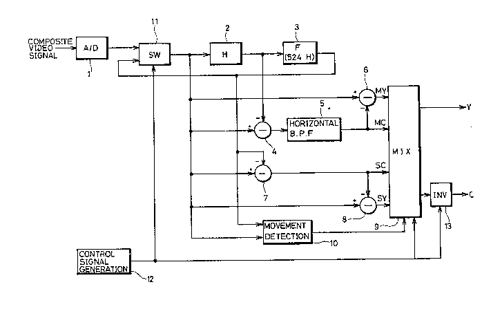
Referring first to Fig. 2, an embodiment of the
present invention will be described. The embodiment shown
- - . .. .
2555
in Fig. ~ has the same construction as that of the
conventional movement adaptation type YC separating
circuit show~ in Fig. 1, except for the below described
features. The portions corresponding to those in Fig. 1
are denoted by the same reference numerals and the
description thereof is not repeated. The embodiment shown
in Fig. 2 further comprises a switch circuit 11, a control
signal generating circuit 12 and a chroma inv~rter circuit
13 in order that the movement adaptation type YC
separating circuit may have a still picture reproducing
function. The swLtch circuit 11 selects either an output
signal of the A/D converter 1 or an output signal of the
frame memory 3 and outputs the selected signal to the line
memory 2. The control signal generating circuit 12
generates a control signal in response to an instruction
of still picture reproduction from a still picture
reproduction switch (not shown) manually operated by the
user for e~ample. The control si~nal is supplied to the
switch circuit 11, the mixing circuit 9 and the chroma
inverter 13. Switching operation of the swi~ch circuit 11
is controlled in response to the control signal. The
. mixing circuit 9 is constructed to select and output the
firs~ luminance signal MY and ~he first chrominance signal
MC in response to the above mentioned control signal. The
chroma inverter circuit 13 is enabled in response to the
-- 8 --
i5
above mentioned control signal to invert the polarity of
the chrominance signal for one frame (525H's) so as to
maintain a sequence of a chrominance subcarrier for two
frames in still picture reproduction.
Next, operation of the embodiment shown in Fig. 2
will be described.
First, in normal reproduction, the control signal
from the control signal generating circuit 12 is at low
(L) level and the switch circuit 11 is at the position
selecting the output signal of the A/D converter 1.
Accordingly, the movement adaptation type YC separating
circuit operates in the same manner as in the conventional
circuit shown in Fig. 1. In this case, the chroma
inverter circuit 13 is disabled and does not operate.
lS Thus, the chroma inverter 13 outputs the chrominance
signal C supplied from the mixing circuit 9 as it is.
Next, when the still picture reproduction switch (not
shown) is pressed, the control signal from the control
signal generating circuit 12 rises to high (H) level.
Consequently, the switch circuit 11 is turned to the
position for selecting the output signal of the frame
memory 3. As a result, the switch circuit 11, the line
memory 2 and the frame memory 3 constitute a circulating
circuit of one frame (525H's).
~, . - , .
;i55
Accordingly, the first and second luminance signals
MY and SY and the first and second chrominance signals MC
and SC supplied to the mixing circuit 9 form a circulation
signal of one frame, namely, a still picture signal.
Since the two signals inputted to the subtracter 7 are the
same, the chrominance signals have the same phase and it
is not possible to separate a luminance signal and a
chrominance signal in a three-dimensional manner by
utilizing frame correlation. Accordingly, i~ is necessary
to separate a luminance signal and a chrominance signal in
a two-dimensional manner by utilizing only line
correlation in a field in still picture reproduction.
Therefore, according to this embodiment, when the con~rol
signal from the control signal generating circuit 12
attains H level, the mixing circuit 9 selects and outputs
only the first luminance signal MY and the first
chrominance signal MC obtained by the forced
two-dimensional processing, independent of the output of
the movement detecting circuit 10.
As to the chrominance signal selected by the mixing
circuit 9, the phase sequence for two frames could not be
maintained without any processing. However, the chroma
inverter circuit 13 is enabled in response to the control
signal of H level, whereby the phase of the chrominance
signal is inverted for each frame by the chroma inverter
-- 10 --
1;25~iiS
circuit 13. As a result, the sequence of the chrominance
signal for two frames can be maintained and a continuous
chrominance subcarrier can be obtained.
The timing of switching between L level and H level
of the control signal from the control signal generating
circuit 12 is selected to be coincident with a vertical
blanking pexiod. Accordingly, the timing of switching of
the switch circuit 11, namely, the timing of generation of
discontinuous points of the phases of the chrominance
subcarrier coincides with the timing of inversion of the
phase by the chroma inverter circuit 13 and thus a perfect
continuity of the chrominance signal can be maintained.
In the above described embodiment, a circulating
circuit of one frame (525H~s) is formed in still picture
reproduction, however, if a circulatin~ circuit of two
frames (1050H's) is formed by additionally providing
another frame memory, a luminance signal and a chrominance
signal can be separated in a three-dimensional manner in
still picture reproduction. In such a case, a still
picture of a higher quality can be obtained because there
are no pxoblems such as cross color or dot interference in
a two-dimensional separation. Further, in such a case,
the chroma inverter circuit 13 needs no~ be provided since
a sequence of the chrominance subcarrier of the two-frame
period can be always maintained. Next, another embodimen~
., . :.: :.,
. . ~ . . .
2~2~i~;5
for still picture reproduction by using a composite video
signal obtained from a circulatinq circuit of two frames
will be described.
In the embodiment shown in Fig. 3, a frame memory 14
is additionally provided betwean the frame memory 3 and
the switch circuit ll. This frame memory 14 is
constructed to delay an input signal by a one-frame period
(525H's). The other construction is the same as that of
the embodiment shown in Fig. 2 and the corxesponding
portions are denoted by the same reference numerals.
According to the embodiment shown in Fig. 3, a circulating
circuit of two frames is formed by the switch circuit 11,
the line memory 2, the frame memory 3 and the frame memory
14 in still picture reproduction. Accordingly, the two
composite video signals inputted to the subtracter 7 in
still picture reproduction have timings different from
each other by one frame and consequently a chrominance
signal can be separated by frame correlation. Similarly,
a luminance signal can be separated in the subtracter 8.
Thus, in the embodiment shown in Fiq. 3, it is possible to
separate a luminance signal and a chrominance signal
two-dimensionally by utili~ing line correlation and to
separate a luminance signal and a color signal
three-dimensionally by utilizing frame correlation.
Accordingly~ e~en in still picture reproduction, the
- 12 -
.. ,. , , ,. ~ - .: ,.. ~ . .. . .... . . .
~ ~ ~2 S ~ 5
mixing circuit 9 is controlled by the output of the
movement detecting circuit 10. More specifically, in
still picture reproduction, the mixing circuit 9 selects
and outputs the first luminance signal MY and the first
chrominance sîgnal MC if there is a movement in the
composite video signals of two frames circulating in the
above mentioned circula-ting circuit, and it selects and
outputs the second luminance signal SY and the second
chrominance signal SC if there is no movement in the
composite video signals. As a result, in the embodiment
shown in Fig. 3, the control signal from the control
signal generating circuit 12 is not applied to the mixing
circuit 9.
Next, still another embodiment for $orming a
circulating circuit of two frames in still picture
xeproduction will be described with reference to Fig. 4.
In the embodiment shown in Fig. 4, the output signal of
the switch circuit 11 is delayed by a one-frame period
(525H's) in the frame memory 15 and then delayed by lH in
the line memory 16, and further delayed by 524H's in the
frame memory 17. The output signal of the frame memory 17
is applied to the switch circuit 11 together with the
output signal of the AJD converter 1. The subtracter 4
separatés a chrominance signal by the inputJoutput signals
of the line memory 16. The subtracter 6 subtracts khe
Z5~5
output signal of the horizontal bandpass filter 5 from the
output signal of the frame memory 15, so as to separate a
luminance signal. The output signal of the switch circuit
11, the output signal of the frame memory 15 and the
output signal of the frame memory 17 are supplied to
coefficient multipliers 18, 19 and 20, respectively. The
coefficient multipliers 18 and 20 multiply the respective
input signals by -1/4 and the coefficient multiplier 19
multiplies the input signal by 1/2. The output signals of
those coefficient multipliers 18, 19 and 20 are supplied
to an adder 21, where those signals are added. The frame
memory 15, the line memory 16, the frame memory 17, the
coefficient multipliers 18 to 20 and the adder 21
constitute a three-dimensional comb filter, which
separates the second chrominance signal SC. The
subtracter 8 subtracts the second chrominance signal SC
from the output signal of the frame memory 15, thereby
obtaining the second luminance signal SY. The other
construction is the same as that of the embodiment shown
in Fig. 2. In the embodiment shown in Fig. 4, a
circulating circuit of two frames is formed by the switch
circuit 11, the frame memory 15, the line memory 16 and
the frame memory 17 in still picture reproduction. In
still picture reproduction~ a luminance signal and a
chrominance signal is two-dimensionally separated and
- 14 -
2~25~5
three-dimensionally separated from the composite video
signal obtained from the circulating circuit.
Consequently, in the embodiment of Fig. 4, similarly to
the embodiment of Fig. 3, the mixing circuit 9 in still
picture reproduction is controlled by the detection signal
from the movement detecting circuit 10 so as to select and
output either the first luminance signal MY, the first
chrominance signal MC or the second luminance signal SY,
the second chrominance signal SC.
According to the embodiment shown in Fig. 3 or Fig.
4, a luminance signal and a chrominance signal can be
separated three-dimensionally by utilizing frame
correlation even in still picture reproduction as
described above and cons~quently a still picture of high
quality can be obtained without any adverse effect such as
cross color or dot interference. In addition, the chroma
inverter circuit 13 used in the embodiment of Fig. 2 needs
not be provided.
Although the present invention has been described and
illustrated in detail, it is clearly understood that the
same is by way of illustration and example only and is not
to be taken by way of limitation, the spirit and scope of
the present invention being limited only by the terms of
the appended claims.
_ 15 -
: : - .: :,, . . . - . ........... .. .. . .
.. -. ~. . . ~ . .. :. ,. : .