Note: Descriptions are shown in the official language in which they were submitted.
2~)3159
INTERFEROMETRIC IMAGING SYSTEM
BACKGROUND OF THE INVENTION
The present invention relates to quality inspection systems and, more
particularly, to automated quality inspection systerns using comparative
interferometric imaging.
The present invention is chiefly concerned with quality inspection in the
manufacture of integrated circuits, although it has many other applications.
Quality inspection is that aspect of quality control that deals with the
detection of defects in products, usually during or upon the completion of
manufacturing. Integrated circuits are typically fabricated in batches on
crystalline wafers. At least some quality inspection procedures occur while
the integrated circuits are still on the wafer to save the time and expense of
dicing and packaging defective devices.
:. ..
- Two important and complementary quality inspection approaches are
testing and visual inspection. Testing can be done by successively interfacing
each die on a wafer with a test probe which applies test vectors, i.e., series of
electrical inputs, and exarnining the resulting outputs. Testing determines
whether an integrated circuit can do what it is designed to do and thus has
high validity as a quality inspection procedure. The disadvantages of testing
are that it is expensive and time consurning. More important from a
2û developmental perspective, it can only be applied very late in the
ORA~903 PATENT
2C~ ;9
maIlufacturing process, generally not until integrated circuit fabrication is
complete. Limited to testing, an integrated circuit manufacturer would be
forced to complete and test an integrated circuit or entire wafer which was
fatally defective due to early steps in the manufacturing process.
SVisual inspection can be an effective complement to testing in that it can
be applied at different manufacturing stages and serve to winnow out
obviously defective circuits and wafers, saving further processing and testing
expenses and providing more useful feedback as to the causes of defects.
Visual inspection of integrated circuits generally employs human vision for at
10least part of the quality inspection process.
Two important advantages of human vision are its ability to recognize
patterns and identify small deviations therefrom and its ability to distinguish
depth in a two-dimensional image of a three-dimensional object. The limited
resolution of human vision can be compensated by magnifying the objects to
15be examined. However, fatigue and boredom are disadvantages of human
vision that are not easily overcome. As a result, it is difficult to ensure thata human inspection is thorough and it is difficult to maintain even relatively
good performance over repeated inspections.
Machine vision can be used to automate the inspection process and
20overcome the problems with fatigue and thoroughness that plague quality
inspection systems that rely solely on human vision. Charge-coupled devices
(CCDs) can be used to provided digitized images of an object for computer
analysis. However, the amount of information and processing power and the
sophistication of algorithms required to analyze a CCD image of an integrated
25circuit as effectively as a human have, heretofore, severely limited the
effectiveness of automated machine-vision in quality inspection systems.
The main problem with machine vision in which CCD images are
computer analyzed is the difficulty of determining depths represented in two-
ORA~903 PATENT
Z~03159
dimensional images. Humans can recognize depth using to shadow patterns
as cues. However, such recogrution requires distinguishing spatial variations
in image intensity due to shadows from such variations due to reflectivity.
Generally, computers cannot perform this function, although with very careful
S control of illumination some facility at interpreting depth can be attained with
sufficiently sophisticated algorithms.
Even with the proper algorithms, machine depth perception is slow due
to the tremendous amount of data that needs to be processed. An integrated
circuit image can include tens of millions of individual pixels. Each pixel
10 must be characterized with sufficient intensity, i.e., "grey-scale", resolution for
analysis so that multiple bits are required to characterize each pixel. While
data compression techniques can be applied to images, these become less
effective with increasing grey-scale differentiatiorL
Compounding the problems with machine depth perception and the data
15 deluge is the relative inability to recognize patterns and small deviations
therefrom using computer analysis of a digital image. Computers offset this
with the ability to compare two images on a pixel-by-pixel basis, although this
doubles the amount of information required for analysis. Thus, a computer
can digitally process two images so as to highlight only the differences
20 between them. Where the two images are of a sample and its exemplar,
these differences indicate potential defects. Human vision can then
complement the analysis by examining the relatively few points where
discrepancies are indicated.
The biggest problem with comparing CCD images is that a valid
25 comparison requires virtually identical lighting. Two images of a single object
with many features having depth taken under illumination from slightly
different directions would yield a comparison image showing many differences.
The simplest method of eliminating problems with angles of illumination is
to provide even illumination of the objects to be imaged. This, however, has
ORA~903 PATENT
2C031S9
the effect of eliminating shadows and thus depth information from the image.
This may be desirable if only reflectivity information is of interest, but is
counterproductive where three-dimensional quality inspection is concerned.
Very rapid comparisons of a sample and an exemplar can be made
5 holographically. For example, a positive holograph can be made of a sample
and a negative of the exemplar. The holographic images can then be
superimposed so that identical regions cancel; areas of non-cancellation
represent potential defects. Holography does provide the more desirable
three-dimensional form data for quality inspection. This holographic
10 approach is attractive in that alignment is easily adjusted (until a best match
between the holographs is apparent), processing is parallel and the result is
human readable. The main disadvantage is that while the comparison is fast,
preparation for the comparison involves making a holograph for each sample;
this is cumbersome, especially when large numbers of samples are involved.
15 There is also loss of information in the double transfer of information, i.e.,
from object to film and then from fflm to image for comparison. Also, the
procedure requires that holographic supplies be stocked and expended which
is costly and inconvenient. Finally, holographic information is not readily
reducible to digital form for computer analysis.
There is another fundamental problem with using holographic
- comparisons--they are hard to make when there is no actual exemplar.
Humans usually do not need exemplars because they can identify features that
"look wrong". The reflectivity pattern that a sample is suppose to have can
be generated, at least theoretically, from a knowledge of the layout and
materials used to fabricate the sample. However, it is much more difficult to
generate a holographic image of an integrated circuit from its layout. Hence,
quality inspection systems using holographic comparisons are limited to
comparing samples with real exemplars.
ORA*903 PATENT
2C03159
The foregoing background suggests improvements to be pursued in
advancing the art of quality inspection. A primary objective is the ability to
extract three-dimensional data about a sample and to provide for comparisons
vith the form of an exemplar, whether the exemplar is a real object or a
S model. Speed is also important; quality inspection can involve checking very
large numbers of samples, and each sample may be inspected many times
during its manufacture. Preferably, one should neither stop to make
holographic images of each sample nor have to store and manipula~e huge
amounts of data to determine defect locations on a sample. This also
10 suggests that def_ct data should be provided in a compact format. Improved
resolution is desired to reduce the magnification and viewing time required
to analyze an integrated circuit.
SUMMARY OF THE INVENTION
In accordance with the present invention, the foregoing objectives are
15 attained in a quality inspection system which compares interferometric images.
The quality inspection system includes a sample analyzer which includes a
sample imager and a sample image converter. The sample image converter
includes a sample scanner for providing a sample scan by scanning the
interferometric s~ample image. The sample image converter can also include
20 a sample transducer to convert the optical scan into an electrical sample
signal.
Normally, an interferometric sample image is constituted by an
interference pattern superimposed on a normal sample image. The
interference pattern includes dark curves called interference fringes which
2S represent height changes in units of one-half the wavelength of the
illumination source. A closed loop reflectivity filter can be included to
miniII~ize the contAbution of the sample's reflectivity distribution to the
interferometric sample image to make the interference lines more distinct.
ORA*903 PATENT
~(~03~5~
The interferometric sample image is thus like a contour map of the sample.
Scanning converts the contour map into an optical signal of time-varying
intensity, with dark instances corresponding to the scan of a contour fringe.
The time-varying intensity is converted by the sample transducer to an
S electrical signal, so that, for example, it is voltage rather than intensity that
varies over time.
l'he quality inspection system includes a comparator for comparing the
sample signal with an exemplar signal. The exemplar signal can be obtained
in parallel with the sample signal using an exemplar analyzer which is
10 functionally the same as the sample analyzer. Alternatively, the exemplar
signal can be a "playback" of an exemplar signal generated using the exemplar
analyzer and recorded for later transmission in synchronism with the scan of
the interferometric sample image. Also, the exemplar signal can be generated
from a computer descrip~ion of the design for the sample. In this case, the
15 exemplar is considered "virtual".
The comparator provides a comparison signal indicating when the sample
signal and exemplar signal are different. The quality inspection system
includes a controller which monitors the region of the sample being scanned
and scan position. The comparison signal enables position data from the
20 controller to be stored in a position memory when the sample signal differs
from the exemplar signal. As a result, the memory stores position data
relating to potential defects, while data relating to positions where the samplematches the exemplar is simply discarded. In addition to position data, phase
data reflected in the duration and direction of differences between the sample
25 and exemplar signals can be stored along with respective position data to help
characterize certain types of defects.
The main advantage of the invention is that it provides data directly
relating to differences in form between the sample and the exemplar. Where
reflectivity data might indicate the presence or absence of a feature, e.g., a
ORA~903 PATENT
2(~ 59
- 7
gold contact or a dioxide wall, the form data can indicate when an intended
feature, while there, deviates from the proper thickness or height relative to
nearby features. Thus, the present invention provides a more subtle analysis
of quality inspection information than is available from systems which only
5 generate reflectivity data alone.
The phase data provided by the present invention identifies regions where
the defect is in the form of a misalignment of a feature or a thickness offset.
Such defects can be recognized when several nearby defects correlate with
similar phases. Recognition of defect type is critical for development
10 purposes--it provides insight into the source of the defects and, thus, aids in
their correction. This type of data is difficult to obtain using CCD imaging.
The comparison of interferometric images can be very fast; it is limited
basically by the speed at which the sample can be optically scanned. In
general, the slit used for scanning is elongated so that several or many pixels
15 can be scanned concurrently. The process is not slowed by the need to store
and retrieve an image, whether using holographic film or a CCD. The
comparison proceeds synchronously with the scan and the desired defect
position data is stored with negligible delay. In addition, loss of resolution
due to image storage and retrieval is avoided by the present invention. On
20 the other hand7 the present invention is flexible in its use of real and virtual
exemplars.
The resulting defect location data is digital and concisely represented.
Basically, the position memory accumulates a simple list of defect locations
along with pertinent phase data. The data represents differences in form,
25 with reflectivity data largely filtered out.
Resolution is improved. The sample image scanner uses a slit to scan the
sample interferometric image. Thus resolution is diffraction limited, typically
to about 10 microns. This higher resolution implies less image area requiring
. .
ORA~903 PATENT
X~)3159
analysis. A one hundred times area magnification is required to resolve 1
micron features, as opposed to the six hundred twenty-five times area
magniScation required for CCD imagers. This resolution advantage is
basically a speed advantage in that one-sixth the area after magnification need
5 be analyzed.
Thus, the present invention flexibly provides more useful information
more quiclcly and in a concise and convenient format. These and other
features and advantages of the present invention are apparent from the
description below with reference to the following drawings.
BRIEF DESCRIPTION OF THE DRAWINGS
FIGURE 1 is a schematic diagram of a quality irLs~ection system in
accordance with the present invention.
FIGURE 2 is a schematic view of a sample to be compared with an
exemplar in the quality inspection system of FIG. 1.
FIGURE 3 is a graph of height profiles for the sample and exemplar of
FIG. 2 along with corresponding signal forms.
FIGURE 4 is a flow chart of the method of the present invention.
FIGURE 5 is a schematic diagram of the sample imager of ~IG. 1.
FIGURE 6 is a schematic diagram of the variable laser of ~IG. 5.
FIGURE 7 is a schematic diagram of the sample and exemplar image
scanners of FIG. 1.
ORA*903 PATENT
2~03159
g
FIGURE 8 is a schematic diagram of the sample transducer of FIG. 1.
FIGURE 9 is a schematic diagram of a modification of the sample
scanner of FIG. 7 used in obtaining a metrology.
In the figures, a component, element or step referenced by a three digit
5 number has as its first digit the figure number in which it was introduced.
For example, sample imager 111 is first shown in Fl&. 1 and sample 201 is
first shown in FIG. 2. This is intended to aid the reader locate a referent
when it is not shown in the figure to which a given portion of the following
description is explicitly referring.
10DESCRIPTION OF THE PREFERRED EMBODIMENTS
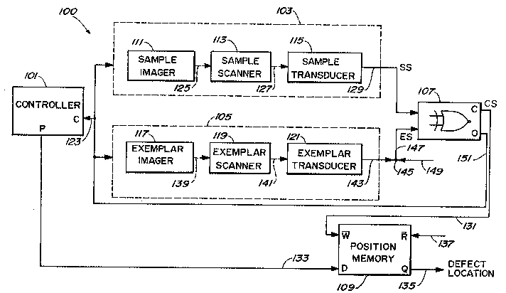
In accordance with the present invention, a quality inspection system 100
comprises a controller 101, a sample analyzer 103, an exemplar analyzer 105,
a comparator 107, and a position memory 109, as shown in FIG. 1. Sample
analyzer 103 includes a sample imager 111, a sample scanner 113, and a
15sample transdurer 115; likewise, exemplar analyzer 105 includes an exemplar
imager 117, an exemplar scanner 119, and an exemplar transducer 121.
The purpose of quality inspection system 100 is to provide for a rapid and
concise comparison of the three-dimensional forms of a sample 201 and an
exemplar 203, schematically shown in FIG. 2. Exemplar 203 is an exemplary
20 wafer at some stage of integrated circuit processing; sample 201 is a wafer at
the same stage of processing whose quality is to be determined. Potential
defects are indicated wherever sample 201 differs from exemplar 203.
Controller 101 is coupled to analyzers 103 and 105 via a control bus 123
for coordinating the actions of the analyzers' components, as shown in FIG. 1.
OPA*903 PATENT
2C~ i9
The individual lines of bus 123 are described below. Sample imager 111
provides an interferometric image which is transmitted via beam path 125 to
sample scanner 127, which scans the sample image to yield a sample scan in
the forrn of a time-varying intensity. The sample scan is transmitted via beam
S path 127 to sample transducer 115 which converts it to an electrical signal SSin which signal level corresponds to scan intensity. For signal SS, voltage
varies with time just as intensity varies with spatial position in the
interferometric image of sample 201. Signal SS is transmitted via line 129 to
comparator 107.
Comparator 107 compares sample signal SS with an exemplar signal ES,
in effect, providing an exclusive-nor (XNOR~ logical combination of the
signals. In other words, the comparison signal CS output from
comparator 107 is high when SS and ES are the same and low when they are
different. Comparison signal CS is transmitted via line 131 to the write
enable input of position memory 109. When activated by a logic low (when
SS is different than ES), position memory 109 stores position data received
at its data port via line 133 from the position data output P of controller 101.A host system can read the stored position data along line 135 from the
output of position memory 109 by enabling its read enable port via 137.
These operations are performed in conjunction with conventional addressing,
the ports and lines for which are irnplied in FIG. 1.
Exemplar signal ES can be generated concurrently with sample signal SS.
An exemplar image is transmitted from exemplar imager 117 via beam
path 139 to exemplar scanner 119. Exemplar scanner 119 transmits the
scanned exemplar image along beam path 141 to exemplar transducer 121.
Exemplar transducer 121 converts the resulting exemplar scan into exemplar
signal ES and transrnits this signal via line 143, node 145, and line 147 to
comparator 107.
ORA*903 PATENT
X(~3~59
11
Comparator 107 can also receive an exemplar signal along line 149 from
a host computer. In this case, exemplar signal ES does not result from
concurrent imaging and scanning of an exemplar along wi~h a sample. The
exemplar signal can result from a retrieval of a previously stored exemplar
5 signal, previously generated using interferometric imaging and scanning or it
can be a simulated exemplar signal generated from a computer model for the
design of the sample. Thus the present invention provides for flexibility in
selection of exemplar signal sources.
Since it can be impracticable to cover an entire wafer in a single scan,
- 10 quality inspection system 100 is designed to scan a sample region-by-region.
Controller 101 controls the X-axis and Y-axis movement of a translation
stage 205 via an X-drive 207 and a Y-drive 209 to select a region to be
analyzed. X-drive 207 is coupled to control bus 123 via a line 211 and is
mechanically coupled to stage 205 via a link 213; Y-drive 207 is coupled to
control bus via a line 215 and is mechanically coupled to stage 205 via a
link 217. Since sample 201 and exemplar 203 are both positioned on
stage 205, their initial alignment is maintained throughout the process of
locating defects.
The step-wise motion of stage 205 defines regions of sample 201,
20 including regions æ1, 227 and æs. The same motion also defines regions of
exemplar 203, including regions 231, 237 and 238. For example, sample
region 227 and exemplar region 237 are analyzed simultaneously. With
sample 201 and exemplar 203 properly aligned, exemplar region 237 includes
features which, in the absence of defects, should be duplicated in sample
25 region 227.
Quality inspection system 100 compares interferometric irnages rather
than pixel-based images. The appearances of sample 201 and exemplar 203
to their respective imagers 113 and 119 are indicated for sample regions 227
and æ8 and exemplar regions 237 and 238. For example, sample region 227
ORA~903 PATENT
2C~3~59
12
provides a generally rectangular curve corresponding to a peak 241 of a local
feature. Curves 242, 243 and 244 indicated successively lower contour lines
corresponding to the same feature. An essentially identical feature is located
in exemplar region 237, hence the correspondence of curves 251-254 with
lines 241-244.
Sample region 228 differs from corresponding exemplar region 238.
Specifically, sample region 228 does not include curves corresponding to
cunes 261-263 of exemplar region 238. These curves correspond to the
highest points on a local feature which also defines curves 264-267 in
exemplar region æ8. This type of discrepancy indicates that the top of the
corresponding feature on sample 201 either failed to form or was destroyed
so that sample region 228 only includes curves 274-277 corresponding to
curves 264-267 of exemplar region 238.
A major function of quality inspection system 100 is to signal the
difference between sample region 228 and exemplar region 238 while they are
being scanned so as to indicate the location of the difference and presumed
defect of sample 201. Since controller 101 determines the region being
scanned, the region of a detected difference is known a pnon. The position
within a region is determined by the scan position of sample scanner 113.
Sample scanner 113 effectively scans a transversely elongated slit
longitudinally across the region being scanned. The area viewed by the slit
at one instant during a scan is indicated schematically by rectangle 281 in
sample region 221, while the direction of scan is indicated by longitudinal
arrow 283. Rectangle 291 indicates the area scanned by exemplar
scanner 121 at the same instant, while arrow 293 indicates the direction of
scan for exemplar region 231. Controller 101 deterrnines the position of each
slit at each instant during a scan. When a difference is detected, the current
slit position is used to deterrnine a defect's longitudinal position within a
sample region.
ORA*903 PATENT
2~C~3~59
13
FIG. 3 depicts height versus longitudinal position profiles for
corresponding sample and exemplar regions, such as regions 228 and 238.
Profile 300 is a profile of an exemplar region, and profile 320 is a profile of
a corresponding sample region. Profile 320 is shown as a broken line where
it deviates from profile 300; elsewhere, the profiles are superimposed.
Profiles 300 and 320 are plotted over a range of heights (H1-H6) versus
longitudinal positions P1-P17. Each unit height represents the height
resolvable by the interferometric imager employed, e.g., sample imager 111
or exemplar imager 117, and is a function of the wavelength employed in
obtaining an interferometric image. Each unit of position corresponds to the
longitudinal extent at the region being scanned corresponding to the width of
the slit used in scanning. Height is not resolved along the length of a slit, soeach height is an integration over the transverse extent of a region. Of
course, at the cost of scanning speed, the slit can be made shorter. In the
limit imposed by diffraction, the "slit" can be one-half wavelength square, e.g.,
about 10 microns on a side.
Exemplar analyzer 105 yields a exemplar signal ES which appears ~s
signal 340 when profile 300 is scanned. Signal 340, which is idealized for
expository purposes, is high except when a canceIlation curve, such as
curve 265, is ~eing scanned, in which case, signal 340 goes low. A
cancellation curve occurs at positions in which a profile crosses a unit height
. . .
interval. For example, during T1, P1 is scanned and profile 300 remains
between H1 and H2 so no cancellation curve is encountered and signal 340
remains high. During T2, P2 is scanned and profile 300 crosses H2; a
cancellation curve is encountered and signal 340 goes low.
Sample analyzer 103 yields a sample signal SS which appears as signal 360
when profile 320 is scanned. Signal SS is generated in the same manner as
signal ES. Therefore, signals 340 and 360 are identical during tirnes
corresponding to positions over which profiles 300 and 320 are identical.
.
ORA~903 PATENT
2(~3~59
14
Profiles 300 and 320 are identical for positions P1-P6 and P14-P18;
consequently, signals 340 and 360 match for time intervals Tl-T6 and T14-
T18. Deviations betveen signals SS and ES indicate differences in the
profiles scanned; for example, profiles 300 and 320 are different over
5 positions P7-P13, and this difference is reflected in differences between
signals 340 and 360 during time intervals T7-T13.
Comparator 107 functions as an X-NOR gate, yielding a signal CS from
the combination of ES and SS. Accordingly, signal 380 is generated from
signals 340 and 360. Signal 380 is low during time intervals T7, T8, T11 and
10 T12, accordingly, positions P7, P8, P11 and P12, and the XY coordinates for
the region being scanned are transmitted. The position data generated fairly
characterizes the differences in between profiles 300 and 320, which extend
from P6-P13.
In general, sample signal SS is generally not synchronous with exemplar
15 signal ES so comparison signal can include pulses with fractional durations,
the fractions corresponding to phase differences between the sample and
exemplar interference patterns. This phase information can be used to allow
a measure of the degree of discrepancy between sample and exemplar.
Accordingly, a replica of CS can be inverted, integrated, digitized and fed
20 back to controller 101.
Digitized phase information is provided by comparator 107 at its ~ output
and transmitted to controller 101 via line 151 and bus 123. Controller 101
can then pass this phase information along with position information to
position memory 109. When a host computer accesses memory 109, it can
25 acquire the phase information relating to a defect as well as its position.
,
In the event that several nearby defect positions have similar associated
phases, this indicates a regional defect rather than a highly localized defect.
For example, in comparing interferometric sample and exemplar images, it
ORA*903 PATENT
2(~03159
- " 15
could be that the same fringe patterns are there, but one pattern is slightly
displaced with respect to the other. This could happen due to a misalignment
of part of an integrated circuit pattern or due to a difference in the
thicknesses of the region to which the defect position data relates. The phase
5 data can help distinguish such defects from strictly local defects and provide important guidance in improving the manufacturing process.
The method of the present invention is depicted in the flow chart of
FIG. 4. At step 401, an interferometric image of sample 201 is obtained,
yielding an interferometric image as shown with respect to region 228. At
step 402, this interferometric image is scanned by sample scanner 111.
Scanning effectively convelts position to time and the interferometric curves
to a time-va~ing intensity. At step 403, the time-varying intensity is
converted by sample transducer 117 to sample signal SS as represented by
signal 360. At step 404, signal SS is compared with exemplar signal ES, as
represented by signal 34Q yielding comparison signal CS, represented by
signal 380. At step 405, comparison signal CS is used to trigger the
generation of position data used to indicate the location of deviations in a
sample profile from an exemplary profile and thus indicate the location of
sample defects. Note that while the method is described as a series of steps,
the steps are sequential only on a quantum scale, i.e., as experienced by
photons and electrons. Operationally, all steps are executed concurrently.
Exemplar signal ES can be generated by analyzing an exemplar
synchronously with a sample. Thus, step 411 involves interferometric imaging
of exemplar 203 concurrently with step 401. Exemplar 203 is scanned in
step 412 synchronously with the scanning of sample 201 in step 402.
Exemplar signal ES is provided in step 413, just as sample signal SS is
provided in step 403.
Sample imager 111 is shown in greater detail in FIG. S; exemplar
imager 117 is essentially equivalent and so is not described separately.
ORA*903 PAll~l`JT
2~3159
16
Sample imager 111 comprises a variable intensity laser 501, a main beam-
splitting mirror 503, a reference plane 50S, a reference objective lens 507 and
a sample objective lens 509 arranged in a conventional interferometric
configuration. Additional components including a sample beam-splitting
mirror 511, a sample sensor 513, a reference beaIn-splitting mirror 515, a
reference sensor 517, a differential amplifier 519 and an attenuator 521 are
used to compensate for differences in reflectivity between sample regions.
The output of variable laser 501 traverses beam path 523 to main beam-
splitting mirror 503. The "sample" laser component reflected thereby is
transmitted along beam path 525 and most of it passes through sample bearn-
splitting mirror 511 to beam path 527. This sample laser component is
focused by sample objective lens 509 along beam path 529 onto sample 201.
Sample 201 reflects the incident beam, introducing phase distortions as a
function of the sample profile. The phase distorted beam is transmitted along
beam path 531, through objective lens 509 and along beam path 533 to
sample beam-splitting mirror 511. Most of the light reflected from
sample 201 is transmitted through sample beam-splitting mirror 511 and along
beam path 535. Half of the light along beam path 535 contributes to the
interference pattern output along beam path 125 to sample scanner 113, the
remaining half necessarily being diverted toward laser 501.
The "reference" laser component transmitted through main beam-splitting
mirror 503 is transmitted along beam path 537, mostly through attenuator 521,
along beam path 539, mostly through reference beam-splitting mirror 515,
along beam path 541, through reference objective lens 507, and along bearn
path 543 to reference plane 505. The incident light is reflected, ideally
without phase distortions, back along beam path 545, through reference
objective lens 507, along beam path 547, mostly through reference beam-
splittiIlg mirror 515, along beam path 549, mostly through attenuator 521 and
along bearn path 551 to main beam-splitting mirror 503. Half of this
reference beam is reflected by main beam-splitting mirror 503 and this half
ORA~903 PATENT
2(!~)3159
- 17
interferes with the sample component from beam path 535 to produce fringe
patterns along beam path 125, such as those shown superimposed on
regions 227 and æs in FIG~ 2.
A fraction of the light reflected by sample 201 and transrnitted along
beam path 533 is diverted by sample beam-splitting mirror 511 along beam
path 553 to sample sensor 513 to provide a measure of the overall reflectivity
of the sarnple region being scanned. Sample sensor 513 thus provides a
control signal, along line 557 and branch 559, through a summing
amplifier 563, and along line 561 to variable laser 501. This control signal is
used to control the intensity of the output of variable laser 501 to compensate
for differences in reflectivity across sample regions.
Without additional compensation, the contribution of the reference beam
along beam path 551 to the interferometric image along beam path 125
changes with the output intensity of variable laser 501. Since laser output
intensity is varied to provide for a relatively constant intensity for the sample
component of the interferometric image it is desirable to maintain a
substantially constant intensity for the reference component as well. To
maintain a reference beam of substantially constant intensity the reference
beam must be variably attenuated to compensate varying laser output.
Branch 567 from line 557 carries the sample sensor output to the "+" input
of differential arnplifier 519. In addition, reference beam-splitting mirror 515diverts a fraction of the reference beam along beam path 547 to reference
sensor 517 via beam path 569. The output of reference sensor 517 is directed
along line 571 to the "-" input of differential amplifier 519. The output of
differential amplifier 519 is directed along line 573 to attenuator 521 which
is regulated to compensate for changes in laser intensity. More speclfically,
the arrangement including differential amplifier 519 forces the overall
intensity of the reference beam along beam path 551 to traclc the overall
intensity of the sample beam along beam path 535. In this way, the intensities
of the components of the interference are balanced within an optimal
-
ORA~903 PATENT
.:
2(~C)31~9
18
intensity range, which condition provides the most distinct interference patternto sample scanner 113~
Variable intensity lasers are typically configured with a pair of polarizers
which can be rotated relative to each other to attenuate laser output. Instead,
S variable laser 501 uses an occluding pinhole, as described with reference to
FIG. 6. Variable laser 501 comprises conventional components including a
laser 601, a converging lens 603, a pin-hole spatial ~Iter 605, and a
collimating lens 607. A pin-hole occluder 609 is mounted on a base 611
which can be moved between converging lens 603 and spatial filter 605 when
an occluder drive 613 is actuated. In addition, laser 501 employs a system
beam-splitting mirror 615 so that it can be used by exemplar imager 117 as
well as sample imager 111~
The output of laser 601 is transmitted along beam path 617. The
component of the laser output transmitted through system beam-splitting
mirror 615 is transmitted along beam path 619 to converging lens 603. The
laser beam along beam path 621 converges toward the pin-hole of spatial
filter 605. However, to an extent depending on its longitudinal position,
occluder 609 blocks a portion of the light along beam path 621 and transmits
the remairling portion along beam path 623 to spatial filter 605. The light
diverges along beam path 625 and is collimated by collimating lens 607 to
provide the output of variable laser 501 along beam path 523.
The longitudinal position of occluder 609 between converging lens 603
and spatial filter 605 is controlled by the output of sample sensor 513 along
branch 563, which actuates occluder drive 613. Occluder drive 613 is
mechanically linked to occluder base 611 via link 629. Arrows 631 indicate
the directions of motion available to occluder 609. Movement toward
converging lens 603 decreases laser output intensity while movement toward
spatial filter 605 increases laser output intensity~ The component of the
output of laser 601 reflected along beam path 627 by system beam-splitting
ORA~903 PATENT
2C~3159
19
mirror 615 is used for exemplar imager 117 in the same manner as the
component transmitted therethrough is used for sample imager 111.
Sample scanner 113 comprises a scanning prism 701 and a frame 703 for
a slit 705, as shown in FIG. 7. Controller 101 controls the motion of scanning
S prism 701 using a scan drive 707. The scan position of scanning prism 701 is
monitored using an optical encoder 709. Scanning prism 701, scan drive 707
and optical encoder 709 are shared by exemplar scanner 119. In addition,
exemplar scanner 119 includes a frame 711 for a slit 713. Since sample
scanner 113 and exemplar scanner 119 share scanning prism 701,
synchronization of the sample and exemplar scans and thus of sample signal
SS and exemplar signal ES is straightforward.
An image, such as that represented in sample region 228 of FIG. 2, is
transmitted from sample imager 111 along beam path 125 to scanning
prism 701. Scanning prism 701 refracts incident light at an angle dependent
on its instantaneous orientation, which is continually changing due to the
action of scan drive 707, which is basically a DC motor. Thus, the portion of
the beam transmitted along beam path 715 and incident slit 705 changes as
- scanning prism 701 rotates. As a result, the portion of the image transmitted
along beam path 127 to sample transducer 115 is continually changing.
The portion of the sample image passed by slit 705 is represented in
FIG. 2 by rectangle 281, which is the reverse projection of slit 705 onto
sample region Z1. Arrow 283 corresponds to the rotational direction of
scanning prism 701. As a result of the scanning, the portion of the sample
image transmitted along beam path 127 to sample transducer 115 sometimes
includes a dark interference band and sometimes does not. When it does,
sample signal ES is low, otherwise it is high. The transitions can be made
shalp using a threshold device as explained below with reference to FIG. 8.
As discussed above, the output of sample transducer 115 is directed along
line 129 to comparator 107.
ORA~903 PATENT
2(~ ';9
The exemplar image, which is represented by curves 261 267 for exemplar
region 238 in FIG. 2, is processed concurrently and in a similar marmer. The
exemplar image is received from exemplar imager 117 along beam path 139
and variably refracted by scanning prism 701. The variably re~acted image
is transmitted along beam path 717 to slit 713. The reverse projection of
slit 713 onto exemplar region 231 is shown by recta~e 291 in FIG. 2, while
the rotational direction of scanning prism is represented by arrow 293. The
scanned portion of the exemplar image is transmitted along beam path 141
to exemplar transducer 121. The output of exemplar transducer 121, which
corresponds to exemplar signal 340 in FIG. 3, is transmitted along line 143
toward comparator 107.
Scan drive 707 and optical encoder 709 are controlled by controller 101
via control bus 123. Scan drive receives control signals, e.g., on and off, fromcontrol bus 123 via line 719 and mechanically executes the embodied
commands via link 721. Optical encoder 709 detects the passage of strobe
marks on a shaft of scanning prism 701 via beam path 723 to monitor its
rotational position. The results are transmitted along line 725 and control
bus 123 to controller 101 for use by position memory 109.
Sample transducer 115 comprises a photo-multiplier 801, a threshold
device 803, a sample-and-hold circuit 805, a differential circuit 807, and a one-
shot 809, as shown in ~IG. 8. The sample scan is received along beam
path 127 by photo-multiplier 801. The sensitivity available in photo-
multiplier's is typically around 10,000 times that available from CCDs; this is
a reason for the superior performance of quality inspection system 100
relative to those based on CCD imaging. The signal output along line 811
varies in proportion to the intensity of the scanned input to photo-
multiplier 801. Threshold device 803 is used to obtain a binary output such
as those shown by sample signal 360 in FIG. 3. l'his binary output serves, via
line 129, as the input enable to position memory 109.
ORA*903 PATENT
2(~3159
21
The interferometric sample image is a superposition of an interferometric
pattern on a reflectivity distribution corresponding to the region of the samplebeing scanned. When sample slit 705 is not viewing an interference fringe,
the photo-multiplier output basically represents the reflectivity pattern.
5 Accordingly, variable laser 601 can be adjusted to compensate for reflectivityat a spatial frequency corresponding to a couple of slit widths using feedback
based on the photo-multiplier output.
To this end, sample-and-hold circuit 805 is arranged to sample the photo-
multiplier output during scan times when no fringe is being viewed by sample
10 slit 705 and to hold sampled values during scan times when a fringe is viewedby slit 705. Differential circuit 807 and one-shot 809 provide the timing for
the sample-and-hold operation. The photo-multiplier output can be roughly
characterized as a constant signal with downwardly pointing trapezoidal pulses
corresponding to the appearance of fringes in the slits field of view.
15 Differential circuit 807 converts this waveform to a ground level signal
followed by a narrow downward spike followed by another ground level signal,
and then an upward spike. The upward spike is followed by another ground
level signal corresponding to the next "inter-fringe" portion of the scan cycle.
The spike pattern is transmitted to one-shot 809 via line 813. One
20 shot 809 responds only to upward spikes to which it responds with a clean
pulse of a fixed duration about one half the minimum expected fnnge
separation in an interferometric image. The one-shot output is transmitted
along line 815 to a clock input of sample-and-hold circuit 805. Sample-and-
hold circuit 805 samples while the one-shot output is high and holds while it
25 is low. This has the desired result of sampling when no fringes are being
viewed and holding while fringes are being viewed.
The sample-and-hold output is transmitted along line 565 which is an
input to summing amplifier 563 which controls variable laser 501. In effect,
. .
ORA~903 PATENT
,~ ' ~ ' .
Z(~3~59
Z
the described feedback from sample transducer llS provides high spatial
frequency reflectivity filtering in addition to the low spatial frequency
reflectivity filtering provided by the feedback from sample sensor 513. The
two levels of reflectivity filtering maintain an optimal signal-to-noise ratio
5 throughout quality inspection system 10Q.
Quality inspection system 100 is designed so that regions can be scanned
in rapid succession. For this to happen, it is necessary that stage 205 be
positioned with great precision, e.g., to within 1 ~m, and with great speed. In
other systems, precise positioning implies signifisant mechanical isolation from10 ambient shocks and vibrations. To the contrary, quality inspection system 100uses ultrahigh speed, closed loop positioning to offset vibrations so that
elaborate mechanical isolation devices need not be employed.
High speed positioning is provided in part by asynchronous operation of
X-drive 207 and Y-drive 209. Movement in each axis, e.g., X and Y, is
15 directed independently of movement in the other. Thus, movem~nt along
each is optimized without concern for the speciSc path taken to reach a
desired endpoint. Movement of stage 205 along each axis is monitored by a
respective laser interferometer. Position feedback from each interferometer
is compared with a programmed destination to set optimal speed during stage
20 travel. For example, when feedback indicates that the stage is within a
predetermined range of the destination for the respective axis, the speed
decays to provide a smooth stop at the desired point. Comparison of
monitored position with destination is performed in real-time by dedicated
circuitry so there is no need to wait for microprocessor intervention.
Actual positioning is provided using enhanced precision stepper motors.
X-drive 207 and Y-drive 209 use identical stepper motors, so only the motor
for X-drive 207 is described in detail. This stepper motor is conventional
except as to the signal used for driving it. The stepper motor includes a
threaded shaft which is rotated by a changing magnetic Seld. The precision
ORA~903 PATENT
'''''' ~
2C~3~.59
: 23
of the stepper motor is determined in part by the pitch of the thread: a finer
pitch permits more precise positioning. However, there are
material/mechanical limits to how fine a pitch can be used. X-drive 207 uses
a uniquely driven stepper motor to provide greater positioning precision for
5 any given pitch of the shaft threads.
The stepper motor includes multiple coils, each dedicated to driving a
respective "phase" of the motor. Typically, the coils are driven in alternation
by binary signals. The binary signals are out-of-phase with respect to each
other so that the coils activate magnetic fields in turn, urging a rotor and the10 attached shaft to turn.
The stepper motor used in X-drive 207 is not driven by bi-level signals,
but rather by multi-level signals. The multi-level signals are generated by
repeated sampling and holding of a rectified cosine wave. The result is a
step-wise approximation of a rectified cosine wave. The drive signals are
15 staggered with respect to each other. Since the present stepper motor uses
two coils, the drive signals are generated out-of-phase so that one reaches its
maximum while the other is at its minimum. The corresponding coils are
arranged orthogonal to each other, as in a convention stepper motor. The
effect of the stepped cosine signals is that, instead of acting in alternation,
20 they add vectorially, tracing a circle over time. While a conventional stepper
motor might have four discrete rotational positions per revolution, the present
stepper motor has as many as there are sample-and-hold steps over half a
cosine cycle. Thus, the precision of a conventional stepper motor is
significantly enhanced.
The present invention provides for modifications, variations and
extensions to quality inspection system 100 as described above. Provisions are
made for alignment of fringes, variations on scanning, reflectivity filtering, and
signal processing. Furthermore, provisions are made for taldng metrologies
about locations identified for possible defects.
ORA*903 PATENT
2(~03159
24
The signal-to-noise ratio for sample signal SS is greatest when fringes are
aligned with slit 705. When fringes are not aligned with the slit, the slit views
several fringes and intermediate spaces at once, rather than in sequence. The
bright spaces and dark fringes are integrated over the slit, yielding an
intermediate signal which is difficult to interpret.
In a typical integrated circuit, most of the features extend along either
one of two orthogonal axes. Therefore, it is usually feasible to align a sample
integrated circuit so that roughly half of the interference fringes are aligned
with slit 705. A lesser percentage is attainable for samples with irregular
features.
Discrepancies in fringes not aligned with slit 705 are difficult to detect.
This raises the questions as to whether defects are being missed by the
scanning method describe above. The answer, for the most part, is no.
Generally, a defect causes discrepancies in fringes extending in several
different directions. While discrepancies in fringes not aligned with a slit maynot be detected, the defects causing those discrepancies can be detected by
discrepancies in other fringes that are aligned with a slit. Thus, while some
of the data reflected in a defect is rnissed, the defect itself is located.
Nonetheless, the chances of detecting defects can be enhanced by
adjusting the alignment of fringes with a slit by rotating the incorporating
interferometric image relative to the slit. The information used for alignment
can be encoded with position data to characterize the local slope of the
fringes. This relative rotation can be provided by rotating sample frame 703
- and thus slit 705 relative to a stationary sample image. Similarly, exemplar
slit 713 can be rotated relative to the exemplar image. Frarne 703 can be
marked so that its rotational position can be monitored by an optical encoder.
When sample slit 705 and exemplar slit 713 are aligned differently, the
difference can be calculated and stored as defect data.
ORA~903 PATENT
.'
2~03159
It is also possible to move the image relative to a stationary slit, for
example using a dove prism. A dove prism is an optical device which, when
rotated through an angle, can rotate an image through twice that angle. Thus,
alignment can be effected by rotating a dove prism configured along the
5 image path.
The effect of the dove prism depends on its position along the beam path
relative to scanning prism 701. A dove prism between scanning prism 701
and slit 703 rotates the sample image after it is swept; the scan direction
(arrow 283) relative to the region being scanned is unchanged, but the angle
10 of the back-projection (rectangle 281) of the slit onto the region is changed.
If scanning prism 701 is between the dove prism and slit 705, then the
image is rotated before it is swept; this changes the direction of the scan
relative to the sample. In other words, arrow 283 in sample region 221
becomes tilted relative to its position as shown in FIG. 2. In effect, back-
projection rectangle 281 is rotated with scan direction arrow 283 so that
slit 705 extends orthogonal to the scan direction. Therefore, the region
scanned is orientated obliquely relative to sample regions æ1, 217 and 218
of FIG. 2.
To achieve the desired alignment, whether by rotating a slit or a dove
20 prism, actual alignment must be detected. This can be done using a quad
detector, which is a device with four photo-electric quadrants, which can be
labeled A, B, C and D going clockwise about the center of the device. The
quad detector can be aligned so that the boundary between quadrants B and
C and between quadrants D and A is aligned with slit 705. (More specifically,
25 a fringe aligned with this boundary is also aligned with slit 705.) The outputs
of the quadrants can be coupled to differential amplifiers to provide an output
E = (A-D) - (B-C). This output E is zero when the fringe or fringes
incident to the quad detector are properly aligned. Othelwise, output E is not
ORA~9Q3 PATENT
2(~ 159
- 26
zero and can be used as a control signal to effect a relative rotation until thedesired alignment is achieved. A corresponding configuration can be used for
exemplar slit 713.
The quad detector can be selected to correspond to the area viewed by
slit 705 or to correspond to a larger area, such as region 221. The advantage
of a larger area is that the scan direction and slit alignment can be optimized
for a given region and then maintained during the scan. However, more
precise alignment on a fringe-by-fringe basis requires that the quad detector
area correspond to the slit area. In this case, the quad detector should be
arranged to receive a portion of the interferometric image after it is swept by
scanning prism 701. The quad detector can be mounted on frame 703, which
has the advantage that it rotates with slit 705. Otherwise, the quad detector
can be mounted in some other rigid relation relative to slit 705.
The quad detector can intercept the same sweep received by the slit. For
example, the quad detector can be placed to anticipate the slit's view.
Alternatively, a beam-splitting mirror can be used to generate a parallel
image, which is also swept by scanning prism 701 so that the quad detector
and slit 705 view the same portions of the interferometric image at the same
time.
If the quad detector is selected to view the entire region being scanned,
a beam-splitting mirror can be used to divert a portion of the image beam
along beam path 125 before it is swept. This diverted portion is directed to
the quad detector. This approach is useful for detecting defects in which an
entire region of an integrated circuit may be misaligned relative to the rest
of the integrated circuit. In this event, the sample image will be aligned
differently than the exemplar image. The difference in the sample and
comparison alignment signals can then be used as an alternate enable signal
for the position memory.
ORA*903 PATENT
13159
27
Feedback from the quad detector, or other orientation sensor, can be
used in several ways. It can be used to rotate: a slit; a dove prism placed
before or after the scanning prism, or stage 2~5 to a desired orientation. It
can be used to select among several slits at different fixed orientations as the5 source for the scan. In this case, each slit can have its own photo-multiplier.
In addition7 the multiple slit approach can employ means for comparing the
outputs of several slits at once and selecting the slit output with the strongest
fringe definition. Slit selection can be monitored to provide orientation
information on the fringes. Another approach to handling fringes at different
10 angles is to perform multiple scans.
In the illustrated embodiments, reflectivity filtering is performed using
light reflected from a sample region and also using the sample signal level to
regulate laser output. The light reflected from the sample re~.on provides
reflectivity filtering on a region-by-region basis. By using a CCD sensor as
15 sample sensor 513, one can obtain the information required for pixel-by-pixel reflectivity ~lltering prior to scanning. The CCD can be "read-out"
synchronously with the scan process to provide the desired filtering.
Instead of attenuating the overall laser output7 one can use a pixel-based
attenuator, i.e., one in which the sp~tial distribution of attenuation can be
20 controlled. The output of the CCD sensor can be used to control the spatial
distribution of attenuation to complement the spatial distribution of
reflectivity of the sample.
An attenuator can be placed in the sample arm of the interferometer,
e.g., in beam paths 525 and 535. In this case7 only a single attenuator is
25 required, obviating the need for attenuator 521 to compensate intensity
variations in laser 501 (which would be held at constant intensity). The
attenuator in the sample arm could be uniform or pixel-by-pixeL These
approaches to separating form from reflectivity can be replaced or
complemented by mathematical deconvolution of the interferometric image.
ORA~903 PATENT
2~03159
28
In sample analyzer 103, an interferometric image is created and then
scanned. Alternatively, the laser itself can be scanned over a sample region,
much as a laser in a laser printer is scanned over the drum. In this case,
there is never a complete interferometric image of a sample region. The scan
5 is produced directly from the sample so it is not necessary that irnaging and
scanning be performed by separate components.
The scan converts the spatial distribution of intensity of the
interferometric sample image to a temporal distribution of intensity. In other
words, the scan is an optical signal which characterizes the interferometric
10 sample image. Current technology favors processing electrical signals, so
transducer 115 is provided to convert the optical signal to an electrical signal.
However, the present invention provides for direct optical comparison of
sample and exemplar scans to generate an optical comparison signal. In this
case, the optical comparison signal can be further optically processed or
15 converted to electrical form for electrical signal processing.
An alternative method of producing a comparison signal CS is to arrange
sample 201 and exemplar 203 in a single interferometer arrangement. In
other words, exemplar 203 can be positioned in place of reference plane 505
in sample imager 111. The resulting interference pattern shows the
20 differences between the sample and the exemplar. This interference pattern
can be scanned and converted to an electrical signal to provide the
comparison signal. This has the advantage of requiring only one
interferometer. The disadvantage is that it does not permit recorded and
simulated exemplar signals to be compared with the sample signal.
Sample transducer 115 includes a threshold device 803 so that it provides
a binary sample signal SS at its output 129. Alternatively, this device can be
omitted in the transducer so that SS and correspondingly exeTnplar signal ES
are analog. The advantage of this approach is that SS, ES and an resulting
ORA*9()3 PATENT
2(~ 59
29
unthresholded CS can more sensitively reflect their referents. The amplitude
of differences and the tirning of transitions can both be used to indicate the
nature of detected discrepancies. A threshold device can be applied to a
replica of the comparison signal CS to provide binary control for position
5 memory 109.
The method of the present invention, as described above with reference
to FIG. 4, yields a list of positions of potential defects. This list can be used
to guide further analysis of sample 201. Specifically, one might vish to
characterize precisely the form of an area about a defect location, i.e., obtain10 a metrology of the defect location. Such a metrology can be used using
quality inspection 100 or a modification thereo The basic idea is to use an
interferometric image of a sample rather than a normal sample image, since
the former provides form data in a purer form.
The main advantages of the interferometric images are that they
15 represent three-dimensional form and that they represent it simply. The
relative simplicity of an interferometric image compared to a normal image
allows it to be described in a very compact format, which, in turn, saves
storage space, comrnunications bandwidth and processing time. For the
purposes of a metrology, the information of interest is the two-dimensional
20 shape of each fringe, its size, its location (relative to neighboring fringes), and
its orientation (relative to neighboring fringes). Preferably, this is
supplemented by relative height data.
The relative heights represented by the respective fringes in the
interferometric sample image can be distinguished by comparing it to a
25 second interferometric sample image taken under a slightly different angle ofillumination The information provided by the second interferometric sample
irnage can be encoded concisely into a representation or description of the
first interferometric sample image. For example, each fringe in the first
irnage can be assigned a height in half-wavelengths relative to an arbitrarily
ORA*903 PATENT
selected fringe or to a fringe whose absolute height is known a priori.
Alternatively, both interferometric sample images can be maintained for later
reconstruction or analysis. Another approach to resolving height sign
ambiguity is to supplement interferometric analysis with a cruder analysis of
5 a height profile. For example, one can use an objective lens with a shallow
depth of field and move it relative to the sample and determine what parts
move into focus and which move out of focus.
Even the crudest encoding of an interferometric image for a metrology
can be a bit map, with one bit per pixel. No grey-scale irlformation is
10 required as would normally be used with a standard image. Since grey-scale
is not required, there are several compacting algorithms that could effectively
compress the bit map. Furtherrnore, the width of a fringe is not required.
Therefore each fringe can be assigned, for example, a width of one pixel. A
raster representation could be a series of numbers representing the number
15 of pixels between interference fringes on each raster line of the
interferometric image. Even more efficient compacting can be achieved by
analyzing an interferometric into graphics primitives and coding the
interferometric image accordingly as a computer-aided design data file, e.g.,
an Autocad file, a forrnat defined by Autodesk, Inc., or a page description file,
20 e.g., a Postscript file, a format defined by Adobe Systems, Inc. Such encoding
is not only compact, but also flexible. They make it easy to compare images
that are scaled, rotated or inverted relative to each other.
The encoding of an interferometric image can be performed using a
stored complete image or can be based on a scan of an interferometric image.
25 While using an image stored, for example, by a CCD, can introduced delays
in obtaining a metrology, these delays are more acceptable than delays caused
by image storage during initial inspection. This is because the initial
inspection permit metrologies to be limited to relatively few and relatively
small areas. The advantage of assembling a complete image is that there is
ORA~903 PATENT
2~)3~S9
31
more flexibility available to an encoding process in determining the most
compact and useful description of an interferometric image.
Nonetheless, assembling a metrology "on-the-fly" from a scan of an
interferometric image provides the best opportunity for real-time analysis of
5 a sample. A real-time metrology can be obtained using a slit wheel 910 in
conjunction with slit 705 as shown in FIG. 9. Slit wheel 910 includes eight
circumferential and evenly distributed radial slits 911-918. Scan drive 707
drives slit wheel 910 via mechanical link 921 in a counterclockwise direction
as indicated by arrow 923.
Radial slits 911-918 are circumferentially spaced so that exactly one radial
slit overlaps slit 705 at any one time. With slit wheel 910 oriented as shown
in FIG. 9, slit 912 overlaps slit 705. The area of overlap defines a pixel
window 931 which moves along slit 705 in the direction indicated by
arrow 933. As slit 912 moves past slit 705, slit 913 moves in a position to
overlap slit 705.
Slit wheel 910 should rotate fast enough for the entire interferometric
sample image to be scanned. The continuous spinning of scanning prism 701
causes the interferometric sample image to move transversely of slit 705 while
one of the radial slits, e.g., slit 912, moves longitudinally relative to slit 705.
If, during the time it takes slit 912 to pass slit 705, the image is moved more
than the width of slit 705, then there will be portions of the image that are
never viewed by pixel window 931. Thus, slit wheel 910 should rotate so that
at least one radial slit passes slit 705 for each slit-width of movement of the
image relative to slit 705.
Each slit 911-918 is long enough to overlap completely the width of
slit 705 anywhere along its length. Each slit 911-918 has the sarne width as
slit 705. Thus, pixel window 931 is a diffraction-limited square. The
interferometric sample irnage, as scanned by pixel window 931, is the input
ORA*903 PATEI`JT
ZC03159
32
to sample transducer 115. The output of sample transducer 115, i.e., sample
signal SS, represents the interferometric sample image on a pixel-by-pixel
basis. Accordingly, when slit wheel 910 is used, sample signal SS permits the
interferometric sample image to be reconstructed. The reconstructed
S interferometric sample image can be used to characterize the form of the
location of interest.
Sample signal SS is a serial representation of the interferometric sample
image corresponding to a selected location. Formatting sample signal SS into
blocks, with each block corresponding to one sweep of slit 705 by one of the
radial slits 911-918 provides a raster representation of the interferometric
sample image at the location of interest. Sample signal SS can be processed
in a variety of ways so that the metrology data it represents are presented in
a concise and useful format. For example, each block of formatted signal SS
can be recorded to represent the changes relative to the previous block in
15 fringe locations rather than absolute fringe locations. The resulting signal
represents the metrology of the location of interest independent of its
absolute position on sample 201. This form of the data can be most useful
when comparing metrologies for different locations or between metrologies
for a sarnple location and a corresponding location on exemplar 203.
When data is encoded in the form of changes between blocks, the
changes represent local slopes of fringes. Each fringe represented in a block
can be expressed by a linear approximation y = kx + c, where k is the slope
and c is a displacement along the y direction. Successive fringes can be
distinguished by the value of c This suggests that signal SS can be converted
to a string of data in the forms of slope values and displacement values, with
the slopes representing local tangents to fringes and the displacement values
representing spacing between fringes. Finally, the slope and displacement
data can be replaced by changes in slope and changes in displacement from
block to block. Such a representation would characterize the form of a
location independent of its orientation and absolute position for comparison
ORA*903 PATENT
. .
2(!03~59
33
with other locations which might include similar defects or features at
different orientations. Absolute position and absolute orientation can be
reconstructed as desired from the start position of the scan.
Another way to obtain a metrology, not using slit wheel 91Q is to use a
S quad detector or other means to maintain alignment of fringes and slit 705while monitoring the alignment to provide slope data for the fringes. The
relative motion of slit and image required for mutual alignment can involve
rotating frame 703, and thus slit 705, or rotating the image, for example using
a dove prism. Frame 703 or the dove prism can be optically encoded to
provide a reading of alignment position, which corresponds to slope data.
The quad detector would have an area on the order of that of slit 705 and be
arranged to receive the same portion of the image viewed by slit 705. The
output of the quad detector would be non-zero whenever a fringe is not
`- aligned with slit 705 and the non-zero would be used to drive the alignment
means until alignment is achieved. This approach yields a series of fringe
detections along with slope data for each fringe detected. This information
can also provide linear approximations of the form y = kx + c for the fringes.
Thus, permitting compact data storage and efficient reconstruction of
interferometric image of interest.
Another alternative is to trace ~inges while monitoring the tracing
procedure. A quad detector can be used to track the alignment of a fringe
with slit 705 and force the desired alignment to be maintained. Alternatively,
changes in the output of sample signal SS when slit wheel 910 is used can be
used to turn a dove prism to reorient the interferometric sample image with
slit 705. Instead of a single slit, multiple slits could be used. For example,
three pixel windows can be used. A center pixel window is used to trace a
fringe. Two outer pixel windows provide correction signals when either views
the fringe. This arrangement is analogous to that used in three-beam laser
piclc-up systems for compact discs. An output signal reflecting changes in
ORA~903 PATENT
2C~)31S9
34
alignment indicates form independent of absolute orientation and absolute
position. This facilitates comparison with other features and defects.
In another embodiment, a CCD imager is used to store an interferometric
sample image. The stored image is then vectorized into a compact data
S forrnat for transmission, storage and reconstructions. Since the defect location
process greatly limits the area of the wafer that must be analyzed, it can be
cost effective to use more time-intensive CCD imaging for the metrology.
Taking a CCD image of the interferometric image instead of the sample
directly emphasizes form over reflectivity. Use of the reflectivity filtering
10 techniques described above further enhances the fringes. The fringes can
then be characterized by their size, shape, orientations, and inter-fringe
spacing and gradient sign. The data format can be a series of commands
required for a plotter or other device to reconstruct the fringes. Intermediate
intensities and fringe thicknesses can be ignored in characterizing the sample.
15 Thus, the interferometric imaging approach eliminates irrelevant and
distraction information for the purposes of creating a metrology.
The foregoing procedures are alternative methods of encoding an
interferometric image. However, it is not generally apparent whether a fringe
represents a higher or lower level than a neighboring fringe. To resolve this
20 ambiguity, a second interferometric image can be used. This second image
can be obtained subsequently using a single beam imaging system by tilting
the sample. Alternatively, an imaging system can employ two beams at
slightly different angles relative to the sample. The differences between the
interferometric images can be made small so that there is no arnbiguity of
25 correspondence between the fringes of one image and the other. Pairs of
interference fringes move closer together when the gradient that they
represent corresponds to the direction of tilt and move farther apart when the
gradient is opposed to the tilt. This gradient information can be encoded
along with the form data for the fringes. For example, a data format might
`30 include slope data indicating the local tangent of a fringe, spacing data
~RA~903 PAlENT
31S9
indicating spacing relative to a neighboring fringe, and gradient direction
data indicating the gradient direction from the neighboring fringe to the
subject fringe.
Where the two interferometric images used to deduce height data are
S generated by two laser beams with different angles of incidence at the sample,
the interferometric irnages can be examined sequentially. This can be done
simply by scanning one interferometric image and then the other. However,
it is preferable to analyze the two images concurrently to permit real-time
metrologies. To this end, the two beams can have different frequencies or the
same frequency but different polarization. The imager output can be split
into two branches. One branch can be filtered to obtain one interferometric
image and the other branch can be filtered to yield the other interferometric
image.
The interferometric image of the first branch can be directed along beam
path 125 to scanning prism 701 (see FIG. 7) and the interferometric image
of the second branch can be directed along beam path 139, using
appropriately arranged mirrors. In this configuration, the outputs of sample
transducer 115 and exemplar transducer 121 represent the two interferometric
images of the sample.
Each transducer output is in the form of a pulse train. The variable of
interest is the duration between pairs of successive pulses. For example,
where the duration between one pair of successive pulses in the exemplar
transducer output is greater than the duration between a corresponding pair
of pulses in the sample transducer output, this can indicate that the fringe
corresponding to the latter pulse (in both pulse trains) represents a greater
height than the earlier pulse. This relationship could be reversed, but it is the
same for all pairs of pulses for a given configuration.
ORA*so3 PATENT
2~031S9
- 36
The duration information can be converted to amplitude information by
using the first pulse to trigger the charging of a capacitor and the second
pulse to stop the charging of the capacitor, as in a sample-and-hold
arrangement. This conversion is performed on the outputs of both
transducers 115 and 121. The resulting signals are then compared, e.g., using
a differential amplifier. The instantaneous sign of the differential amplifier
output then provides the height data to be correlated with the fringe data.
In all these metrology approaches, the distinctiveness of fringes can be
enhanced using reflectivity filtering. Low spatial frequency reflectivity filtering
can be performed on a region-by-region basis and high spatial frequency
filtering can be performed using feedbaclc from sample transducer 115.
As is apparent from the foregoing, the present invention provides an
enhanced quality inspection system, as well as options for modification,
variation and extension. In particular, a metrology extension is delineated
above. These and other modifications and variations are provided for by the
present invention, the scope of which is limited only by the following claims.
What Is Claimed Is:
ORA*903 PATENT