Note: Descriptions are shown in the official language in which they were submitted.
20032~;~
1 --
Docket No. 239-382
PRINTED CIRCUIT THERMOCOUPLE ARRANGEMENTS FOR PERSONNEL
TRAINING AND EQUIPMENT EVALUATION PURPOSES, AND METHODS
FOR MAKING AND USING SAME
Backaround of the Invention
The present invention relates to thermocouples
which are used in conjunction with printed circuit
boards for training personnel in soldering/desoldering
of leads of circuit components to the printed circuit
boards, as well as for conducting a quantitati~e
analysis of the performance of repair, rework, and
production equipment used for soldering/desoldering,
cleaning, preheating, and spot-welding of components
mounted to printed circuit boards. In particular, the
invention relates to the formation of thermocouples for
such purposes by standard printed circuit board
construction techniques, as opposed to standard
thermocouple construction techniques, as well as the
manner in which they can be made and used to emulate a
wide variety of circuit board types, layouts and
assembly configurations.
In commonly owned U.S. Patent No. 4,224,744,
circuitry for teaching soldering and a practice circuit
board for use therewith are disclosed, wherein a
training board having a plurality of terminals thereon
and wherein a plurality of temperature sensing devices
associated with the respective terminals are provided
at each terminal where the soldering of a joint is
attempted to monitor the performance of a trainee or
other person whose repair skills are being evaluated.
One form of temperature sensing means that is disclosed
is the provision of thermocouples at each of a
2003Z02
-- 2
plurality of through holes formed in a printed circuit
board. These thermocouples are comprised of a flrst
conductor, such as electroless copper, that is plated
through the holes so as to form pads or lands at each
of opposite sides of the printed circuit board, and a
metal foil or wire made of iron or constantan or some
other dissimilar conductor metal from that of the
plated through hole that is attached to one of the pads
or lands of the plated through conductor, whereby a
thermocouple junction is formed. For formation of
these thermocouple junctions, the use of electrical
arc, flame heating, soldering, swagging, welding,
brazing, beading, or butt-welding techniques are
disclosed. Furthermore, while this patent indicates
that its disclosure is also applicable to desoldering,
welding, etc., as well as to circuit connections other
than those on a single or double-sided printed circuit
board, such as multilayer boards, ceramic printed
circuits, etc., and various terminations such as plated
through holes, unsupported holes, funnelets,
eyelets, standoffs, etc., no structures, techniques or
applications are disclosed which are either directed to
the emulation of a wide assortment of circuit board
layouts, types and assembly configurations which vary
by component type, substrate material, thermal
characteristics and other factors, or to the
application thereof to the development, evaluation,
monitoring and adjustment of "thermally affecting"
production, rework or repair processes and equipment
used therefor, i.e., for soldering/desoldering,
preheating, spot-welding, etc.
Commonly owned U.S. Patent No. 4,224,744 also
discloses in detail the various factors which impact
upon ~he ability to perform high quality rework and
repair operations upon electronic assemblies, and this
~description is hereby incorporated by reference for the
2003202
sake of brevity. These factors include not only the
human factor, for which training to obtain the
requisite skills and experience to enable the operator
to observe the work and react appropriately in the
manipulation of the soldering iron or other rework and
repair device is the best insurance, but also includes
other factors which are not operator dependent, such as
the characteristics of the rework and repair device,
e.g., a soldering iron for which its idle tip
temperature, recovery rate, etc., and characteristics
of the component and printed cirouit board, such as
temperature, thermal conductivity, specific heat, etc.
AS a result, for proper training and evaluation of
personnel, it is desirable to be able to simulate as
realistically as possible a wide range of circumstances
an operator is likely to encounter. Also, even with
the best of training, the potential exists for
overheating the work, as a result of excessive dwell
times or temperatures, so as to cause printed circuit
board damage in the form of lifted pads, damage to
plated through holes, or, in extreme cases, damage to
the fiberglass laminate, etc., as a result of equipment
related factors. Thus, it is also desirable to provide
a means by which new equipment can be evaluated,
partic~larly automatic equipment, through analysis of
the temperature profile that, for example, a soldered
joint is exposed to during, for example, a
soldering/desoldering process.
The normal method of soldered joint inspection is
visual. However, such a qualitative method of analysis
is ineffective since the physical appearance of a
soldered joint, after it has been made, gives no real
indication of the maximum temperature that the joint
achieved or how long it was maintained at that
temperature. On the other hand, to obtain a
quantitative analysis of the temperature conditions to
200;~202
-- 4
which a joint is subjected. thermocouples have to be
attac~ed to the circuit pads and/or component leads, so
that temperatures can be recorded u~ilizing a computer
data logging system. However, attaching thermocouples
to leads or pads, usually done by spot welding, is a
difficult task, and if multiple joints are to be
analyzed, the task becomes cumbersome and expensive as
each thermocouple costs approximately SS.
Summarv of the Invention
It is an object of the present invention to
provide a thermocouple construction and process which
will enable a wide assortment of printed circuit board
types, layouts and assembly configurations, varying in
component type, substrate material, thermal
characteristics and other factors, to be simply and
inexpensively emulated.
A particular object of the invention is to adapt
standard printed circuit board construction techniques
to the preceding object.
Another important object is to provide processes
whereby a thermocouple construction in accordance with
the invention may be employed in the development,
evaluation, monitoring and adjustment of thermally
affecting processes, processing equipment and human
factors associated therewith.
It is a further object of the present invention to
enable the quantitative analysis of temperature
profiles that will be produced in emulated printed
circuit board assemblies during performance of an
actual thermally affecting production, rework and
repair process, such as soldering, desoldering,
cleaning, fluxing, preheating, thermocompression
bonding. spot welding and other processes which can
thermally affect such assemblies for purposes of
2003XOZ
5 --
evaluating the process and processing equipment and for
training or recertifying of repair personnel, via
measurement of the temperature experienced by solder
joints, component leads, and~or substrate material of a
printed circuit board assembly in a test process
operation.
The foregoing objects of the invention are
achieved in accordance with various embodiments wherein
a layer of a first conductor material, such as copper,
is applied on a first surface of an electrically
insulative support, while a second layer of a second,
dissimilar, conductor material, such as constantan, is
applied to at least one other surface of the support
using conventional printed circuit board construction
techniques, as opposed to standard thermocouple
construction techniques. At those locations where
thermocouple junctions are required, holes are drilled
through the conductor layers and support material, and
then the two layers of conductor are electrically
connected by a plating of the first conductor material
through the through hole and onto respective pad
terminal portions of the conductor layers. The
voltages produced by the thermocouples during a
production/repair/rewor~ operation on an emulated
electronic assembly may be monitored and used to
develop, modify or adiust the operation of thermally
affecting processes thereon, train personnel or
evaluate equipment. Numerous different processes can
be evaluated involving different permutations of
thermal mass configurations, heat source locations and
types, and thermocouple locations.
These and further objects, features and advantages
of the present invention will become more obvious from
the following description when taken in connection with
the accompanying drawings which show, for purposes of
illustration only, several embodiments in accordance
- 6 - 2003202
with the present invention.
~rief ~escriDtion Qf ~h~ ~awinas -
Fig. 1 is a partial cross-sectional view of a
printed circuit thermocouple construction for a simple
circuit board having a through hole mounted component;
Fig. 2 illustrates, in cross section, a portlon of
a printed circuit thermocouple construction for
monitoring temperature at both sides of a three layer
printed circuit board having a surface mounted
component;
Fig. 3 illustrates, in cross section, a portion of
a printed circuit thermocouple construction for
providing a detailed analysis of the temperature
gradient of a multilayer printed circuit board; and
Figs. 4 through 6 illustrate representatlve
photomask patterns for production of printed circult
thermocouples in accordance with the present invention,
i
Fig. 4 showing a pattern for 16 pin DIP with
~' thermocouple junctions for each lead and equal width
~- traces, Fig. 5 also showing a pattern for a 16 pin DIP
~ but with lands of varying size or thermal mass, and
``~ Fig. 6 showing a pattern for a surface mount component
having a land configuration for producing a complex
- temperature proflle.
Detailed DescriDtion Q~ the Preferred Embodiments
In Fig. 1, a basic thermocouple arrangement for
providing temperature data resulting from a test
printed circuit board rework, repair, or production
operation, involving at least one "thermally affecting
process," is illustrated of a type that might be used
for the purpose of training students in the art of
soldering in the manner of the above-noted U.S. Patent
, .
,~
`"
200~3202
-- 7
No. 4, 224, 744 (which is incorporated by reference), or
for recertifying of experienced repair personnel, or in
the evaluating of new rework and repair equipment. In
this regard, it is pointed out that, for purposes of
this application, the term "thermally affecting
process" is used to define any of the many processes
used in the reworking, repairing or producing of
electronic assemblies (such as soldering, desoldering,
cleaning, fluxing, preheating, thermocompression
bonding, spot welding, cooling, and other processes
involved in the installation, removal and replacement
of through hole or surface mounted components) that can
affect the structure, operability and/or appearance of
any part of an electronic assembly due to temperature
effects. It is also noted that even though the
construction of the embodiments of Figs. 1-3 is being
described with reference to only a single thermocouple
junction of the inventive arrangement, it should be
appreciated that a thermocouple arrangement for
emulating an electronic assembly (including bare
circuit boards and boards in the manufacturing process)
in accordance with the present invention will comprise
at least as many thermocouple junction sites as the
number of leads of the number of components to be
utilized in conjunction therewith.
In particular, the printed circuit thermocouple
arrangement of Fig. 1 is comprised of an electrically
insulative support 1, which may be a standard circuit
board substrate formed of glass reinforced epoxy or
other suitable material. A layer of a first conductor
material, such as copper, is applied on the first
surface of the support 1, while a second layer of a
second conductor material, that is dissimilar to the
first conductor material, such as constantan, is
applied to the opposite side of the support 1. These
layers of conductor material are formed utilizing
Z003202
-- 8
conventional printed circuit board constructlon
techniques. For example, a copper foil 3,
approximately .002 inches thick is laminated to one
side of the substrate, while a constantan foil 5, of
approximately .002 inches thick, is laminated to the
other side. At those locations where thermocouple
junctions are required, holes are drilled through the
foils and substrate laminate and then pad terminal
portions, in the form of lands, are defined around the
holes on both sides of the support 1, using
photomasking techniques. Electroless copper 7 is then
plated on the pads, as defined by the photomasked
pattern, on both the copper and constantan foils and
through the holes. The copper plating 7 electrically
and mechanically connects the copper and constantan
foils forming a T-type thermocouple junction. Signal
monitoring connection portions and trace
interconnections running between the signal monitoring
portions and the lands are then formed on both foils
using photomasking techniques and the unwanted copper
and constantan foil is then removed using a suitable
etchant, such as ferric chloride, to complete the
ciruitry pattern.
As a result of the above steps, a thermocouple
junction 9 will be formed at the interface between the
respective thermocouple pad terminal portion of the
printed circuit pattern of constantan 5 and the plated-
on copper 7. Thus, in every instance, the constantan
conductor material will be formed into an articulated
printed circuit pattern. On the other hand, since a
copper-to-copper electrical connection is formed at the
interface 11 between the copper layer 3 and the plated-
on copper 7 at the opposite side of the insulative
support 1, the layer of copper 3 may either be a
matching articulated printed circuit pattern, or where
load, thermal isolation or instrument sensitivity
9 2003202
requlremer.ts will permit, the copper may be left in its
or;slra' sheet form, whereby it will be coextensive in
area w th at least the area upon which the printed
circ~it pattern is formed and can totally cover the
respective side of support 1.
Fis. 1 shows the thermocouple arrangement being
utiIized to obtain data as to the temperature profile
at the point at which solder S is applied by a
soldering tool T, such as a soldering iron, in the
through hole mounting of an electronic component 13
havins a plurality of leads, of which only the one lead
13a is shown in Fig. 1. Of course, other forms of
soldering tools and automated soldering devices can be
utilized in coniunction with this thermocouple
arrangement, such as wave type soldering devices as are
typically used in the mass production of through hole
printed circuit boards (in which case the arrangement
would be inverted relative to the orientation shown in
Fig. 1 anc. disposed above a molten solder bath of a
wave soldering device).
s In this regard, it is noted that monitsring of the
signals from the thermocouple junction in most cases
can be done utilizing a typical printed circuit board
edge conr.ector or any other conventional type of
connector. However, in the case where the thermocouple
arrar.gemen~ is disposed above a wave soldering bath,
the output connections can only be made to the upper
. su-face of the board. In Fig. 1, a simple voltage
meter is merely schematically shown and is only
intended to generally represent an output quantifying
means for use in measuring the temperature related
voltage produced by thermocouple junction 9.
` Tn addition to soldering operations, desoldering
, processes can also be evaluated with the described
thermocouple arrangement once a component has been
- mounted thereto. In that case, a solder extractor tool
;~
.,
~.~
` ?
200320Z
-- 10 --
is p~aced as2inst the solder and around the component
lead on r.e side opposite the component body, i.e., the
solde~ side in the case of a through hole mounting.
The desoldering device is then activated to apply heat
to the solder joint, and once the solder is heated
above its melting point, vacuum is applied to remove
the solder from the hole. Likewise, any other
thermally affecting process can be monitored in a
similar fashion.
In the case of the Fig. 1 embodiment, if the
component were to be inserted on the constantan side,
the heat necessary to melt the solder in the hole must
travel through the copper plating, component lead, and
tAe solder itself. As a result, temperature
measurements taken during the desoldering process will
be biased toward the component side of the board since
the thermocouple junction would be on that side. For
circuitry having small lands and trace portions and
small mass component leads, the temperature
differential from the solder side to the component side
will be small. However, if, for example, a large area
circuit trace or land is situated on the component
side, there will exist a finite temperature
differer.tial between the solder side, where the heat is
applied, and the component side where it is sensed via
the thermocouple junction 9. This temperature
differential is the result of the fact that the heat
' necessary to raise the temperature of a large circuit
area to solder melt must flow through the combination
~ of plated through hole, component lead and solder, and
i the through hole path has a relatively low thermal
transfer rate in comparison to the heat required to
raise the temperature of the component side circuitry.
This low thermal transfer rate causes the heat flow
`'1 from the solder side to the component side to be
~ impeded, thereby creating the noted temperature
'.
',
2003202
g~ad~e~t between the two sides Thus, under such
c~rcums~ances, the thermocouple junctlon 9 mus~ be on
the side of support 1 that the temperature is desired
to be mon~tored at, i.e., the component 13 should be
~h~ough ho'e mounted at the side shown in Fig. 1 or
surface mounted at Ihe opposite side (in a manner to be
described below with respect to Fig. 2). On the other
hand, where circuitry having small lands and circuit
trace portions and/or small mass componen~ leads are
involved, suitable results will be obtained
ir-espective of which side of the arrangement of Fig. 1
the component is mounted at.
r ig. 2 illustrates a thermocouple arrangement for
monitoring of temperature data via thermocouple heat
sensors disposed on each of opposite sides thereof.
With such a construction, the electrically insulative
support 21 is formed of a plurality of circuit board
layers 21a, 21b, and the layer of the first conductor
material (e.g., copper) 23 is formed on an interface
surface of the support 21 between the pair of board
laye~s 21a, 21b. Printed circuit patterns of the
second conductor material (e.g., constantan) 25a, 25b
are then formed on each of the opposite outer surfaces
o~ the insulative support 21, and are electrically and
mechanically coupled to each other by a plated through
electrical connection 27, as described above, relative
to the conductors 3, 5 and the electrical connection 7.
As a result, a pair of thermocouple junctions 29a, 29b
occurs at the interfaces between the electrical
connection 27 and the layers 25a, 25b, while an
electrical connection 31 is produced at the interface
between the first conductor layer 23 and the through
hole plating of the electrical connection 27. Whether
the internal layer of the first conductor 23 is a
continuous sheet foil filling Ihe interface between
board layers 21a, 21b, as shown, or is an articulated
,'`'
. .~
:,
.-:
200320Z
- 12 -
patte n of traces, the interstices of which are filled
with an insulator material, will be dependent, as noted
above, upon load, thermal isolation and sensitivity
requirements (which in most cases will make the
patterning of all conductor layers preferable).
Fig. 2 also shows the sur ace mounting of an
electronic component 33 via its lead 33a. For this
purpose, unless the through hole is designed to have a
very small diameter, a plug 35 of first conductor
material (e.g., copper) is inserted into the through
hole, c~ the hole may be filled or reduced to only a
very small diameter by the melting of solder into it,
at least at the component mounting side of the
arrangement. However, the arrangement of Fig. 2 can
also be utilized for through hole mounting in the
manner described relative to Fig. 1.
An arrangement as is shown in Fig. 2 is
particularly advantageous when evaluating a production,
rework or repair process wherein an auxiliary heat
source is used with a printed circuit board having a
ground plane(s) or other heat sink that makes it
difficult for a primary heat source, such as hot air
delivered to the component side of Fig. 2, to quickly
raise the temperature at the component leads to the
solder melt temperature. In such a case, an auxiliary
heat source is utilized to offset ~he undesired heat
sink by bringing the board up to a premelt temperature
such as 2500F. For example, if a large thermal mass is
located at the bottom side of the board due to a ground
plane, the primary heater may be incapable of
delivering sufficient heat to raise the temperature at
the component leads to solder melt temperatures due to
a heat sinking by the mass which can be counterbalanced
by the use of a preheater at the bottom of the board in
addition to using a primary heater at the top,
component side of the board, relative to Fig. 2. Thus,
.`~
., ,~
~i .
~' '
- 13 - 200~202
by u~ z~ng an arrangement as shown in Fig. 2, wherein
she~moco~le junction type sensors are provided at both
sides of the board, the effect of the use of combined
heaters at both the top and bottom of a circuit board
being e~ulated can be evaluated. Alternatively, the
effect of only one or the other of the heaters can also
be evaluated separately at both the top and bottom
surfaces of support 21. These temperatures can be
measured by the use of voltmeters, schematically
depicted at V1 and V2, which measure the voltages
produced by the thermocouple iunctions 29a, 29b.
To obtain a more detailed analysis of the
~emperature profile, by examining the temperature
s-adient, any number of additional circuit layers can
be acded. For example, Fig. 3 illuscrates a printed
circuit thermocouple arrangement in accordance with the
invention wherein the electrically insulative support
41 is subdivided into four circuit board layers 41a-
41d, at each side of which a conductor layer is formed.
In this case, the central conductor layer 43 is for~.ed
of a first conductor material, such as copper, while
all of the other conductor layers 45a-45d are formed of
the second, dissimilar, conductor material, such as
constan~an. All of the layers 4Sa-45d are of an
articulated printed circuit pattern produced as
described above, while layer 43 of the first conductor
material, while preferably also being so patterned,
may, as already pointed out for the other embodiments,
be left as a continuous foil layer. The temperature
gradier.t can then be measured by arranging voltmeters
V1-V4 as shown in Fig. 3, for measuring the voltages
produced at the thermocouple junctions 49a-49d.
While simple voltage meters are depicted as the
means for monitoring the voltages produced at the
thermocouple junctions of the embodiments of Figs. 1-3,
it should be appreciated that numerous other and more
. .~
~ .i
:..
. ~
.
200~202
- 14 -
soph~ St' cated means may be used. For example,
analyzers and indica~ors of the type disclosed in the
above-referenced ~.S. Patent No. 4,224,744 may be
utll~-ed, as can other comparable types of arrangements
deslsned for particular circumstances. Moreover, data
is obtainable throughout the entire operation cycle
from ambient to ambient, and not merely during
perforamce of a specific thermally affecting process of
an overall production, rework, or repair operation.
Figs. 4-6 show printed circuit pattern masks for
use in forming any of the conductor layers of the
printed circuit thermocouple arrangements of Figs. 1-3.
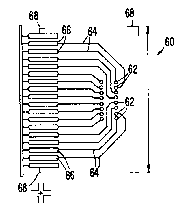
In Fig. 4, a pattern mask 60 is shown for a 16 pin DIP
having thermocouple pad terminal portions 62 for each
lead and equal width trace interconnections 64
connecting the thermocouple pad terminal portions 62
with signal monitoring connection portions 66. Of
course, it should be appreciated that the portions of
the mask 60 that are not within the positioning frame
corners 68, including the corner frames 68, would be
removed by an etchant, as noted above relative to the
process of making the thermocouple arrangements of the
present invention.
In Fig. S, a pattern mask 70 for a 16 pin DIP is
also shown. However, in this case, the thermocouple
pad terminal portions that are monitored via trace
interconnections 74 and connection portions 76 provide
a graduated circuit area ranging from terminal portions
72a, formed of lands of a small area/mass and
compa-able to those of Fig. 4, up to terminal portions
72b, which are formed as lands that have a large
area/mass. Since an increased circuit area produces
greater thermal loading, increased circuit areas will
lengthen the time it takes to heat a solder joint
thereat, Thus, a pattern as shown in Fig. 5 can be
utilized to emulate a circuit board having wide traces
,
. .
`:
2003202
or a g~ound plane attached to the pad. It is noted
that, i~ addltion to this technique, other techniques
can be used to slmulate ground planes (or other heat
sinXs) on or in a printed circuit board which may be a
sir.gle layer or multilayer board. For example, with
reference to Fig. 3, the diameter of the through hole
can be varied and/or the thickness of the hole wall
pla.ing 47 can be varied. As a result, electronic
assemblies and processes resulting in complex
temperature profiles can be emulated. For example,
many of the thermal characteristics of multilayer
prir.led circuit boards may be emulated by a much less
expensive double-sided board made according to the
present invention.
Fig. 6 shows a pattern mask 80 for a large,
surface mount component having 17 leads on each side,
but with terminal portions 82a for forming thermocouple
junctions at only three spaced locations at each side
(such as a~ the third, eighth and fifteenth lead), as
well as terminal portions 82b spaced 0.2 inches away
from the center of the row of terminal portions 82 at
each side. Such an arrangement allows a complex
p-ofile of temperatures of ~he component and
surrounding area to be obtained during various
processes. In this regard, while only 16 thermocouples
are shown in Fig. 6 (or for that matter in Figs. 4 and
5 as well), the number of thermocouples is limited only
by the amount of space available and the
interconnection capabilities via the lead traces 84 and
monitoring connection portions 86. Furthermore, the
use of _hermocouple arrangements of the type shown in
Fig. 6 is particularly advantageous with regard to the
evaluation of densely populated board assemblies to
determine the thermal effects transferred to components
that are not being directly operated on and can involve
monitoring of thermocouple junctions of adjacent
'
''
'
2003202
- 16 -
pacterns, not only those junctions of the pattern
pertainln~ to the component that is being directly
subjected to a thermally affecting process during a
particular emulation.
It should also be appreciated, from the foregoing,
that various permutations of (a) thermal mass
configurations, (b) heat source locations, and (c)
thermocouple iunction location can be created, in
accordance with the present invention, so as to be able
to emu'ate a wide assortment of printed circuit board
sizes, ~ypes, layouts and assembly configurations as
well as to evaluate a wide variety of
soldering/desoldering processes, or other types of
production, repair or rework operations requiring the
application of heat to a printed circuit board
arrangement.
Furthermore, while the printed circuit board
thermocouple arrangements in accordance with the
preser.t invention have all been described relative to
arrangements wherein the thermocouple junctions are
formed on an electrically insulative support that
simulates the effect experienced at various locations
on different types of printed circuit boards, it should
be appreciated that due to the use of conventional
printed circuit techniques to create the thermocouples,
other possibilities exist. For example, the printed
circuit thermocouples could be formed within a
simulated chip, wherein the number of printed circuit
thermocouples corresponds to the number of chip leads.
Alternatively, the number of printed circuit
thermocouples formed on the chip substrate, serving as
the electrically insulative support, could be less than
the number of chip leads, whereby some of the chip
leads may be connected to a heat source and others to
an output analyzer. In this way, temperature data
perteining to a production, repeir or rework operotion
:`
Z00320;~
beln~ performed on a printed circuit board can be
obtained in a manner reflecting the heat effects which
2. e directly experienced by an electronic component
ltself, thereby further expanding upon the ability to
train personnel, to develop, adjust and monitor any
~hermally affecting process, such as soldering, and to
evaluate process equipment in accordance with the
p~esent invention using, for example, an analyzer that
can store time and temperature curves, as described in
'he referenced U.S. Patent No. 4,224,744.
Those of ordinary skill in the art wi_l also
~ecognize that the materials described as examples for
use in consLruction of the present invention represent
only one possibility for which many substitutes are ~.
available. For example, instead of using a support
formed of a glass reinforced epoxy circuit board
substrate, ceramic, polyimide or polyimide/"
laminates may be used. Furthermore, instead of forming
T-type thermocouple junctions, K-type or J-type ~j3 i
thermocouple junctions could be formed using conductor
foils of chromel/alumel or iron/constantan,
respectively.
Mo-eover, it should be appreciated that a printed
circui~ thermocouple and the methods by which it is
made anc used as described above, for purposes such as
have beer. described above pertaining to the training of
personrel and evaluation of equipment, etc., represent
only a preferred int~nded application of the invention
on the part of the inventors which, by no means,
reflects the full utility of the invention. That is,
an array of thermocouples on a printed circuit
thermocouple arrangement, in accordance with the
present invention, could be utilized for almost any
situation wherein it would be desirable to obtain a
temperature profile of thermal effects. For example,
thermal insulation or heat loss effects could be
.~ .
:
.~ .
- 1 ~ - 200~202
evaluated ln a manner similar to that achievable by way
of inCrared photography, by coverins one or more
sLrfaces of a subject of study with a printed circuit
hermocou21e arrangement having suitable pattern(s) of
.hermocouples produced in accordance with the present ~ L/
invention. Furthermore, by using a flexible circuit'
board type substrate, such as one formed of polyimide
or polyimide/ ~ such a thermocouple arrangement ,~
could be easily applied to arcuate and other nonplanar ; 1
surfaces.
Still further, the method of fabricating-
~hermocouples via printed circuit technology in
accordance with the present invention even offers a
new, lower cost alternative to conventionally
constructed thermocouples for use as a substitute for
such standard thermocouples in any application for
which small individual thermocouples have been
heretofore used. In particular, a single large support
could be formed with a myriad of individual
thermocouple junctions in accordance with the present
invention, which support, with the thermocouples formed
~hereon, then being cut up into a corresponding number
of individual thermocouple elements, each of which has
a respe-tive one of thermocouple junctions thereon, at
a frac~ion of the cost associated with the existing
techniques for producing thermocouple elements. Here
again, the use of thin flexible substrate materials may
be advantageous.
Thus, since the present invention is susceptible
of numerous other changes and modifications as will be
apparent to those of ordinary skill in the art, the
present invention should not be considered to be
iimited to the details of the various embodiments shown
and described hereir., but rather should be viewed as
encompassing all such changes and modifications as are
within the scope of the apPended cla.ims.