Note: Descriptions are shown in the official language in which they were submitted.
~`` 2003207
1 28151-4
A RELAY RECEIVER
Background of the Invention
Field of the Invention
The present invention relates to a relay receiver for
performing a heterodyne relay to be used for a radio communication
system.
Brief DescriPtion of the Drawinqs
Figure 1 is an explanatory view of an example of
heterodyne relay system,
Figure 2 is a block diagram of the conventional prior
art,
Figures 3A and 3B are views for explaining the problem
of the prior art,
Figure 4 shows a principle block diagram of the present
invention,
Figure 5 shows a block diagram of the preferred
embodiment according to the present invention,
Figure 6 is a block diagram of the variable band
limiting portion and the band control portion in the preferred
embodiment of the present invention, and
Figures 7A and 7B are views for explaining an operation
of the preferred embodiment.
Description of the Related Art
Radio communication systems using microwaves, for
example, are widely used for transmission of telephone, television
and other signals. The field of digital communication technology
has recently been developing and the role of radio communication
systems has become increasingly important. The Integrated _I
~- 2003207
~ .
la 28151-4
Services Digital Network, or ISDN, is a good example.
Radio communication systems require a relay system to
perform long-distance communication. These systems generally use
a heterodyne relay, a detection relay or a direct relay.
The heterodyne relay system converts a received
microwave into an intermediate frequency band wave and then
reconverts the intermediate frequency band wave into a microwave
for transmission.
The detection relay system demodulates the received
microwave to provide a base band signal and
,_.,
2003Z0~
-- 2 --
then remodulates the base band signal into a microwave
for transmission.
The direct relay system amplifies the received
microwave, for example, in the frequency band of the
received microwave.
The system most used is the heterodyne relay
system because modulation distortion is not added
every time the relay is conducted.
Figure 1 shows the general structure of such a
heterodyne relay system. A relay station receives n
channel communication signals whose receiving
frequencies differ from each other by 80 MHz,
performs a heterodyne relay, and thereafter transmits
n channel communication signals whose frequencies also
respectively differ from each other by 80 MHz.
Note that the communication signal transmitted
from the upper station includes n channels with
central frequencies from f1 MHz to (f1 + 80(n-1)) MHz
every 80 MH z .
The above communication signals corresponding to
the respective channels are received by a common
receiving antenna, are divided into several parts by a
wave divider (not shown), and are input to the relay
receiving apparatus. In Figure 1, only the relay
receiver corresponding to a received signal with a
Z00~207
-- 3
central frequency f1 is shown, but the same structure
may be applied to the other central frequencies. This
relay receiver comprises a receiving frequency
converting portion 1, intermediate frequency amplifier
portion 2 and bandpass filter 3.
The receiving frequency converting portion 1
converts the frequency of the received signal with
central frequency f1 transmitted from the upper
station into an intermediate signal. The converted
output is amplified to reach a predetermined level by
intermediate frequency amplifying portion 2, which
includes an automatic gain control unit. The
amplified output is limited to a predetermined band by
bandpass filter 3 to be transmitted to a relay
transmitter. The bandpass filter performs waveforming
and noise removing functions. A relay transmitter
comprises transmitting frequency converting unit 41
and transmitting high frequency amplifier 42.
relay transmitter converts the output of the
- 20 bandpass filter 3 into transmission frequency f2 by
means of a transmission frequency converting unit 41.
This converted output is then amplified by a
transmission high frequency amplifier 42 to reach a
predetermined level. This amplified output is finally
mixed with the transmission signal of the other
2003207
frequency bands through a wave divider (not shown),
and is transmitted to the lower stage through a
transmission antenna.
The operation of the relay receiver and relay
transmitter recited above is similarly applied to the
communication signals corresponding to the other
central frequencies ~f1 + 80) MHz to (f1 + 80(n-1))
MHz.
In these systems, fading, caused, for example, by
rain, may occur in the transmission path, reducing the
receiving level of the received signal below a
predetermined level. When transmitting a digital
signal, it is thus necessary to prevent an increase in
the bit error ratio of received signal channels and
to reduce interference between adjacent channels as
much as possible.
Figure 2 shows a conventional relay receiver of
Figure 1. The receiving frequency converting portion
1 in Figure 1 comprises units 11 to 14 of Figure 2,
and the intermediate frequency amplifying portion 2 in
Figure 1 comprises units 21 to 28 of Figure 2.
Here, the transmission signal is a digital
modulation wave having a band width equal to clock
frequency fCK (which is called fCK hereinafter).
In Figure 2, a received signal with a central
200320~
-- 5
frequency f1 and a standard arriving level of minus
20dBm is received, for example, through the receiving
antenna, amplified by a receiving high frequency
amplifier 11, and then inputted to frequency
converter 13 through band pass filter 12 with a band
width of twice fCK- This band pass filter 12
performs a waveforming and a noise removing function.
In addition a receiving station signal is
inputted to the converter 13 by receiving station
oscillator 14. Thus, the input receiving signal is
then converted into an intermediate frequency fIF, and
this converted output is amplified by intermediate
frequency amplifier 21.
The amplified output is passed through a variable
attenuator~and is further amplified by intermediate
frequency amplifier 23. A portion of the output from
intermediate frequency amplifier 23 is detected by
detector 25. The detected voltage outputted from
detector 25 is applied to comparator 24, which
compares the above detected voltage with a standard
voltage V0. The amount of attenuation performed by
variable attenuator 22 is controlled based upon a gain
control signal outputted from the comparator so that
the difference between the detected voltage and
the standard voltage V0 becomes 0.
2003207
-- 6
Therefore, the output level from intermediate
frequency amplifier 23 is kept constant even if the
receiving level of the received signal varies.
The output of intermediate frequency amplifier 23
is inputted to intermediate frequency band pass filter
26, which limits the band width of the input signal to
the band width 1.5 times fCK- Intermediate frequency
band pass filter 26 performs the function of
waveformation and a noise removal.
The output of this intermediate frequency band
pass filter 26 is next transmitted to relay equalizer
27, which equalizes the relay distortion caused by
high frequency band pass filter 12 and intermediate
frequency band pass filter 26. The output of the
relay equalizer 27 is then further amplified by
intermediate frequency amplifier 28.
As is described above, the amplification
operation is conducted by a relay receiver. In a
system with this structure, if the receiving level of
the received signal with a central frequency f1 is at
a standard receiving level, the frequency
characteristic of the amplified signal outputted from
the relay receiver becomes as shown in Figure 3A. The
frequency characteristics of a transmitted signal with
a central frequency f2 outputted from the relay
~ 2003207
- 7 - 28151-4
receiver has the same characteristics obtained by replacing the
central frequency fIF in Figure 3A with f2. Therefore, the
transmitted signal has the band width of 50MHz.
If the receiving level of the received signal decreases
to a level of about 70dBm, for example, because of rain or an
occurrence of fading along its transmission path, the output of
the intermediate frequency amplifier 23 in Figure 2 is decreased
in a corresponding manner. In this case, comparator 24 is con-
trolled so that the amount of attenuation performed by variable
attenuator 24 becomes almost 0 in accordance with a gain control
signal.
As a result of the above operation, the total gain of
intermediate frequency amplifier 21, variable attenuator 22, and
intermediate frequency amplifier 23 increases and the output of
intermediate frequency amplifier 23 is kept constant even if the
receiving level changes.
However, the increase in gain causes the noise component
passing through intermediate frequency band pass filter 26 to in-
crease. The noise component, which has been either inputted to
receiving high frequency amplifier 11 or produced by receiving
high frequency amplifier 11, is superimposed on the
2003207
-- 8 --
received signal to relatively high level, and thus the
noise component superimposed on the received signal
cannot be disregarded. The resulting frequency
characteristic of the amplified signal outputted from
the relay receiver is shown in Figure 3B. Thus, the
frequency characteristic of the transmitted signal
outputted from the relay receiver is equal to the
characteristic obtained by replacing the central
frequency fIF in Figure 3B with f2.
As should be clear from the above explanation,
the frequency characteristics of the transmission
signal include the noise component designated by a
slanted line in Figure 3B, in addition to the real
transmission signal component having a band width of
plus or minus 25 MHz with respect to the central
frequency. In this case the noise component ranges
from plus or minus 40 MHz to plus or minus 50 MHz with
respect to the central frequency, thereby
substantially increasing the band width of the
transmission signal.
In the case where the receiving level of the
received signal is low, S/N (Signal vs. noise ratio)
of the transmitted signal decreases. Thus, during
transmission of a digital signal, for example, the
bit error ratio in a channel increases when the
200320~
transmission signal having the above frequency
characteristic is transmitted from the relay receiver
to the local station (not shown). This transmission
signal is then demodulated in the local station.
The band width of the transmission signal is
widened in the frequency range from plus or minus 40
MHz to plus or minus 50 MHz. Therefore the
transmission signal component in a local channel
overlaps with a transmission signal component of an
adjacent channel having a central frequency 80 MHz
from that of the local channel. The bit error ratio
of the adjacent channel is thus increased as in the
example shown in Figure 1. As a result, a plurality
of channels of the system go down and in the case of
a single suplementary line, that part of the system
which goes down cannot be saved.
As described above, the major problem with the
conventional relay receiver shown in Figure 2 is that
in the case of a decrease in the receiving level of
the receiving signal, the bit error ratio of the
channels relating to the receiving signal increases
upon transmission of a digital signal. The result is
inteference between adjacent channels.
In order to solve the above problem, for example,
consideration has been given to make the band width of
_ 20n3207
- 10 - 28151-4
intermediate frequency band pass filter 26 in Figure 2 narrow
enough only to allow the transmitted signal to pass. In the case
shown in Figure 3B, it may be considered that the intermediate
frequency band pass filter 26 is made to pass only the frequency
component of fIF plus or minus 25MHz. However, a filter with a
narrow band pass filter such as stated above degrades the ampli-
tude delay characteristic of a passing signal every time the pass-
ing signal is made to pass through the filter. Therefore, if the
characteristic of the above filter is made to have a uniformly
narrow band width, the amplitude delay characteristic of the
passing signal is degraded with an increase in the number of the
relaying operations, and the bit error ratio of the channel relat-
ing to the passing signal is increased in accordance with the
degradation in the amplitude delay characteristic of the passing
signal.
Summary of the Invention
The important objects of the present invention are to
suppress the bit error ratio of a channel relating to a received
signal and to suppress interference between adjacent channels,
even if the receiving level of a received signal decreases.
The present invention first comprises a receiving
frequency converting portion for converting a high
~.,
2003207
- 11 -
frCquency band received signal to an intermediate
frequency band signal.
The invention further comprises an intermediate
frequency amplifying portion for amplifying this
intermediate frequency band signal outputted from the
receiving frequency converting portion in accordance
with the state of later described gain control signal.
The invention further comprises an automatic gain
controller for outputting a gain control signal to
the intermediate frequency amplifying portion so that
the intermediate frequency amplifying portion can
output an amplified signal at a predetermined level,
based on the amplified signal outputted from the
intermediate frequency amplifying portion, even if
the arriving level of the received signals in the high
frequency band changes.
The invention further comprises a variable band
limiting portion for transmitting the amplified signal
outputted from the intermediate frequency amplifying
portion by limiting the amplified signal to a band
corresponding to the state of a band control signal.
The invention further comprises a band control
portion for outputting to the variable band limiting
portion a band control signal which limits the
amplified signal to a narrow band in accordance with
2003207
12 28151-4
a decrease in the arriving signal level of the high frequency band
received signal and based upon the gain control signal outputted
from the automatic gain control portion. The band control portion
outputs to the variable band control portion a band control signal
limiting the amplifying signal to a first band when the arriving
level of the received signal in the high frequency band is more
than a predetermined value. Conversely, the band control portion
outputs to the variable band control portion a band control signal
for limiting the amplifying signal to a second band narrower than
the first band when the arriving level of the received signal in
the high frequency band is less than the predetermined value.
As constructed above, the frequency band of the
amplifying signal is narrowed only when the receiving level of the
received signal is lowered. Therefore, the noise component is
controlled and the conventional increase in the bit error ratio of
the channel relating to the received signal is suppressed. The
frequency band width of the transmitted signal has thus been
prevented from expanding by the noise component and the
interference between adjacent channels is thereby decreased.
Other objects and characteristics of the present
invention will be easily understood by persons skilled in the art
based on the description of the preferred embodiment together with
the attached drawings.
Description of the Preferred Embodiment
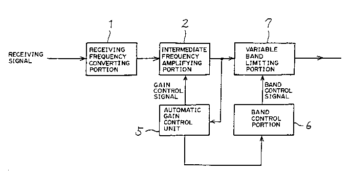
Figure 4 shows a block diagram of the principle
operation of the relay receiver according to the present
` 2003207
13 28151-4
invention.
In Figure 4, the received signal frequency converting
portion 1 has the same function as the
.~
- 2003207
- 14 -
portion 1 in Figure 1, namely to convert a high
frequency band received signal into an intermediate
frequency band signal.
Intermediate frequency amplifying portion 2 has
5 the same function as portion 2 in Figure 1, namely to
amplify the output of receiving frequency converting
portion 1 in accordance with the state of a gain
control signal inputted from automatic gain
controller 5.
Automatic gain controller 5 produces a gain
control signal for maintaining the above recited
amplified output at a predetermined level, using the
amplified output from intermediate frequency
amplifying portion 2, even if the arriving level
15 of the received signal in the high frequency band
changes.
Variable band limiting portion 7 limits the
frequency band of the amplified output from
intermediate frequency amplifying portion 2 to the
20 frequency band corresponding to the state of the band
control signal input from band control portion 6,
thereby outputting a communication signal subjected to
the band limitation.
Band control portion 6, utilizing a gain control
25 signal from automatic gain controller 5, outputs a
Z003207
-
- 15 -
band control signal in accordance with the arrival
level of a received signal to control variable band
limiting portion 7.
In the above structure, the band control portion
6 receives a gain control signal transmitted from
automatic gain controller 5 to intermediate frequency
amplifying portion 2, limits the band width of
variable band limiting portion 7 in accordance with
the gain control signal if the arriving signal level
of the received signal is low, and oppositely broadens
the band width of variable band limiting portion 7 if
the arriving signal level of the received signal is
high.
The frequency band of the amplified
communication signal is controlled to provide a narrow
band only when the receiving level of the received
signal decreases. In the case shown in Figure 3B,
the noise component shown by a slanted line is
supressed. Therefore, the bit error ratio of the
channel relating to the received signal is improved
and the frequency band width of the transmission
signal is prevented from expanding because of the
noise component. The interference between adjacent
channels is thereby decreased.
However, if the frequency band of the
2003207
- 16 -
communication signal is controlled to provide a narrow
band, the amplitude delay characteristic is degraded
as recited above. However, the decrease in a level of
the received signal does not occur along the entire
transmission paths, and thus it is unnecessary for
the relay receiver in all the relay stations to
provide a narrow frequency band for the communication
signal. In many relay stations where the arriving
levels of received signals are high, the relay
operation is conducted while keeping the frequency
band of the communication signal broad, thereby
providing little degradation of the amplitude delay
characteristics. In this case, therefore, the
present invention virtually avoids the prior-art
problem whereby the amplitude delay characteristic of
the communication signal degrades as the number of
the relays increases. In the present invention,
increase of the bit error ratio is suppressed to a
minimum.
Figure 5 shows a block diagram of the preferred
embodiment of the relay receiver according to the
present invention. Receiving high frequency amplifier
11, high frequency band pass filter 12, receiving
frequency converter 13 and receiving station
oscillator 14 perform the same function as portions 11
2003207
- 17 -
to 14, respectively, in Figure 2, thereby forming
receiving frequency converting portion 1 shown in
Figure 4.
Intermediate frequency amplifiers 21 and 23 and
5 varible attenuator 22 have the same function as
respective parts 21, 22 and 23 in Figure 2, thereby
forming intermediate frequency amplifying portion 2
shown in Figure 4. Detector 52 and comparator 51 form
automatic gain controller 5, as shown in Figure 4.
10 Intermediate frequency band pass filter 71, variable
band limiter 72, relay equalizer 73 and intermediate
frequency amplifier 74 form variable band limiting
portion 7 shown in Figure 4. Band control portion 6
in Figure 5 is the same as that in Figure 4.
Figure 6 shows a circuit structure of band
control portion 6 and variable band limiter 72 shown
in Figure 5. Here, Schmitt circuit 61, direct
amplifiers 62 to 65, subtractors 66, 68 and 69, and
adder 67 form band control portion 6 shown in Figure
20 5. The output of comparator 51 shown in Figure 5 is
applied to the Schmitt circuit 61 and the outputs of
Schmitt circuit 61 are respectively directed to
direct current amplifiers 62 to 65. The output
voltage of direct amplifier 64 is subtracted from
25 voltage V11 by subtractor 66. The output voltage of
2003Z07
- 18 -
direct amplifier 62 is added to voltage V12 by adder
67. The output voltage of direct amplifier 63 is
subtracted from voltage V11 by subtractor 68. The
output voltage of direct amplifier 65 is subtracted
5 from voltage V22 by subtractor 69. The output of
subtractor 68 is connected to resonator 723 in the
same manner that subtractor 66 is connected to
resonator 721. The output of subtractor 69 lS
connected to resonator 723 in the same manner that
10 adder 67 is connected to resonator 721. Resonators
721 and 723 and buffer amplifiers 722 and 724 form
variable band limiter 72 shown in Figure 5. Figure 6
shows only the structure of resonator 721, but
1~ . resonator ~ is of the same structure. The output
15 of intermediate frequency band pass filter 71 of
Figure 5 is connected to a first terminal of resistor
R1 and anode of pin diode D2. The output of
subtractor 66 is connected to the second terminal of
resistor R1. A cathode of pin diode D2 is inputted to
20 buffer amplifier 722 and is connected to an anode of
variable capacitor diode D1 and the first terminal of
coil L1. The cathode of variable capacitor diode D1
is connected to the first terminal of resistor R2 and
the first terminal of capacitor C. The second
25 terminal of resistor R2 is connected to the output of
2003207
-
- 19 -
adder 67. The second terminal of capacitor C and the
second terminal of coil L1 are grounded. The output
of buffer amplifier 722 is connected to an anode of
pin diode D2 in resonator 723 and the first terminal
of resistor R1. A cathode of pin diode D2 in
resonator 723 is connected to buffer amplifier 724.
The output of buffer amplifier 724 is inputted to
delay equalizer 73 shown in Figure 5.
An operation of the preferred emobodiment shown
in Figure 5 and 6 will be explained as follows.
The signal received by the receiving antenna (not
shown) and having a predetermined central frequency is
inputted to receiving frequency converter 13 through
receiving high frequency amplifier 11 and high
frequency band pass filter 12. The receiving station
signal from receiving station oscillator 14 is then
inputted to receiving frequency converter 13 and is
thereby converted into an intermediate frequency band
received signal.
The conversion output is amplified by
intermediate frequency amplifier 21, variable
attenuator 22 and intermediate frequency amplifier 23.
In this case, detector 52 and comparator 51 control
the amount of attenuation of variable attenuator 22 so
25 that the output of intermediate frequency amplifier
2003207
- 20 -
23 is at a predetermined level.
The predetermined level of the output from
intermediate frequency amplifier 23 is transmitted
through intermediate frequency band pass filter 71
having a predetermined value of band width, through
variable band limiter 72 controlled by band control
portion 6, and through delay equalizer 73. The
signal is further amplified by intermediate frequency
amplifier 74, thereby being transmitted to the
receiving side.
The operation of band control portion 6 and
variable band limiter 76 are most important to the
present invention and their operation will be
explained by referring to the structure shown in
Figure 6 and the explanatory view shown in Figure 7.
When the arriving signal level of the received signal
is higher than a predetermined value, the voltage from
comparator 51 in Figure 5 is low and thus the low
level output voltage from Schmitt circuit 61 in
Figure 6 is applied to subtractor 66 through direct
amplifier 64. The above low level voltage is
subtracted from the predetermined voltage value V11 in
subtractor 66 and the voltage value VD2 is thus
applied to pin diode D2 through resistor R1. In this
case, the voltage to be subtracted from predetermined
Z003207
-
- 21 -
voltage V11 by subtractor 66 is of a low level, and
thus voltage VD2 becomes relatively high. Therefore,
the diode resistance of pin diode D2 becomes small and
the Q value in resonator 721 becomes relatively low.
On the other hand, the low level output voltage
from Schmitt circuit 61 is applied to adder 67 through
direct amplifier 62. The above low level voltage is
added to the predetermined voltage value V12 in adder
67 and thus voltage VD1 is applied to a portion
connecting variable capacitance diode D1 and capacity
C through resistor R2. In this case, the voltage
value added to the predetermined voltage value V12 in
adder 67 is of a low level and thus the voltage value
VD1 becomes relatively low. Therefore, the resonance
frequency of the resonance circuit constituted by coil
L1, variable capacity diode D1 and capacity C becomes
relatively low in frequency fL. as shown in Figure 7A.
In accordance with the above operation, the
resonance characteristics shown by a' in Figure 7A can
be obtained in resonator 721.
The low level voltage obtained by direct
amplifier 63 through Schmitt circuit 61 is also
applied to subtractor 68. The above low level voltage
is subtracted from the predetermined voltage V11 in
subtractor 68 in a manner similar to that of
_ 2003207
- 22 -
subtractor 66. The output voltage of subtractor 68
controls resonator 723 in the same manner that the
output voltage of subtractor 66 controls resonator
721. Therefore, the Q value in resonator 723 becomes
5 relatively low in a similar manner to that in
resonator 721.
Further, a low level voltage supplied from
Schmitt circuit 61 through direct amplifier 65 is
applied to subtractor 69. The above low level voltage
10 is subtracted from the voltage V22 by subtractor 69
the voltage V22 differing from voltage V12 in adder 67
and, thereby providing a relatively high voltage
value. Therefore, the output voltage from subtractor
69 controls resonator 723 in the same manner that the
15 output voltage from adder 67 controls resonator 721.
In this case, the output voltage from subtractor 69 is
relatively high in an opposite manner to the output
voltage from adder 67. Therefore, resonance frequency
fH- determined by resonator 723 is relatively high as
20 shown in Figure 7A.
In accordance with the above operation, the
resonance characteristics shown by b' in Figure 7A can
be obtained in resonator 723. Resonators 721 and 723
are connected in a cascade manner through buffer
amplifiers 722 and 724, thereby providing a
Z003Z07
- 23 - -
characteristic wide band as shown by c' in Figure 7A.
Therefore, when the arriving signal level of the
received signal is high, the relay can be conducted
while the frequency band of the communication signal
kept wide.
In this case, the amount of attenuation in
variable attenuator 22 of Figure 5 is large and thus
the noise component is almost not included in the
frequency characteristic of the amplified output from
the intermediate frequency amplifier 23 as shown in
Figure 3A. Therefore, even if the relay is
conducted while the frequency band of the
communication signal is kept wide, a transmission
signal with a low bit error ratio, little inteference
between adjacent channels and whose amplitude delay
characteristics are not degraded can be obtained.
In contrast with the case recited above, when the
arriving signal level of the received signal is less
than a predetermined value, the output voltage from
comparator 51 in Figure 5 becomes large. Therefore, a
high level output voltage is applied to subtractor 66
through Schmitt circuit 61 and direct current
amplifier 64 shown in Figure 6. Subtractor 66
subtracts the above high level voltage from
predetermined voltage V11, thereby applying voltage
2003207
-
- 24 -
VD2 to pin diode D2 through resistor R1. In this
case, as the voltage to be subtracted from
predetermined voltage V11 in subtractor 66 is of a
high level, voltage VD2 becomes relatively low.
Therefore, the diode resistor of pin diode D2 becomes
large and the Q value in resonator 721 becomes
relatively high.
The high level voltage emerging from Schmitt
circuit 61 a high level output voltage is applied to
adder 67 through direct amplifier 62. The above high
level voltage is added to predetermined voltage V12 in
adder 67, thereby applying voltage VD1 to portion
connecting variable capacity diode D1 and capacity C
through resistor R2. In this case, as voltage added
to predetermined voltage V12 in adder 67 is of a high
level, voltage VD1 also becomes relatively high.
Therefore, the resonance frequency of the resonance
circuit constituted by coil L1, variable capacity
diode D1 and capacity C2 is shifted to a relatively
20 high frequency fL as shown in Figure 7B.
In accordance with the above operation, the
resonance characteristic shown by a in Figure 7B is
obtained in resonator 721.
On the other hand, the high level voltage is
25 applied to direct current amplifier 63 through Schmitt
200320~
-- Z5 --
circuit 61 and that is added to subtractor 68. In
subtractor 68, the above high level voltage is
subtracted from predetermined V11 in a manner similar
to that in subtractor 66. Output voltage from
5 subtractor 68 controls resonator 723 in the same
manner that the output voltage of subtractor 66
controls resonator 721. Therefore the Q value in
resonator 723 becomes relatively high in a manner
similar to that in resonator 721.
The high level voltage received through direct
current amplifier 65 from Schmitt circuit 61 is added
to subtractor 69. In subtractor 69, the above high
level voltage is subtracted from voltage V22 which is
different from that in adder 67, thereby outputting a
15 relatively low voltage value. The output voltage from
subtractor 69 controls resonator 723 in the same
manner that the output voltage from adder 67 controls
resonator 721. In this case, the output voltage from
subtractor 69 becomes relatively low in a manner
20 opposite to the output voltage from adder 67.
Therefore, resonance frequency fH determined by
resonator 723 becomes relatively low as shown by b in
Figure 7B.
In accordance with the above operation, the
25 resonance characteristic shown by b in Figure 7B is
Z003207
-
- 26 -
obtained in resonator 723. By connecting resonators
721 and 723 through buffer amplifiers 722 and 724
respectively in a cascade manner, the narrow band
characteristic shown by c in Figure 7B is provided.
5 Therefore, when the arriving signal level of the
received signal is low, the frequency band of the
communication signal is made narrow during a relay.
As the level of attenuation in variable
attenuator 22 in Figure 5 is small, both the noise
component and the communication signal component are
included in the frequency characteristic of the
amplified output of intermediate frequency amplifier
23 as shown by a slanted line in Figure 3B. The noise
component has a band width of plus or minus 40 MHz to
plus or minus 50 MHz with respect to the central
frequency, with the communication signal component
has a band width of plus or minus 25 MHz also with
respect to the central frequency. Accordingly, in
the case of the example shown in Figure 3B, the noise
component can be removed by adjusting the operation
characteristic of variable band limiter 72 shown in
Figure 6 such that resonance frequencies fL and fH
shown in Figure 7B become fO plus or minus 25 MHz,
where fO is a central frequency in an intermediate
frequency band of a communication signal.
2003207
In accordance with the above operation, a
transmission signal with a low bit error ratio and
with littlè interference between adjacent channels can
be obtained. As the above control is conducted only
in a relay station receiving a low-level of receiving
signal, it is unnecessary to narrow the frequency
band of a communication signal in all the relay
stations. Therefore, the conventional problem
wherein the amplitude delay characteristic of a
communication signal is increasingly degraded in
accordance with an increase of a number of the relays
is avoided. The present invention suppresses the bit
error ratio to a minimum.