Note: Descriptions are shown in the official language in which they were submitted.
2.1:1~3~
1 FIELD OF THE INVENTION
The invention relates -to a semiconduc-tor image sensor of which
the output signal may be controllably amplified. The invention also
relates to a sensor arrangement using such a semiconductor sensor.
BACKGROUND INFOR~IATION
Image sensors made of semiconductor elements are known in the art.
An article providing an over-view of such image sensors by
H. Herbst appears in "Elektronik-Praxis", No. 9, September 1978,
pages 12 to 14. The construction and use of such semiconductor
image sensors involves circuitry requiring an utmost integration
capability. Hence, great demands are made on the production
technology. This is especially true if the output signals which
are outputted by the sensor, for example after incidence of radi-
ation on the sensor, are only very small.
It is also known to provide a read-out electrode structure on
the surface of the image sensor such as a CCD-array. The read-
out electrode structure in the form of parallel strips is applied
to the sensor. Electrode configurations are disclosed in German
Patent Publication (DE) 3,817,153 Al, filed in the Federal
Republic of Germany on: ~ay 19, 1988, which is not a prior pub-
lication.
European Patent Publication 0,309,927 (Laucht et al.), published
on April 6, 1989, discloses an image distance sensor that could
be used in conjunction with the present invention. The disclo-
sure of said European Patent Publication is incorporated herein
by reference.
),t3~
It is known to use image sensors in various image detection
systems, for example, in dis-tance measuring and proximity
warning systems as disclosed, for example, in German Patent Publica-
tion (DE) 3,640,449 Cl, published June 30, 1988. Such sensors are also used
in an automatic control and guidance system for motor vehicles
travelling on a highway while maintaining a prescribed rela-
tive spacing between -the vehicles travelling in a column as
described in "Funkschau" Nr. 14/1988, page 42 pp. Use in a
similar automa-tic vehicle guidance system known as "Prometheus"
described in "Bild der Wissenschaft", Nr. 10/1988, pages 134,
135 is also possible.
OBJECTS OF T~IE INVENTION
In view of the foregoing it is the aim of the invention to
achieve the following objects singly or in combinationo
to construct a semiconductor image sensor having
an improved signal to noise ratio to provide an increased
output signal compared to prior art image sensors;
to control the signal amplification in such an image
sensor by simple means and in a simple manner; and
to construct such an image sensor in an economical
manner employing generally known methods of semiconductor
doping, masking, etching, and related techniques.
~OC~36~
SUMMARY OF THE INVENTION
The above objects have been achieved according to the invention
by a semiconductor image sensor, particularly having a CCD-
structure,arranged as a one--dimensional linear array or as a
two-dimensional surface array with a parallel or serial read-
out, and with an avalanche diode arranged on one side for
amplifying a photo-current produced by a light input, wherein
a space charge is produced in the neighboring or connecting
semiconductor zone, wherein charge carriers are transported
to a CCD-read-out structure for outputting a contrast or dis-
tance image by said CCD-read-out structure arranged on the
other side of the semiconductor, and wherein optical control
is provided by introducing pulsed light, especially pulsed
laser light into said semiconductor zone in which said space
charge has been produced.
Thus, the present image sensor is essentially a photosensitive
semiconductor element such as a CCD-element in which the signal
may be amplified by employing an avalanche effect in a surfacial
avalanche diode element of the semiconductor. The avalanche
effect and therewith the amplification, can be optically con-
trolled simply by appropriately illuminating the image sensor
with a control laser beam which may be pulsed in a controlled
manner. By using the avalanche effect of a surfacial avalanche
diode on a CCD-sensor, the sensitivity and amplification of
the sensor element is increased by a factor of approximately
one hundred.
~i~(3~
1 The controllably amplifying image sensor according to the
invention may be advantageously used as a shutter or sampler
for video images, or as a receiver in a motor vehicle dis-
tance measuring system and proximity warning system, or as
a receiver in an automatic motor vehicle guidance system em-
ploying a guide track as part of an integrated services data
network in which vehicles keep a defined mutual distance.
BRIEF FIG~RE DESCRIPTION
In order that the invention may be clearly understood, it
will now be described, by way of example, with reference to
the accompanying drawings, wherein:
Fig. 1 is a schematic perspective view of the
essential elements of an optical sensor arrangement
using the present sensor, for example in a
motor vehicle for providing informationregarding
obstacles on the road ahead;
Fig. 2 is a schematic perspective view similar to
the embodiment of the invention as shown in
Fig. 1, wherein the optical sensor functions
as a shutter controlled by a pulsed laser
beam;
Fig. 3 is a cross-sectional view through the CCD-
optical sensor for operating as a receiver
element in the arrangement of Fig. 2;
~003~
1 Fig. 4 shows a cross-sectlon similar to that of
Fig. 3, but through a modified embodiment
of a CCD-optical sensor also for operating
as a receiver element;
Fig. 5 is a cross-section through a further varia-
tion of a CCD-optical sensor element;
Fig. 6 is a schematic perspective view ofareceiver ar-
rangementincorporating the CCD-optical sensor
element of Fig. 5;
Fig. 7 is a cross-section through a variation of
an optical sensor or receiver element similar
to that of Fig. 5 which can be used in the
arrangement of Fig. 6;
Fig. 8 is a pulse diagram showing signal sequences or
pulse trains for controlling an optical sensoror
receiver element of Fig. 7; and
Fig. 9 is a block circuit diagram for operating
an optically controllable image sensor ac-
cording to the invention in a system for
providing,to a driver of a vehicle,informa-
tion regarding other vehicles or obstacles
on the road ahead.
1 DETAILED DESCRIPTION OF PREFERRED EXAMPLE EMBODIMENTS AND
OF THE BEST ~iODE GF THE INVENTION
Fig. 1 schema-tically shows an optical sensor arrangement for
sensing images incorporating an image sensor according to
the invention used, for example, in a motor vehicle guidance
and control system. In -the arrangement a laser source 1
carried by each vehicle par-ticipating in the system,transmits
an illuminating laser beam 1' through transmitting optics 2
in the travel direction to illuminate an image of the road
scene ahead. r~he road scene is not shown, but lies to the
right of Fig. 1. Reflected light 4' returns from the image
scene through receiving optics 4 and impinges on an image
receiver or optical sensor embodied as a flat planar semicon-
ductor CCD-array 3. A received image display 6 is shown
schematically to illustrate the output from the optical sen-
sor CCD-array 3 viewing forward from a motor vehicle.
The vehicle guidance and control system which as such is not
part of the invention, may simultaneously project, receive,
and evaluate laser beams for distance measurements to obstruc-
tions or other travelling vehicles in front of the motorvehicle carrying the present arrangement. Means for evaluat-
ing the image signals received from the present CCD-sensor 3
including evaluation circuitry are known as such and are there-
fore not shown and described in detail herein, merely the
display 6 is shown on a reduced scale.
2~103~
l As further indicated in Fig. l, the image receiver according
to the invention includes an avalanche diode 5 on one surface
of the CCD-sensor 3. The avalanche diode 5 is attached to
the semiconductor which receives the incident laser radiation.
This feature is achieved by implanting or doping an appropriate
layer on the backside of a CCD-chip. The various materials
and manufacturing techniques for achieving the implanting
or doping are known.
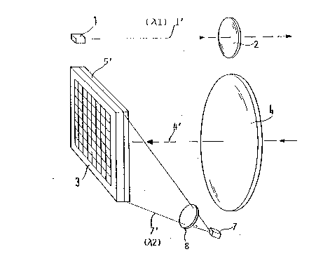
Fig. 2 shows an arrangement according to the invention, similar
to that of Fig. 1, but further including a controllable shut-
ter 5' and means for controlling or gating the shutter 5'.
These gating means include a semiconductor laser 7 operating
as a gating or control laser 7 whieh projeets a gating or
eontrol beam 7' through control optics 8 to impinge upon the
CCD-sensor 3. The laser 7 operates at a gating wave length ~2,
preferably between 1400 nm and 1800 nm. In choosing the gating
wave length ~ 2 it is important that ~ 2 is sufficiently
differentiable from the wave length ~ 1 to be measured and
projeeted by the illuminating laser l, for example, at a wave
length of between 800 and 950 nm whieh is typieal for semieon-
duetor lasers used for distanee measurement. The eontrollable
optie shutter 5' is operated in a gating mode instead of the
typieal CCD semieonduetor element arrangement shown in Fig. l.
Fig. 8, to be deseribed in more detail below, illustrates the
gating control of the semieonduetor laser 7 emitting gating
light pulses having a wave length ~ 2.
-- 8
~()03~,~3
1 Eig. 3 is a cross-sectional view showing the geometric arrange-
ment of the receiver or optical CCD-sensor 3 of Fig. 2,
especially including the optical shutter 5' for an exposure
control. The general semiconductor layer structure is p-n-p.
The semiconductor sandwich includes a bottom layer 13 of
p-Si, a middle layer 12 of n-Si, and a top layer 11 of p-Si.
Read-out electrodes 9 are attached to the top or back elec-
trode 10. As shown, both the image beam 4' and the control
beam 7' are incident on the bottom or front electrode func-
tioning as a shutter 5' which includes elements 14 and 15
which are respectively sensitive or transparent or excitable
at the wave lengths ~1 of the image beam within the range
of 800 to 950 nm and ~2 of the control or gating beam at
1400 nm. A voltage of up to -300 V is applied between ground,
electrode 10, and the layer 13. A voltage of approximately
+5 V is applied between the middle n-Si layer 12 and ground
10. Application of the -300 Volts triggers the reverse
avalanche breakdown, so that the incident radiation can pass
through the serniconductcr structure thereby generating irnage
signals which may be read out at the electrodes 9 in a manner
described, for example, in the German Patent Publication (DE)
3,817,153 Al or in the manner shown in the block circuit
diagram of Fis. 9.
Fig. 4 shows an embodiment of an optical sensor in which
the avalanche effect does not occur on the surface or back
side of the CCD which receives the incident radiation, but
rather the avalanche effect occurs laterally, or in other
words, horizontally in side-by-side fashion as shown in Fig. 4.
~on3~3
l ~ transparent or semitransparent subs-trate 22 carries a high
ohmic or highly resistive n-Si layer 21 on which a CCD-struc-
ture is applied in a horizontally and sectionally seen middle
area, including p-Si layer regions l9 and an SiO2 region 20,
the latter reaching into the n-Si layer 21 as shown at 20'.
The regions 20 and 20' are also p-Si regions and are trans-
parent SiO2. Specifically, the cone-shaped region 20' be-
tween adjacent p-Si regions 19 partially penetrates into or
is embedded in the n-Si layer 21. The CCD-structure on the
risht side of Fig. 4 comprising the p-Si layer 19 includes
a read-out structure 18 especially an electrode structure 18
made of aluminum electrodes or the like. On the left side
of Fig. 4, a thin layer 17 of transparent material such as
gold, is applied and preferably one or mGre filter layers 16a
are applied over the conductor layer 17. The filter layer 16a
selectively transmits the incident image beam 4' at the wave
length ~1. A further filter layer 16b may be applied over
the transparent SiO2 region 20 to selectively transmit the
control or gating beam 7' at the wave length A 2.
Fig. 5 shows a cross-section through a further embodiment
of an optically controllable image sensor according to the
invention, wherein the image beam 4' and the control beam 7'
are incident on the semiconductor sensor element from opposite
sides. A thin transparent layer 28 of, for example, gold,
forms the cover electrode of the semiconductor package on
the side of incidence of the image beam 4'. The gold layer
or electrode 28 is applied to a layer made up of regions
27a, 27b of p-Si laterally separated from one another by
-- 10 --
~uo~
1 regions 29 of SiO2. Next in the sandwich arrangement is
a layer 26 of high ohmic or highly resistive n-Si and next
is a layer 25 of continuous p-Si. Next in the arrangement
is a continuous top layer 24 of transparent or semi-trans-
parent material, preferably of SiO2 onto which read-out elec-
trodes 23 of aluminum or gold or the like are deposited in
the form of parallel strips by means of masking techniques,
or especially photolithographic techniques. These electrodes
23 may have the shape as described in the above mentioned
German Patent Publication (DE) 3,817,153 Al.
In Fis. 5 the control or gating light beam 7' enters the
semiconductor element from above through the SiO2 layer 24
to generate a space charge in the semiconductor element.
It is advantageous if the various elements, especially the
read-out electrode strips 23,are arranged so that the inci-
dent image beam 4' does not enter into the semiconductor
immediately vertically below the control light beam 7', but
rather displaced laterally or horizontally therefrom as~ shown
in Fig. 5.
Fig. 6 shows an arrangement which could for example, use
the semiconductor image sensor element shown in detail in
Fig. 5 or other sensor elements of the invention which receive
the control light beam 7' and the image light beam 4' on
opposite sides. The system shown in the embodiment of Fig. 6
is especially suitable for use in an automatic motor vehicle
control and guidance system for maintaining a prescribed
relative distance between vehicles following one another
q2~00~3~
1 in a convoy, see, for example the above mentioned "Funkschau"
Nr. 14/198g, page 42. An illuminating laser 1 again projects
a laser beam 1' a-t the wave length Al, which is, for example,
between 800 and 950 nm or any other wave length suitable
for the purpose, whereby the beam 1' is reflected by the
scene and returns to the optical sensor 3 as the image beam 4'
through the receiver optics 4. The control or gating or
sampling beam 7' generated by the control or gating laser 7
illuminates the image sensor 3 in the form of a CCD-array
on the side opposite to the side on which the image beam 4'
is incident.
Fig. 7 is a cross-section through another sensor element
or CCD-array 3 which can be used in the arrangement of Fig. 6,
which is somewhat similar to the sensor of Fig. 5 in that
the image beam 4' and the control beam 7' illuminate the
sensor 3 from opposite sides. However, in the embodiment
of Fig. 7, the incident image beam 4' illuminates the CCD-
element from above on the side carrying the read-out elec-
trodes 30. In Fig. 5 the control beam 7' enters on the side
carrying the read-out electrodes 23. The CCD-sensor structure
in Fig. 7 includes a p-Si layer 31, a middle n-Si layer 32,
and a bottom p-Si layer 33. The control beam 7' typically
having a wave length of 1400 nm illuminates the CCD-element
from below as shown.
Fig. 8 is a diagram showing the signal or pulse sequences
involved in the operation of the image sensor 3 according
to the invention. The upper part of Fig. 8 shows the
- 12 -
Z003~3
l radiation having the wave length ~l to be measured as a func-
tion of time on the abscissa with an illumination intensity up
to approximately 10,000 lux for control voltage pulses of
- 300 V and for -280 V applied across the image sensor to car-
ry out the optical control or gating of the image sensor as
described above.
The lower part of the diagram of Fig. 8 shows the current flow
on the ordinate in the form of timed pulses at a sampling time
of the control or gating or sampling laser pulses limited in
duration to approximately 10 ns or shorter. Other sampling
pulse forms or modulations are possible, e.g. pulse code modu-
lation or pulse duration modulation may be applied to the sam-
pling beam 7'.
Fig. 9 shows a block circuit diagram of the entire system es-
pecially employed in a motor vehicle control and guidance sys-
tem as described above. A laser control 34 activates an illu-
minating laser l which illuminates the subject image through a
lens or transmitting optics 2. A reflected beam is received
through receiving optics 4 and impinges on a controllable image
sensor 3 according to the invention. A time clocking device 37
activates a gate generator 38 which simultaneously provides
control impulses to the laser control 34 and to the gating or
sampling laser 7 which transmits pulses to the controllable
image sensor 3. The gate generator 38 further activates a
CCD-read-out unit 40 which receives the image information from
the controllable image sensor 3 to produce a distance image
signal 6' for showing the scene 6.
- 13 -
~003~,R3
l The above description shows that a flat planar image sensor
has been constructed having a high sensitivity and also a
capability of controlling the sensor in very short time
intervals in the ns range, especially less than lO ns, for
example 5 ns. This capability of the image sensor according
to the invention enables the sensor to effectively operate
as an electronic shutter for a CCD-camera or as a sensor
in a motor vehicle guidance system as described above. Accord-
ing to the invention, the sensitivity has been increased
or the signal has been amplified by a factor of approximately
lO0 due to the special utilization of the avalanche effect.
The amplification factor may be adjusted by varying the aval~
anche voltage applied across the semiconductor element.
The sensor according to the invention may be advantageously
used in a spacing warning system and distance measurement
system using a laser according to, for example, German Patent
Pubication (DE) 3,640,449 C1. The sensor according to the
invention may further be used in an automatic guidance system
"Prometheus" as described, for example, in "Bild der Wissen-
~0 schaft" 10/1988, page 134.
Although the invention has been described with referenceto specific example embodiments, it will be appreciated,
that it is intended to cover all modifications and equiva-
lents within the scope of the appended claims.
- 14 -