Note: Descriptions are shown in the official language in which they were submitted.
797'7
~~~~~~~~~a
Title: INTEGRATED OPTIC PRTNT HEAD
Technical field of the Invention
The present invention in general relates to
laser print head structures and, in particular, to an
integrated optics laser print head which utilizes
integrated waveguides.
Background of the Invention
There are a number of problems in
manufacturing laser print heads which are fabricated
from semiconductor lasers. One problem occurs because
there is a limit on how close semiconductor lasers may
be to each other on a substrate while still being
independently addressable. Specifically, the distance
between semiconductor lasers fabricated on the same
substrate should be greater than approximately 100
microns for them to be independently addressable. If
the semiconductor lasers are disposed any closer to each
other than that, interference between adjacent lasers
occurs when one of them is excited. For that reason,
most attempts in the art at fabricating laser print
heads have used isolated semiconductor lasers.
Another problem occurs when attempting to
couple light from semiconductor lasers to small closely
spaced pixel areas. Specifically, optical fiber
elements which have previously been used in the art are
incapable of achieving the close proximity of the
_1_
~~3~~'~CD~~
independent output pixels required for a laser print
head.
As a result, there is a need in the art for a
laser print head structure which: (1) has semiconductor
lasers disposed in close proximity to one another while
still being individually addressable; (2) has light
transmission means which transmits light from the
individual, isolated semiconductor lasers to provide
output pixels having spacinc~s between adjacent pixels
which are substantially smaller than the spacings
between adjacent semiconductor lasers; and (3) has light
transmission means with low loss due to absorption or
scattering and low crosstalk among its several channels.
Summarv of the Invention
Embodiments of the present invention
advantageously provide integrated optics laser print
heads which comprises an array of independently driven
semiconductor lasers disposed on a common substrate with
their outputs coupled to an integrated waveguide
structure. The integrated waveguide structure comprises
a multiplicity of low-loss waveguides, each one of which
is coupled to a laser at its input end and outputs a
substantial portion of the coupled radiation at its
output end. The input ends of the waveguides are spaced
far apart in accordance with the spacing of the lasers
while their output ends are spaced close together in
accordance with the pixel requirements of the laser
printer. In addition there is low crosstalk among the
waveguides.
As noted above, the inventive integrated
optics lasez~;rprint head comprises an array of
independently driven semiconductor lasers disposed on a
common substrate. Because of this, the problem of
aligning individual lasers and individual waveguides in
the integrated waveguide structure is reduced
substantially when compared to the problem that would
_2_
exist if the lasers were disposed on a multiplicity of
substrates.
Further, the inventive integrated optics laser
print head comprises an integrated waveguide structure
comprised of a multiplicity of waveguides, each one of
which is coupled to a laser at its input end and outputs
a substantial portion of the coupled radiation at its
output end. Embodiments of t:he integrated waveguide
structure come in two categories. One category is
useful in applications where the optical density change
of a photosensitive medium de:p~nds on the amount of
light to which it is exposed. Thus, in order to
maintain a uniform exposure in such applications, the
amount of light output from each waveguide of the
integrated waveguide structure is required to be
substantially equal. Another category finds utility in
applications where the exposure of the photosensitive
medium operates according to a threshold phenomenon.
Thus, in order to maintain a uniform exposure in such
applications, the amount of light output from each
waveguide of the integrated waveguide structure is
required merely to be greater than a predetermined
threshold amount.
In one embodiment of the present
invention directed to producing a substantially equal
amount of output light from the various waveguides, the
waveguides have different losses and the amount of bias
applied to the lasers is varied in order to compensate
for the different losses among the various waveguides.
In another embodiment of the present invention directed
to producing a substantially equal amount of output.
light from the various waveguides, lasers are biased at
substantially the same level and the waveguides have
substantially equal loss in order to obtain
substantially the same light output from each. Here,
the term substantially equal loss means that the losses
among the various waveguides is equal within the
-3-
sensitivity tolerance limits of the photosensitive
medium which is exposed to the outputs from the
waveguides, i.e., if the photosensitive medium cannot
detect differences of less than, for example, .3 dB,
'then the losses of the waveguides need only be within .3
dB of each other to be substantially equal.
~Ievertholess, in order to have substanvially equal loss
for each waveguide, the waveguides preferably have
substantially equal lengths.
In an embodiment of the present invention
directed to producing an amount of output light which is
above a predetermined threshold, the waveguides may have
an arbitrary loss as long the light output from each is
above the predetermined threshold.
In addition to the above°described
considerations, there are other requirements which must
be considered in designing the integrated waveguide
structure of the inventive integrated optics laser print
head. A first requirement is to maintain crosstalk
among the waveguides at a low level; a second
requirement is to reduce the loss in the waveguides to
small values; and a third requirement is to fabricate
the input regions of the waveguides.so they are
substantially parallel to each other and to fabricate
the output regions of the waveguides so they are
substantially parallel to each other to provide that
coupling light into and out of the waveguides is easier
and more efficient.
The first, second and third requirements are
satisfied in a preferred embodiment of the present
invention by-forming them in the shape of an "S." In
such an "S" shaped integrated waveguide structure
crosstalk is a concern in the neighborhood of the output
regions of the waveguides because there the waveguides
are sufficiently close enough so that light radiated
from one waveguide may be captured by adjacent
waveguides. This occurs because it is only at the
°
output region of the waveguides that the waveguides need
be close enough to each other to provide the output
pixel spacing required for the laser printer. Thus,
because crosstalk between two waveguides is proportional
to the length over which the two waveguides are in close
proximity, the "S" shaped embodiment is designed so that
the neighborhood where the output regions of the
waveguides are close to each other is short enough to
limit crosstalk to be at a low level. Further, in the
preferred "S" shaped embodiment, the input regions of
the waveguides are all parallel and the output regions
are also all parallel, Still further, the "S" shaped
waveguides have only two bends, each of which is
designed to limit the amount of loss due to radiation.
Yet still further, the °'S" shaped waveguides are
designed to have substantially the same length.
Integrated waveguide structures have been
fabricated, for example, thermally-assisted, Ag-Na
exchanged, waveguide structures in soda-lime-silicate
glass. with propagation losses of approximately .7
dB/cm. This propagation loss is used to determine a
design limit on the length differential among the
individual waveguides of the integrated structure. For
example, if the 'output medium upon which the output
light from such a waveguide structure is focused can
tolerate a loss differential as large as .25 dB, then
the length differential for the waveguides can be as
great as .3 cm.
Notwithstanding the above, one further
consideration pertaining to the inventive laser print
head is related to the method of fabrication of the
waveguides. This further consideration arises because
of the need to fabricate groups of.waveguides having
small separations between neighboring waveguides,
especially in the neighborhood of the output ends
thereof. A,s a result, a preferred embodiment of the
present invention is fabricated using "field-assisted
-5-
CA 02004046 2000-05-23
63356-1757
ion-exchange" to form the waveguides because this method has an
inherent aversion towards diffusion into the low index optical
separation region between the waveguides. As a result, loss
and crosstalk will be minimized. In addition, in a preferred
embodiment, the waveguides are buried in order to reduce light
loss due to scattering from surface imperfections on the
surface of the integrated waveguide structure.
Thus, preferred embodiments of the inventive
integrated print head comprise "S" shaped integrated waveguide
structures where: (1) individual waveguides have substantially
the length and, thereby, substantially the same loss; (2) the
portion of the waveguide structure where the individual
waveguides are disposed close to each other in the
neighbourhood of the output regions thereof is as short as
possible in order to minimize crosstalk; (3) the other regions
of the integrated waveguide structure have the individual
waveguides disposed far enough away from each other so that
crosstalk is virtually eliminated; (4) the individual
waveguides are fabricated using "field-assisted ion-exchange";
and (5) the waveguides are buried.
The invention may be summarized as a print head
having a predetermined spacing between outputs, which print
head comprises: a multiplicity of independently excitable light
sources fabricated on a first substrate; and an integrated
waveguide structure comprising a multiplicity of waveguides
having an input end and an output end fabricated on a second
substrate, said first and second substrates being aligned so
that light from said light sources is coupled into the input
end of said waveguides, said waveguides having a shape which
comprises a first bend disposed after said input end and a
6
CA 02004046 2000-05-23
63356-1757
second bend disposed after said first bend and before said
output end to form a substantially "S" shape, said waveguides
being disposed so that the distance between adjacent waveguides
is substantially equal to a predetermined spacing after said
second bend and the distance between adjacent waveguides is
substantially greater than another predetermined spacing at all
other portions.
Brief Description of the Drawin
The present invention may be understood by
considering the following detailed description together with
accompanying Figure 1 which shows, in pictorial form, an
embodiment of the inventive integrated optics laser print head.
Detailed Description
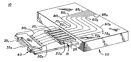
FIG. 1 shows a preferred embodiment of inventive
integrated optics laser print head designated at 10. An array
15 of semiconductor lasers 201 to 20n fabricated on a substrate
25. The center-to-center spacing between adjacent ones of
lasers 201 to 20n is defined lithographically and is
sufficiently large that the lasers are individually
addressable. For example,
6a
it was determined that GaAs/AlGaAs lasers emitting
radiation at a wavelength of approximately .8 microns
can be placed at a minimum center-to-center spacing of
approximately 100 microns and still be independently
addressable. Thus, a typica:L embodiment of array 15
comprises photolithographically defined stripes having
center-to-center spacings bei~ween adjacent stripes in
the range between 100 to 500 microns and a stripe width
of approximately 5-15 microns. Substrate 25, far
example, GaAs, has a thickness in the range between 75
to 150 microns. A thickness at the low end of the
range, for example, 75 microns, is preferred because
this facilitates the ability to independently drive
individual lasers 201 to 20n. Substrate 25 is then
bonded by, for example, indium solder for good thermal
conduction, to a cleaved diamond substrate, not shown,
having a minimum thickness of approximately 250 microns.
The cleaved diamond substrate should achieve a
substantially perpendicular edge with substrate 25 and
substrate 25 should not protrude over the edge of the
diamond substrate nor be back from the edge by more than
approximately 5 microns. In addition, the diamond
substrate is bonded by methods well known to those of
ordinary skill in the art to a thermoelectric cooler,
not shown. Although laser array 15 is shown to be a
GaAs/AlGaAs heterostructure laser, other materials and
constructions known in the art may also be used. Shown
in Fig. 1 is the embodiment with the epitaxial layers of
the laser diodes on the upper surface of the GaAs
substrate. The laser diode array can be inverted to
have the epitaxial layer nearer the heat sink thereby
more readily conducting the heat away to allow higher
output values from the diodes.
Lasers 201 to 20n are addressed by means of
electric signals applied to pins 351 to 35n of array 40.
Pins 351 to 35n are then connected to lasers 201 to 20n
by leads 30.1 to 30n, which are bonded to lasers 201 to
-7-
20n, respectively. The electric signals for exciting
the individual lasers are generated by means (not shown)
which are well known in the art.
Array 15 is affixed to integrated waveguide
structure 50 so that radiation output from lasers 201 to
20n is coupled into waveguides 601 to 60n, respectively.
A typical output cross-sectional area for lasers 201 to
20n is 5 by 2 micrometers. Array 15 is aligned in
x, y, z positions to within .1 micron and is also
aligned angularly and affixed in place by, for example,
temperature stable indium solder or epoxy. As one can
readily appreciate from FIG. 1, the ability to align
lasers 201 to 20n with waveguides 601 to Eon,
respectively, is substantially enhanced because lasers
201 to 20n are fabricated on common substrate 25 and
have lithographically defined center to center spacing
equal to that of the guides.
In a preferred embodiment, waveguides 601 to
60n have shapes which meet the following constraints:
(1) input regions 701 to 70n are substantially parallel
to each other and to the orientation of the stripes of
lasers 201 to 20n, respectively, to promote efficient
coupling thereinto of light output by lasers 201 to 20n;
(2) output regions 851 to 85n are substantially parallel
to each other to promote efficent coupling of emerging
light for transmittance to the media to be illuminated
(3) waveguides 601 to 60n have substantially the same
loss and, therefore, substantially the same length; and
(4) the portions of waveguide structure 50 where
individual waveguides 601 to 60n are disposed close to
each other is short to minimize crosstalk.
The amount by which the loss in waveguides 601
to 60n can differ from one another is determined by the
type of photosensitive medium which is exposed to the
outputs from the waveguides. Far example, if the medium
is a threshold medium, i.e., one requiring a certain
level of light to cause an effect, the waveguide loss is
_g-
~'~ ~ ~' ~?
constrained to be small enough so that the output light
is above the predetermined threshold. In such a case,
any length differential among the waveguides can be
tolerated as long as the light output does not fall
below the threshold. On the other hand, if the medium
sensitivity to light depends on the intensity in, for
example, a linear fashion instead of in a threshold
fashion, then the particular design of the embodiment
must provide substantially equal loss for the waveguides
if the laser outputs are substantially equal. However,
in the design sense, the team substantially equal loss
means that the loss differential among the various
waveguides be equal within the sensitivity -tolerance
limits of the photosensitive medium which is exposed to
the outputs from the waveguides. Thus, if the
photosensitive medium cannot detect loss differences of
less than, for example, .3 dB, then the losses of the
waveguides need only be within .3 dB of each other to be
substantially equal. For this case then with a
waveguide material having a propagation loss of
approximately 1.0 dB/cm, the requirement of
substantially equal loss will be satisfied if the length
differential among the waveguides is less than .3 cm.
Further, this defines the requirement that the
individual waveguides have substantially the same
length. Furthermore, laser diode bias can be adjusted
to compensate for differences in propagation losses.
waveguides 601 to 60n of integrated waveguide
structure 50 are "S" shaped waveguides arid have input
regions 701 to 70n, respectively, first bends 751 to
75n, respectively, second bends 801 to,80n,
respectively, and output regions 851 to 85n,
respectively. A typical cross-sectional area of input
regions 701 to 70n is 10 by 5 micrometers to ensure.
substantial coupling between lasers 201 to 20n and
waveguides 601 to Eon, respectively. Further, input
regions 701 to 70n are also preferably parallel to each
_g_
other and to the orientation of the stripes of lasers
201 to 20n, respectively, to enhance coupling
therebetween. Because waveguides 601 to 60n are "S"
shaped, they may be designed so thate (1) each waveguide
has substantially the same length from input end to
output end; (2) the neighborhood where the waveguides
are close to each other near the output and is as s.'zort
as possible in order to eliminate cross-talk. and (3)
input regions 701 to 70n are substantially parallel to
each other and output regions 851 to 85n are
substantially parallel to each other.
In a typical print head application for the
inventive integrated optics laser print head the output
beams should be approximately 14 microns apart. As a
result, the center-to-center spacing of waveguide output
regions 851 to 85n should also be approximately 14
microns. Because of the resulting close proximity of
waveguides 601 to 60n in output regions 851 to 85n, it
is necessary to make the neighborhood of these output
regions where the waveguides are closely adjacent to
each other as small as possible in order to minimize
crosstalk, i.e., the phenomenon where light radiated
from one waveguide is absorbed by another. Further, the
waveguides should be spaced fax enough apart from each
other in the other regions of waveguide structure 50
that crosstalk is no problem at all.
In FIG. 1, waveguides 601 to Eon all have
substantially the same length and have an approximate
10 micrometer width and an approximate 5 micrometer
depth in soda-lime-silicate glass. The waveguides can
be formed by any one of a number of methods known in the
art such as, as will be explained in detail below, by an
Ag-Na or a K-Na ion-exchange process. Waveguide output
regions 851 to 85n have a center-to-center spacing of
approximately 14 microns. The length of output region
85n is approximately 100-200 micrometers in order for
the length of the neighborhood where the waveguides are
_10-
a
closely adjacent to each other to be small. The lengths
and disposition of the other regions of waveguides 601
to 60n are determined by the requirement that the
lengths of waveguides 601 to 60n be substantially the
same. In the normal case this requires the distance
between the adjacent other regions to be greater than,
for example, 50-100 micrometers, so that there is
virtually no crosstalk between these other portions.
The cemter-to-center spacing between
waveguides 601 to 60n in input regions 701 to 70n is
approximately 100 to 500 microns to match the
center-to-center spacing of lasers 201 to 20n. Lastly,
the radii of first bends 751 to 75n and second bends 801
. to 80n are chosen with the following two considerations
in mind: (1) radiation losses in the bends should be
small and (2) the length of the bends should be small so
that absorption losses are minimized.
The radii of the bends may be determined in
accordance with an article entitled "High Finesse Ring
Resonators Made By Silver Ion Exchange In Glass," by J.
M. Connors and A. Mahapatra, J. Lic~htwave Tech., Vol.
LT-5, No. 12, December, 1987, pp. 1686-1689. This
article points out that the smallest bend radius r with
a radiation loss of less than 0.1 dB/cm is given by
r = 2ansub/(diffneff), where a is the guide width, nsub
is the substrate index, and diffneff is the difference
in the effective index of the guided mode and substrate
index. If use is made of a guide width of approximately
10 micrometers, a substrate with an index equal to 1.5,
and diffneff approximately equal to 0.05, r can be
approximately 500 micrometers and still be well above
the radius at which radiation loss becomes significant.
Integrated waveguide 50 can be formed by an
ion-exchange process which is well known to those of
ordinary skill in the art and can produce losses of the
order of 1 dB/cm. For example, a waveguide pattern is
photolithographically placed on a soda~lime- silicate
-11-
CA 02004046 2000-05-23
63356-1757
glass substrate, for example, MicrosheetTM glass obtained from
Corning Glass, with an appropriate masking material, for
example, anodized A1. To do this, a substrate is first coated
with a 500 angstrom layer of aluminum which may be anodized in
oxalic acid at room temperature. The waveguide pattern is then
etched into the anodized aluminum using conventional
lithographic techniques. The masked glass substrate is then
immersed in molten AgN03 at, for example, 270°C, to induce an
Ag-Na exchange. After the exchange, the substrates are cleaned
and the edges suitably polished for endfire coupling.
As can be readily appreciated from the above-
described method of making integrated waveguide structure 50,
to minimize crosstalk, output regions 851 to 85n can be
polished back to just after the end of bend 80n. This will
minimize the length of the region where output regions 851 to
85n are in the close proximity to one another and will still
provide for substantially parallel light output from waveguides
601 to 60n of integrated waveguide structure 50.
The above-described method of fabrication by thermal-
assisted ion-exchange, has a drawback in that some of the Ag
precipitates as a metal over time, which results in increased
losses. An alternative, a thermally-assisted ion-exchange
process involving K-Na provides a more stable waveguide because
the K does not reduce to the metal state as the Ag does.
However, even in this case, an improvement occurs if the
waveguide is buried because this reduces the loss of radiation
due to surface imperfections.
In a preferred embodiment, a buried waveguide may be
fabricated by an Na/Ag/K field-assisted ion-exchange process
12
CA 02004046 2000-05-23
63356-1757
such as that disclosed in U.S. Patent No. 4,913,717 issued on
April 3, 1990 to the assignee of the present invention.
Clearly, those skilled in the art recognize that
further embodiments of the present invention may be made
without departing from its teachings. As an example,
waveguides for radiation may be fabricated from a whole variety
of materials well known to those of ordinary skill in the art
as, for example, lithium niobate or lithium tantalate.
Therefore, it is intended that all matter contained in the
above description or shown in the accompanying drawings be
interpreted as illustrative and not limiting.
13