Note: Descriptions are shown in the official language in which they were submitted.
Z()04340
Description
ZERO VOLTAGE CROSSOVER DETECTOR FOR POLYPHASE SYSTEMS
Background of the Invention
Technical Field
The invention disclosed broadly relates to the
switching of multiphase electrical power sources and more
particularly relates to the precise identification of zero -
crossover for the relative phases in a polyphase system.
Objects of the Invention
It is an object of the invention to provide an
improved means to identify the zero phase crossing of the
phases in a polyphase power system.
It is another object of the invention to provide an ~;~
improved, noise tolerant measurement mean~ for identifying
the zero crossing~ of the phases in a polyphase power
system.
: . .
Summary of the Inventlon ::
These and other object~, features and advantages of
the invention are accomplished by the zero voltage
crossover detector for polyphase system~, disclosed
herein. The invention finds application primarily in
. . . . . .
three pha~e power systems having A, B and C voltage
phases. The invention includes a first voltage
measurement device coupled between the A phase input and
the B phase input, having a first measured voltage output.
The invention further include~ a second voltage
mea~urement device coupled between the A phase input ~and
the C phase input, having a second measured voltage
MA9-88-027
'':,''',.
. ,: .
.
, """,, .. , .. ,.. , ,. ,,.. ... ~. ~ ,.,,",. . ....... ..
X00~340
output. The invention also includes a comparator having
a first input connected to the first output of the first
voltage measurement device and a second input connected
to the second output of the second voltage measurement .
device, for generating a signal when the first measured
voltage is equal to and opposite in polarity from the
second measured voltage. This signal indicates that a
zero crossover event has occurred with the A phase.
Brief Description of the Dr~wings
These and other objects, features and advantages of
the invention will be more fully appreciated with
reference to the accompanying figures.
Fig. 1 is a waveform diagram of a three phase power
system, illustrating the voltage phases A, B and C.
Fig. 2 is a vectorial representation of the three
phase voltage waveforms shown in Fig. 1.
Fig. 3 is a circuit schematic diagram of the zero
voltage crossover detector for a three phase system.
Fig. 4 is a voltage waveform diagram of the operation
of the circuit shown in Fig. 3. br
Fig. 5 i3 a circuit schematic diagram which
illustrates how the invention shown in Fig. 3 can be
embodied as three transformers whose primary coils are
connected to each respectiVe phase A, B and C and are
connected in common to one another, the transformers
having s-condary coils which are center tapped.
MA9-88-027 2
~'.',~,,~''.
200~340
Fig. 6 is a detailed circuit schematic diagram of the
invention showing the three transformer embodiment of Fig.
5 as the input for the phases A, B and C circuit.
Fig. 7 is a waveform diagram illustrating the
operation of the circuit ~hown in Fig. 6.
Fig. 8 is the waveform coincidence detector circuit \
shown als Fig. 28 in the above referenced Ross ànd
,_. . . " ! ~
Woodworth patent. ,, -
Background Art
Delta power systems and some unreferenced wye power
systems are commonly used in power generation and
distribution networks. These are three phase voltage
systems, the waveform of which is shown in Fig. 1.
Conventionally, three phase voltage waveforms are
represented by phase A, phase B and phase C which are
generated 80 a~ to be 120 degrees in phase separation,
respectively. The measurement of the relative timing is
generated at the re~pective phases crossing zero volts is
important in power switching control applications. For
example, reference is made to the U. S. patent 4,761,563
to Ross and Woodworth, entitled ~Asynchronous Multiphase
Switching Gear," wherein Fig. 28 shows a waveform
coincidence detector circuit which requires the detection
of the zero crossover for each respective phase A, B and
C, in order to carry out the operation of synchronously
transferring three pha~e power from a first power source
to a second power source. This is just one example of many
which could be provided of the need to identify when the
MA9-R8-027 3
200~340
phases cross zero volts. Proper phasing and control of
ele~tronic switching devices often rely on this timing
information. The actual passage of a phase through zero
cannot be recorded accurately at times due to power line
noise. The displacement of the imaginary neutral voltage
reference point from ground due to unbalanced ground
currents and system switching delays cause significant
errors. This can be better understood with reference to
the vectorial representation of a three phase power
system, as is shown in Fig. 2. Fig. 2 illustrates a
vectorial representation of the three phases A, B and C
as an equilateral triangle. It is seen in the 8iX views
of the vectorial triangle in Fig. 2, that the triangle
appears ~to be rotating in a clockwise direction. This
represents each of a 60 degree increment in the rotation
of the three phase generator supplying the power to the
three phase system. The geometry of the three phaQe
waveforms as shown in Fig. 2, can be described as folloWs.
In a three phase alternating current (AC) system, one
phase, for example phase A, will cross through an
imaginary zero voltage point when the other two phase
voltages, for example B and C phases, are equal and
opposite in magnitude. This can be seen in the diagram
of ~ig. 2 which shows the vectorial representation of a
three phase power system and occurs twice per phase in a
full revolution of the three phase generator. The ~ -
cro~sings occur at both the negative to positive and at
the positive to negative polarity crossings. Fig. 2 has
'. :..' .';,
MA9-88-027 4
,~ .
2004340
six views labeled 1 through 6. In view 1, a positive going
crossing is illustrated for the A phase. In view 2, a
negative going crossing is illustrated for the B phase.
In view 3, a positive going crossing is illustrated for
the C phase. In view 4, a negative going crossing is
illustrated for the A phase. In view 5, a positive going
crossing is illustrated for the B phase. In view 6, a
negative going crossing is illustrated for the C phase.
The prior art has not provided a reliable, noise tolerant
technique for identifying the zero crossing of the
respective phases of a polyphase power system.
Description of the Best Mode for Carryin~ Out the Invention
.,... :
Fig. 3 illu~trates a circuit schematic diagram of the ;
zero voltage crossover detector for a three phase system. .. -
Illustrated in the figure is a three phase alternator
which includes the coils 20, 20' and 20" . Coil 20 is
connected between the A and C phases. Coil 20' is
., I .
connected between the C and B phases. Coil 20" is
connected between the A and B phases. A first voltage
measurement device 22 has its inputs ~connected between
the phase A and the phase B and serves to measure the
voltage or potential difference between the phases A and
B and it outputs that measured voltage output as a first
value. A second voltage measuring device 24 is shown in
Fig. 3 connected between the phase A and the phase C and
it serves to measure the potential difference between A
and C and provides that measured voltage output as a
.. .. ... .
second measured value. A comparator 26 has a first input
MA9-88-027 5 :
., ~ .' :."
.-, . . . .
: - . .
- 2004340
connected to the output of the first voltage measuring
device 22 and a second input connected to the output of
the second voltage measuring device 24, for generating a
signal when the first measured voltage value from
measuring device 22 is equal in magnitude and opposite in
polarity from the second measured voltage value from the
output of the measuring device 24. The presence of this
signal indicates the zero crossover event has occurred for
the A phase. -
Similar configurations for two voltage measuring
devices and a comparator are used to identify the zero
crossover event for the B phase and the zero crossover
event for the C phase.
Fig. 4 is a waveform diagram illustrating the
operation of the invention shown in Fig. 3. Shown in Fig.
4 i8 a graph with voltage as the ordinate and time as the
abscissa, illustrating the voltage waveform for the C --
phase and the inverse (-B) waveform for the B phase. It
is seen that when the C phase voltage is equal in
magnitude and opposite in polarity to the B phase voltage,
that a transition is ~hown in the solid line shown in the
graph of Fig. 4, which is the signal representing the zero
crossover event for the A phase. It is seen that the zero
; :::; , .
cro~sover event for the A phase occur~ twice per each
revolution of the alternator in Fig. 3.
Fig. 5 is a circuit schematic diagram illustrating
how three transformers Tl, T2 and T3 can serve as three
voltage mea~uring devices for measuring the zero crossover
MAg-a8-02~ 6
.' :. ''~''":-
200a~340
event for the three phases A, B and C. Shown in Fig. 3is the alternator circuit with the coils 20, 20' and 20''
illustrated in Eig. 5. Also ~hown is a connection of the
primary coils T1', T2' and T3' so that the coils each have
one end connected to one of the respective terminals A, B
and C and each respective primary coil has its other end
connected in common so that all three primary coils have
one end connected in common. Each transformer Tl, T2 and
T3 has its secondary coil Tl' ', T2' ' and T3'',
respectively, as a center tapped secondary coil which has
its respective opposed ends labeled a, a*, b, b* and c,
c*, ~respectively. The connection of the transformers T1,
T2 and T3 shown in Fig. 5 so as to perform the operation
of voltage measuring devices is shown with greater detail
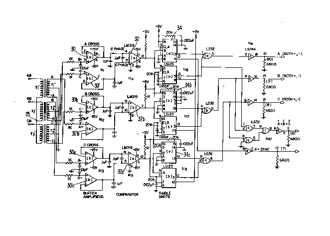
in the circuit schematic diagram of Fig. 6. In Fig. 6,
it is seen that the A phase, the B phase and the C phase
are input to the primary coils of T1, T2 and T3 and that
the common terminal 25 is shown for the primary coils for
these three transformers. The secondary coils Tl", T2 "
and T3 " are shown as they are connected to the balance
of the circuit in Fig. 6. In Fig. 6, there is shown that
a zero crossover leg for the A phase Which will serve as
the initial example of the circuit in Fig. 6. In the leg
for the A phase, the transformer T2 has its secondary coil
T2 " connected with the -b voltage connected to the
positive input of a first huffer amplifier 30 and the
center tap connected to a ground potential. The
tranaformer T3 has its secondary T3'' with the poi~itive c
MA9-88-027 7
" ' ~ ' :
2004340
terminal connected to the positive terminal of a ~econd
buffer amplifier 30' and its center tap connected to
ground potential. The output of the ~irst comparator 30
is applied to the positive input of the comparator 32 and
the output of the buffer amplifier 30' is connected to the
negative input of the comparator 32. The function of the
comparator 32 is to determine when the output of the
buffer amplifier 30 is equal in magnitude and opposite in
polarity from the output of the buffer amplifier 30'. At
the instant when that relationship occurs, the comparator
32 outputs a signal which indicates the zero crossover
event for the A phase. The particular operation of the
circuit of Fig. 6 i8 shown in Fig. 7, where it is seen that
the output of the comparator 32 is a transition from a
positive 5 volt level to a negative approximate 13 volt
level. That transition direction indicates that the A
phase i8 undergoing a positive to negative transition and
the time of occurrence of the transition is the time of
occurrence of the zero crossing for the A phase. If the
output of the comparator 32 is transitioned from -14 volts
to ~5 volts, this indicates that the A phase transition
i~ made from a negative to a positive value in the
occurrence of the zero crossover event. The output of the
comparator 32 is applied to the input as a single shot
circuit 34 which generates a small square wave pulse
indicating the instant of occurrence of the transition
.. . .
shown at the output of the comparator 32. The output of ~ -
.,
the single shot 34 can be used as a binary value signal
MA9-88-027 8
:-'';. '~
. ' '.' . :.
,': , - .
:
200~340
which can be applied to utilization circuits such a~ the ;~
waveform coincidence detector circuit of the Ross and
Woodworth patent, described above and as is seen in Fig.
8 herein.
As can be seen in the circuit diagram of Fig. 6, each -
respective zero crossover phase is identified by means of
a particular monitoring leg, the A phase leg having been
described above.
The B phase leg consists of a buffer amplifier 30b
and 30b' whose outputs are applied to the input of a
character 32b. The output of the comparator 32b is then
applied to a single shot 34b which provides a binary
signal output which can be applied to utilization logic.
The C phase monitoring leg includes the buffer
amplifier 30c and 30c'. The outputs of the buffer -
amplifier 30c and 30c' are applied to the inputs of the
comparator 32c. The output of the comparator 32c can be
applied to a single shot 34c. The output of the single
shot 34c will be a binary value which can be applied in ;;;
logic utilization circuits.
It can be seen that in the B phase monitoring leg,
the comparator 30b has it# positive input terminal
connected to the ~econdary T3" and to its negative c
terminal and that the buffer amplifier 30b and the buffer
amplifier 30b' has its positive input terminal connected
to the +a terminal of the secondary T1" .
In the C phase monitoring leg, it can be seen that
the buffer amplifier 30c has its positive input terminal
. ~:', '','': '
MA9-88-027 9 ;~
~' ' ' '
: ' '~ ' -
~'` .
`--` 200~a340
connected to the negative a terminal of the Tl'' sçcondary
and that the buffer amplifier 30c' has its positive
terminal connected to the +b terminal of the T2''
secondary.
The operation of the invention provides a noise
tolerant zero voltage crossover detector for all three
phases of a three phase power system. -
Although a specific embodiment of the invention has
been disclosed, it will be understood by those having
skill in the art that minor changes can be made to the
details of this specific embodiment without departing from
the spirit and the scope of the invention. ~: -
-' ~, '
.. .
~;."`;.~
' ~
MA9-88-027 10
" ' '''-' . '
:",. ''
,:
"'','~