Note: Descriptions are shown in the official language in which they were submitted.
- 1 - 2004555
1 TITLE OF THE INVENTION
Superconductive ~lectromagnetic Wave Mixer and
Superconductive Electromagnetic Wave Mixing Apparatus
~mploying the Same
~ O~ND OF THE INVENTION
Field of the invention
The present invention relates to a heterodyne
mixer that employs a superc~n~l~ctor, utilized in
10 detecting electro~agnetic waves such as millimeter
waves, and an electromagnetic wave mixing apparatus
that employs such a mixer.
Related Background Art
Het~dyl~e detectors utilized in detecting
15 electromagnetic waves such as millimeter waves have
been hitherto constituted of an antenna, a local
oscillator such as a Gunn oscillator or a klystron
and a heterodyne mixer device.
As the heterodyne mixer devices,
20 heterodyne mixer devices employing Josephson junctions
comprising a metal such as Nb are used, which mixer
devices have been so constituted as to have an SIS-
type laminated structure so that its junctions can have
capacitance.
In the conventional heterodyne detectors,
however, the local oscillator and the Josephson mixer
,- 7p
- 2 - 2004555
device are ~eparate7y constituted from each other, and
the e are connected with each other using a waveguide,
resulting in a very large-scale apparatus. In
addition, the local oscillator is re~uired to have an
output of from lO nW to 100 nW, also bringing about a
great power diqsipation.
To cope with these problems, an integral-type
heterodyne mixer has been devised in which a niobium
plane-type wea~-link Josephson junction is used at the
local oscillator and mixer ~ection("Josephqon Triode , in
D~NSHI TS~SHIN GAKKAI RON~UNS~I (Journal of Electron
Transmission Society) '86/5, Vol. J69-C, p.639; DENSI
JO~HO TSUSHIN GAKKAI-SHI, '87/5 SCE 87-9, p.49). This
Josephson triode is of integral type, and hence can make
the apparatus greatly compact.
BRIEF DESCRIPTION OF THE DRAWINGS
Figs. lA to lD, schematically illustrate a
~o~cas for ~ ring a -u~ .,ductive
el~ magnetic ~ave mixer according to an embodiment
of the present invention;
Fig. lE schematically illustrates another
embodiment of the present invention;
Figs. 2A to 2E show another ~o~c~s
corresponding to Ftgs. lA to lD;
Figs. 3A and 3B schematically illu~trate
another embodi~ent of the ~.~ent invention;
~ 3 - 2G04555
Figs. 4A to 4D schematically illustrate
an ~ erp.ocess for preparing a -u~e~o~ ctive
electronagnetic wave mixer according to another
e~bodiment of the pre~ent inventioni
Fig. 5 schematically illustrate~ another
embodiment of the ~.-c -nt invention;
Figs. 6A to 6C schematically illustrate a
superconductive ele L.~magnetic-WaVe mixer according
to still another embodi~ent of the prescnt
invention;
Figs. 7A to ~E schematically illustrate a
superconductive electromagnetic wave mixer according to
an e~boAiment of the ~e_c.,t invention;
Fig. 8 ~che~atically illustrates an e~uivalent
circuit of the device shown in Fig. 7C;
Fig. 9 schematically illustrates a
o~ductive elLc~.~magnetic wave mixer according to
an embodiment of the ~ ~nt invention;
Figs. lOA to lOD schematically illustrate a
8~ o~ ctive electromagnetic ~ave mixer according to
an embodiment of the ~.___..t invention;
Figs. llA and llB schematically illustrate a
prior art Jo~ephson triode;
Fig. 12 schematically illustrates an
embodi~ent of a ~ixing apparatu~ employing the
~c.~ ctive electromagnetic wave mi~er of the
pre~ent invention; and
2004555
Fig. 13 schematically illustrates another
embodiment of the mixing apparatus e~ploying the
~e.c4..l~ctive electromagnetic wave mixer of the
~ t invention.
Fig. llA schematically illustrates a
constitution of the above Josephson triode, numeral 1
designates a ~.,ve~-Ler terminal, 2 designates an
ocsillator terminal, 3 designates a co~mon ground.
Fig. llB illustrates an equivalent circuit thereof.
Among three wea~-link Joseph on junctions JJ1, JJ2 and
JJ3, JJ1 is used as a converter for het~G~y
detection, JJ2, as an oscillator for local
oscillation, and JJ3, as an isolator for ~eparating
JJl from JJ2. The device is ~c,~ed by applying a
15 bias cu,~-et to JJ2 to cause local oscillation
attributable to the AC Josephson effect, and mixing
the 8ignals resulting from this local oscillation and
an externally originating eloc~.~magnetic wave in the
JJl serving as the c~ er so that an internediate
fre~uency ~ignal is obtained.
In the above Jo~eph~on triode, ~ cv~r, it is
nece~ary to set the characteristics of nor~al
anc Rnl3, Rn12, Rn23, etc. the several Josephson
junctions each at a proper value. In the conventional
Josephson junction of a weak-link type of junction
employing a material such as Nb, however, it is
difficult to control the characteristics at the time
- 5 - 2004555
of manufacture. Hence, the above Josephson triode can
be manufactured wlth great difficulty.
Moreover, the above conventional apparatus or
device employs the material such as Nb, having a ~ow
critical temperature Tc (around the li~uid helium
temperature), 50 that the device must be made to
operate at a low temperature, re~uiring a very large-
scale cooling apparatus in which the Joule-Thomson
effect is utilized. In addition, the maximum
fre~uency that has beenused is as low as about 1 T~z,
and hence the recent demand of providing a high-
frequency band mixer can not be completely satisfied.
SUMMARY OF THE INVENTION
On ~ nt of the problems involved in the
above prior art, an ob~ect of the ~ ..t invention is
to ~ake it possible to realize an integral-type
elc_L~magnetic wave mixer capable of being prepared
with a good .~ cibility, having a very simple
structure, and employing an oxide ~ . o~ ctor.
The ~-~ -nt invention provides a
~ G~ ctive el~i~L~omagnetic~wave mixer comprising
a local-oscillator source and a receiving section,
said recelving section serving as a section at which
an electromagnetic wave from the local-oscillator
source and an externally originating electromagnetic
wave are combined; ~.}.~-cin said local-oscillator
source and said receiving ~ection are forned by at
- 6 - 2004555
}east one Josephson junction employing at ieast one
oxide superconductor, respectively.
In another embodiment, the pre~ent invention
provides a ~uperconductive electromagnetic wave mixer
co~prislng a loca}-oscillator source and a receiving
~ection, said receiving ~ection ~erving as a ~ection
at which an electromagnetic wave from the locat-
oscillator source and an externally originating
e}e_L~omagnetic wave are combined, wherein said local-
oscillator source and said recei~ing section arefor~ed by at least one Jo~ephson junction employing at
least one oxide supcrconductor, respectively, and said
local-oscillator source and ~aid receiving ~ection
~re coupled through a ~n~rtive uaterial.
The present invention also provide~ a
~u~c~conA-lctive electro~agnetic-wave mixing apparatus
comprising:
a ~u~c~o~ductive electro~agnetic wave mixer
co~prising a local-oscillator source, and a receiYing
s~ction at which an electromagnetic wave fro~ ~aid
loca}-oscillator source. and an externally originating
electromagnetic wave are combined, said loca}-
osc$11ator source and Qaid receiving section being
for~ed by at least one Josephson junction employing at
least one oxide superconductor, respectively;
.,
2004555
7 --
an i..L.~d~cing means through which the
externally originating electromagnetic wave is
introduced into the recei~ing ~ection of said
el~ agnetic wave mixer;
an amplifier that amplifies the
elc_ ~L omagnetic wave of an intermediate ~requency
band obtained as a result of the mixing in ~aid
ele~o~agnetic wave mixer; and
a cooler that coo}s at least said
el_~t~o~agnetic wave mixer.
DET~Tr~n ~ rpTIoN OF TH~ r~r~K~v ~MBOD~NB~TS
The ~u~c.~ rtive electromagnetic wave ~ixer
of the ~ nt invention will be described below u~ing
schematic ~llustration~ of its structure.
In the first embodiment of the --~c.c~ Yctive
electromagnetic-wave ~i~er of the ~ nt invention, a
plura7lty of Josephson junction regions comprised of
cry~tal grain ~o~nA-~ie~ of an oxide ~ v~A~tor
thin film are coupled interposing an insulating layer
~ .L_n them. In its operation, a bia~ vol~age is
applied to a Josephson junction region used as the
- 8 - 2004555
1 local-oscillator section(source)among the above plurality of
Josephson junction regions so that a local oscillator
signal is generated. This local-oscillator signal and
the externally originating electromagnetic wave are
5 combined (or undergo mixing) at the Josephson junction
region used as the receiving section among the above
plurality of Jo ephson junction regions, and the
intermediate frequency signal is thus taken out.
Description will be specifically made with
10 reference to the drawings. The first embodiment of
the superconductive electromagnetic wave mixer of the
present invention is roughly grouped into a plane type
as shown in Figs. lC and lD, a la~inate type as shown
in Figs. 2D and 2E, and also a multiple type a shown
15 in Figs. 3A and 3B.
Firstly, Figs. lC (a plan view) and lD (a
cross ~ection along the line a-a' in F~g. lC)
illustrate a plane-type superconductive
electromagnetic wave mixer, in which on the substrate
20 4 two Josephson junction regions 6 and 7 comprised of
crystal grain boundaries of the oxide superconductor
thin film 5, which regions ~erve as the local-
oscillator section and the receiving section,
respectively, and in which these local-oscillator
25 section and receiving ~ection are laterally arranged
interposing the in~ulating material 8 between them.
20045SS
g _
1 This plane type superconductive
electromagnetic wave mixer can be prepared by a method
comprising depositing one layer of the oxide
superconductor thin film 5 of a polycrystalline on the
5 substrate 4, followed by patterning using a technique
such as photolithography or ion implantation, and then
bringing the two Josephson junction regions 6 and 7
into a very close plane arrangement interposing the
insulating material 8 between them.
Secondly, Figs. 2D (a plan view) and 2E (a
cross section along the line b-b' in Fig. 2D)
illustrate a laminate type superconductive
electromagnetic wave mixer, in which on the substrate
4 two Josephson junction regions 6 and 7 comprised of
15 crystal grain boundaries of the lower and upper
films 5a and 5b, are laminated interposing the
insulating material 8 between them, and the regions 6
and 7 serve as the local-oscillator section and the
receiving section, respectively.
This laminate type superconductive
electromagnetic wave mixer can be prepared by a method
comprising depositing on the substrate 4 the lower
film 5a, the insulating material 8 and the upper film
5b in this order, followed by patterning using a
25 technique such as photolithography, thus, the two
Josephson junction regions 6 and 7 can be arranged
- lO- 2004555
1 close each other interposing the insulating material 8
between them.
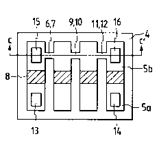
Thirdly, Figs. 3A (a plan view) and 3B (a
cro~ section along the line c-c' in Fig. 3A)
5 illustrate a multiple type ~uperconductive
electromagnetic wave mixer, in which on the substrate
4 the lower and upper films Sa and 5b are laminated
~nterposing the insulating material 8 between them,
and the JoQephson junction regions 6, 9 and 11 serving
10 as local-oscillator sections and Josephson junction
regions ~, 10 and 12 serving as receiving sections are
formed interposing the insulating material 8, and
further the electrodes 13, 14 and 15, 16 are formed.
The multiple type mixer specifically refers to
15 a superconductive electromagnetic wave mixer of the
type in which the respective local-oscillator sections
and receiving Qections are contained in a plural
number. This multiple type superconductive
electromagnetic wave mixer can be prepared by the same
20 method as the method of preparing the above laminate
-type superconductive electromagnetic wave mixer,
except that a larger number of Jo~eph~on junctions are
formed by patterning.
Though not shown in the drawings, it is also
2~ possible in the plane type superconductive
electromagnetic wave mixer previously described to
20~55
1 respectively form the local-oscillator section and
receiving section into multiplicity. Needless to say,
such a plane type multiple superconductive
electromagnetic wave mixer is also embraced in the
5 first embodiment of the present invention.
In the above embodiment, the Josephson
junction region comprised of crystal grain boundaries
of an oxide superconductor thin film is used. Any
preparation method, material and form may be employed
10 so long as the polycrystalline thin film of an oxide
superconductor is used. The insulating material
through which the two Josephson junction regions are
coupled together may be made of any materials, by any
method and in any form, including insulating thin
15 films comprising MgO, YSZ ~yttrium stabilized
zirconia) or a polymer of an organic substance, those
obtained by making an oxide superconductor into an
insulating material by means of ion implantation or
the like, or gaps or level differences formed by means
20 of etching or the like, where substantially the same
effect can be obtained.
In a second embodiment of the superconductive
electromagnetic wave mixer of the present invention, a
plurality of Josephson junction regions comprised of
25 crystal grain boundaries of an oxide superconductor
thin film are coupled through a conductive material
555
- 12 -
1 between them. Its operation is same as in the above
first embodiment.
Description will be specifically madè with
reference to the drawings. The second embodiment of
5 the superconductive electromagnetic wave mixer of the
present invention is roughly grouped into a plane type
as shown in Figs. 4C and 4D, and a multiple type as
shown in Fig. 5.
Firstly, Figs. 4C and 4D (4D: a plan view of
10 Fig. 4C) illustrate a plane type superconductive
electromagnetic wave mixer, in which on the substrate
4 two Josephson junction regions 6 and 7 of a plane-
type or quasi-plane-type comprised of crystal grain
boundaries of the oxide superconductor thin film 5,
15 one region of which serves as the local-oscillator
section and also the other region of which serves as
the receiving section, are provided, and the above two
Josephson junction regions 6 and 7 are coupled using
the conductive material 17.
The superconductive electromagnetic wave mixer
according to the present embodiment can be prepared,
for example, in the following manner: First, on the
substrate 4 made of MgO or the like, the
superconductive thin film 5 is formed (Fig. 4A).
25 Next, patterning is carried out by photolithography or
the like to form two Josephson junction regions 6 and
;~OC)~;5
- 13 -
1 7 (Fig. 4B). Then, the conductive material 17 taking
the form of extending over the two Josephson junction
regions is formed (Fig. 4C).
Secondly, Fig. 5 illustrates a multiple type super-
5 conductive electromagnetic wave mixer, in which on the
substrate 4 the oxide superconductor thin film 5, which is
subjected to patterning to form Josephson junction
regions 6a, 6b and 6c serving as local-oscillator
sections and Josephson junction regions 7a, 7b and 7c
10 serving as receiving sections, are provided and the
local-oscillator sections and the receiving sections
being coupled through the conductive material 17, and
electrodes 13, 14 and 15, 16 being further formed.
This multiple type superconductive electromagnetic
15 wave mixer can be prepared by the same method as the
method of preparing the above plane type (or quasi-
plane type) superconductive electromagnetic wave
mixer, except that a larger number of Josephson
junctions are formed by patterning.
In the above embodiment, the Josephson
junction region comprised of crystal grain boundaries
of an oxide superconductor thin film is used. Any
preparation method, material and form may be employed
so long as the polycrystalline thin film of an oxide
25 superconductor is used.
The conductive material through which the
s~s
- 14 -
1 local-oscillator sections and receiving sections are
coupled together may be made by any method and of any
materials so long as it is a conductive material such
as a metal, a semiconductor, or a superconductor.
In the third embodiment of the superconductive
electromagnetic wave mixer of the present invention,
it comprises a local-oscillator section and a
receiving section constituted of a tunneling Josephson
junction using an oxide superconductor thin film,
10 respectively, and said local-oscillator section and
receiving section being coupled by any of Josephson
junction, capacitance, resistance and inductance
formed of a conductive material or insulating
material.
Figs. 6A to 6C schematically illustrate an
example of the structure of the superconductive
electromagnetic wave mixer according to the present
embodiment, and a preparation method therefor.
First, on the substrate 4 made of, for
20 example, MgO, the lower film 5a is formed, the
insulating material layer 8' is formed thereon, and
the upper film 5b is further formed thereon (Fig. 6A).
Next, patterning is carried out by photolithography or
the like to form the groove 18 (Fig. 6B). Here,
25 superconductive properties change at the bottom
(coupling part 19) of the groove as a result of
2(~ iS5
- 15 -
1 processing as exemplified by ion milling, and the
desired characteristics of any of the insulating
material and the conductive material can be obtained.
The conductive material herein mentioned includes even
5 semiconductors and superconductors. This utilizes the
property that the characteristics of oxide
superconductors are very sensitively governed by
compositional ratios. A pair of tunneling Josephson
junction regions having Josephson current values
10 suited to the local-oscillator section and receiving
section can also be formed by changing right and left
extent of the groove 18. Here, the groove 18 need not
be physically cut so long as the groove is capable of
changing the degree of the coupling of the right and
15 left Josephson junction regions, and may be formed by
ion implantation or the like as shown in Fig. 6C. In
the device as shown in Figs. 6A to 6C, a bias current
is applied to the left-side Josephson junction region
20 to generate a local-oscillator signal, and the
20 signal is introduced into the right-side Josephson
junction region 21, where the mixing with the
electromagnetic wave irradiated from the outside is
carried out to achieve heterodyne detection. In Figs.
6A to 6C an example is shown in which the device is
25 processed after lamination, but the preparation method
is not limited to this.
2~04555
- 16 -
1 In the respective embodiments, in order for
the device to operate as an electromagnetic wave
mixer, the relationship I1 > I2 > I3 is required to be
established between the value I1 for the Josephson
5 current flowing through the Josephson junction region
that forms the local-oscillator section, the value I2
for the Josephson current flowing through the
Josephson junction region that forms the receiving
section, and the value I3 for the isolator current
10 that may flow between the above local-oscillator
section and receiving section.
For the achievement of the unbalance between
these current values, it is possible to use, in the
first embodiment, a method in which, for example, the
15 widths of the Josephson junction regions 6 and 7 as
shown in Fig. lC are made different (the width of the
local-oscillator section > the width of the receiving
section~, or the film 26 such as an MgO thin film, a
Zr2 thin film or an Ag thin film is deposited only
20 beneath the receiving section so that the
superconductivity may be changed at its upper part
(see Fig. lE~. This method is preferred because the
respective Josephson current values can be readily
controlled only by variously selecting the materials
25 or changing conditions for film formation. A similar
method is possible also in the second embodiment. In
X0045S5
- 17 -
1 the third embodiment, it is possible to use a method
in which, for example, the Josephson junction regions
20 and 21 as shown in Figs. 6B and 6C are coupled to
give a junction unbalanced in its extent.
Materials that can be used for the above film
26 include, for example, the following:
Ag, Au, Nb, NbN, Pb, Pb-Bi,
MgO, ZrO2, SiOx, a-Si, and other oxides.
In the case that Josephson current may be
10 increased by the above methods for controlling
Josephson current, the Josephson junction serves as
the local oscillation section, while in the case that
Josephson current may be decreased by the above
methods, the Josephson junction serves as the
15 receiving section.
The superconductor that constitutes the oxide
superconductor thin film in the respective embodiments
described above, when represented by the formula A-B-C-
D, it is desirable that A is at least one element
20 selected from the group consisting of La, Ce, Pr, Nd,
Pm, Sm, Eu, Gd, Tb, Dy, Ho, Er, Tm, Yb, Lu, Sc, Y, and
Bi; B is at least one element selected from the group
consisting of Ca, Sr, Ba, and Pb; C is at least one
element selected from the group consisting of V, Ti,
25 Cr, Mn, Fe, Ni, Co, Ag, Cd, Cu, Zn, Hg, and Ru; and D
is 0.
20~)4555
1 More specifically, it includes;
~1) 214 type:
(La1_xMx)2cu04_~ (M = Na, Ca, Sr, Ba)
(Ln, Sr, Ce)2CuO4 ~ (Ln = a lanthanoid such as
Nd)
(Ln, Ce)2CuO4 ~ (Ln = a lanthanoid such as Pr
or Nd)
(2) 123 type:
Ln(Ba2Cu307 ~ (Ln = any sort of lanthanoids),
and those wherein Ln has been substituted with
any sort of elements)
~3) Bi base:
Bi Sr CuO ~ Bi25r2_xLnxCuOy, Bi2 2 2 y
2 3-xLnxcu2oy~ Bi2-xpbxsr2ca2cu3o
Bi2Sr(LnCe)2Cu20y.
(In the above, Ln = any sort of lanthanoids),
(4) Tl base:
Tl2Ba2CanCu1+nOy ~n = O, 1, 2, 3 .... .),
TlBa2CanCu1+nOy (n = O, 1, 2, 3 ..... ).
20 (5) Pb base:
Pb2Sr2Ca1_xLnxCu30y (x = about 0.5)
(6) 223 type:
(LnBa)2(LnCe)2Cu30y (Ln: a lanthanoid).
Use of materials having a critical temperature
25 of not less than 77 K as exemplified by Y-Ba-Cu-O-
based, Bi-Sr-Ca-Cu-O-based or Tl-Ba-Ca-Cu-O-based
2004555
- 19 -
1 superconductors may also make it possible to use
inexpen~ive liquid nitrogen a~ a refrigerant. When
the mixer is continuou~ly driven, it i~ possible to
use a compact and inexpen~ive cryo tat having no Joule-
5 Thomson valve, thus bringing about an effective
Josephson triode as the mixer of an integral type.
When the materials of the above types are used, the
energy gap 2~ is several 10 meV, which is larger by
one figure than that of niobium. This means that the
10 maximum frequency that can be used in a mixer extendQ
up to about 10 THz, which is higher by oneorder of magnitude
than that of niobium (about 1 THz).
The superconductive materials constituting
the local-oscillator section and the receiving section
15 may be composed of plural materials, respectively.
A mixing apparatuq employing the
superconductive electromagnetic-wave mixer
described above will be described below.
The superconductive electromagnetic wave
20 mixing apparatus of the present invention comprises:
a ~uperconductive electromagnetic wave mixer
comprising a local-oscillator -ection, and a receiving
section at which an electromagnetic wave from said
local-oscillator section and an externally originating
25 electromagnetic wave are combined, said local-
oscillator section and said receiving section being
~rr
2004S55
- 20 -
1 formed by at least one Josephson junction employing at
least one oxide superconductor, respectively;
an introducing means through which the
externally originating electromagnetic wave is
5 introduced into the receiving section of said
electromagnetic wave mixer;
an amplifier that amplifies the
electromagnetic wave of an intermediate frequency
band, obtained as a result of the mixing in said
10 electromagnetic wave mixer; and
a cooler that cools at least said
electromagnetic wave mixer.
The apparatus will be detailed below with
reference to the drawings. First, as Fig. 12 shows,
15 the above superconductive electromagnetic wave mixer,
designated as 30, is installed in the cooler 31, such
as cryostat and the externally originating
electromagnetic wave 32 is introduced into the
superconductive electromagnetic wave mixer 30 through
20 the introducing means 33 for the externally
originating electromagnetic wave 32, comprising a
waveguide, a horn type antenna, etc. A bias current
is also fed from the direct-current electric source 34
outside the cooler to the local-oscillator section of
25 the superconductive electromagnetic wave mixer 30 to
cause oscillation with a desired frequency. The
- 21 - 2004555
1 externally originating electromagnetic wave 32 and the
local-oscillator wave are combined tor caused to
undergo mixing) to give the electromagnetic wave 35 of
an intermediate frequency band (IF). This IF wave 35
5 is amplified using an amplifier 36, so that the output
37 after heterodyne mixing can be obtained.
In Fig. 12, the introducing means 33 and the
amplifier 36 are provided in~ide the cooler 31, but,
without limitation thereto, at least the
~pe-~nductive electromagnetic wave mixer 30 may be
cooled in the cooler 31.
In the superconductive electromagnetic wave
mixing apparatus of the present invention, a preferred
embodiment is the embodiment as ~hown in Fig. 13, in
15 which the waveguide 38 is used as the introducing
means and the superconductive electromagnetic wave
mixer 30 is provided inside such the waveguide 38.
~hi~ embodiment, in which the superconductive
electromagnetic wave mixer having even the local-
20 oscillator section inside the waveguide is provided,enables generation of local-oscillator waves within
the ~ame clo~ed space as that for the introducing
means for the externally originating electromagnetic
wave; so that the mixing efficiency increa~es, in
25 other words, the efficiency of the propagation of
electromagnetic waves to the receiving section
..~
,., ~
... .
- 22 - 2004555
l increases. It is also more preferable that the power
of local-oscillator outputs can be decreased, which i5
accompanied with a decrease in the inflow of heat due
to the Joule heat, ~o that not only the device itself
can be made compact with it~ advantages well
exhibited, but also the whole apparatus including the
cooler can be made to operate with a low power
di~sipation and made compact.
The superconductive electromagnetic wave mixer
10 of the present invention is equipped with both the
local-oscillator section and the heterodyne mixer
section in the sa~e device, compared with the prior
art hete~ody~-c detectors as previously discussed.
Thus, it became unneces~ary to provide an external
15 local oscillator and a waveguide for making
connection thereto, and also it became possible to
make the mixing apparatus very compact. In addition,
the use of the external local oscillator has always
required a local-oscillator output of from 10 nW to
20 100 nW, but the device according to the present
invention requires that of only from 0.1 nW to 1 nW,
having made it po~sible to greatly decrease the power
dissipation.
According to the present invention, it is
25 further possible to prepare an electromagnetic wave
mixer that can operate at a relatively high
~,'
)4~
1 temperature (around the liquid nitrogen temperature),
using the oxide superconductor having a relatively
high critical temperature Tc. Thus, it has become
- possible to construct a compact and inexpensive system
5 with a simplified cooling unit.
Moreover, the mixer of the present invention
has made it possible to be used as a device for high
frequency bands, probably because it employs the oxide
superconductor having a larger band gap than that of
10 Nb or the like ~the energy gap of Nb is about 3 meV,
but that of the oxide superconductor as exemplified by
a Y-based superconductor is larger than it by one
figure). More specifically, a possible frequency
limit was found to be about 700 GHz in the case of Nb,
15 and about 10 THz in the case of Y-based
superconductors. This further means that the
information transmission speed is 10 times and the
band width is also 10 times, namely, the information
that can be transmitted in the same time increases by
20 nearly two figures.
It has also become possible to successfully
couple the local-oscillator section and the receiving
section by virtue of the oxide superconductor having
the property that the electrical characteristics may
25 greatly change depending on the compositional changes.
It has further become easy to obtain the desired
- 24 - 20Q4555
1 Josephson current values because of the junction made
to comprise the tunneling Josephson junction. The
foregoing has made it possible to prepare a Josephson
triode in a good yield.
It is more preferable to couple the local-
oscillator section and receiving section of the mixer
through an insulating material or a conductive
material, than to form a gap between them. More
specifically, it was found that, also when they were
10 coupled through an insulating material, the dielectric
constant of the insulating material was larger than ~0
of vacuum by about one order of magnitude, the electric
capacity held between the local-oscillator section and
receiving section was also larger than the case when
15 the gap was formed between them, and thus the couple
between the two sections was considered to have become
stronger, bringing about, however, an increase in the
mixing efficiency (i.e., the efficiency of the
propagation of electromagnetic waves from the local-
20 oscillator section). This further resulted in a stillstronger couple when an insulating material was
replaced with a conductive material, and hence a
greater improvement was seen in the mixing efficiency.
A Josephson junction of a grain boundary type
25 is of weak-link type, which is more preferable than a
tunneling Josephson junction with respect to the
,, ,
. . ,
20~)45~;5
- 25 -
1 maximum frequency used and a mixing efficiency. This
is also preferable in the sense of well making the
most of the advantage resulting from the employment of
the high-temperature oxide superconductor that can be
5 applied to high-frequency bands, as previously
mentioned.
The Josephson junction region that constitutes
the local-oscillator section may be made plural in
number, whereby the voltage to be applied to the local-
10 oscillator section can be made larger and thus thelocal-oscillator frequency can be made stabler.
The Josephson junction region that constitutes
the receiving section may also be made plural in
number, whereby the detection efficiency can be
15 improved.
EXAMPLES
The present invention will be described below
in greater detail by giving Examples.
Example 1
Figs. 2A to 2D schematically illustrate the
structure of, and preparation steps for, a
superconductive electromagnetic wave mixer according
to an embodiment of the present invention.
In the steps as shown in Figs. 2A to 2B, the
lower film 5a of YlBa2cu3o7-x (x o t
Z004555
- 26 -
1 0.5) was formed on the substrate 4 by the cluster ion
beam method (Fig. 2A). An SrTiO3 monocrystalline
substrate was used as the substrate 4. This film
formation was carried out under conditions as follows:
5 Y, BaO and Cu were used as evaporation sources, the
acceleration voltage and ionization current therefor
were 1 kV and 300 mA, respectively, for each element,
the substrate temperature was set to 500C, and oxygen
gas was introduced at 1 x 10 3 Torr at the time of
10 deposition. The lower film 5a was comprised of a
polycrystalline film with a film thickness of 0.1 ~m,
having crystal grains with a size of about 1 ~m, and
its resistance turned zero at a temperature of not
more than 83 K.
Next, an MgO thin film was formed by
deposition by RF sputtering method to form the
insulating material 8 (Fig. 2B). This film formation
was made under conditions as follows: Using an MgO
target, in a sputtering gas of Ar:02 = 1:1 under 1 x
20 10 2 Torr, the substrate temperature was set to 200C,
and the sputtering power, to 200 W. The resulting
layer had a film thickness of 0.08 ~m.
Subsequently, the upper film 5b was formed in
the same manner as the lower film 5a (Fig. 2C). This upper
25 film 5b showed zero resistance at a temperature of not
more than 81 K.
20~)~555
- 27 -
1 Patterning was further carried out by
photolithography to form two Josephson junction
regions 6 and 7 in a laminate form (Figs. 2D and 2E~.
The two Josephson junction regions 6 and 7 were each 2
5 ~m in width and 3 ~m in length.
The superconductive electromagnetic wave mixer
thus prepared was cooled to 40 K by means of a simple
cooling unit, and then a bias current was applied to
the Josephson junction region 7 from a DC electric
10 source to make it to the local-oscillator section, and
an electromagnetic wave was irradiated on the
Josephson junction 6 serving as the receiving section.
As a result, the device satisfactorily operated as a
mixer of electromagnetic waves in a frequency region
15 of from 100 GHz to 1 THz.
In the present Example, devices obtained by
replacing Y in the superconductive thin film material
Y1Ba2Cu307_x ~x = O to 0.5) with a lanthanoid such as
Ho, Er, Yb, Eu or La also similarly operated.
Example 2
Figs. lA to lE illustrate preparation steps
for a superconductive electromagnetic wave mixer
according to an embodiment of the present invention.
In the superconductive electromagnetic wave mixer
25 shown in these Figs. lA to lD, ion implantation by FIB
was carried out to a superconductive thin film to make
20C)4555
- 28 -
1 an insulating material.
First, on the substrate 4, the superconductive
thin film 5 was formed (Fig. lA). An MgO
monocrystalline substrate was used as the substrate 4.
As the superconductive thin film 5 used, a film,
which was formed by RF magnetron sputtering, using a
Bi25r2Ca2Cu3010 target under conditions of an Ar
pressure of 1 x 10 Torr, an RF power of 200 W and a
substrate temperature of lOO~C, and heating at 860~C
10 in the atmosphere after the film formation, was used.
This superconductive thin film 5 was comprised of a
polycrystalline film with a film thickness of 0.2 ~m,
having crystal grains with a size of from 2 to 3 ~m,
and exhibited superconductivity at a temperature of
15 not more than 95 K.
Next, patterning was carried out by
photolithography to form the narrow 5' in the
superconductive thin film 5 (Fig. lB). This narrow 5'
was made to have a dimension of 5 ~m in length and 8
20 ~m in width.
Subsequently, along the center line of this
narrow 5' Ar ions were further implanted by FIB in a
width of 0.5 ~m to form the insulating material 8.
Thus, the narrow 5' was divided into two parts to form
25 the Josephson junction regions 6 and 7 in a very close
arrangement, and at the same time the superconductive
2~0~5S
1 thin film 5 was divided into two parts (Fig. lC).
The superconductive electromagnetic wave mixer
thus prepared operated like that in Example 1.
In the present Example, devices obtained by
5 changing the superconductive thin film material to
Bi2_xPbxSr2Ca2Cu3010 or replacing Bi thereof with lead
also similarly operated.
Example 3
Fig. 5 schematically illustrates the structure
10 of a superconductive electromagnetic wave mixer
according to an embodiment of the present invention.
The superconductive electromagnetic wave mixer shown
in Fig. 5 was prepared according to the following
steps. First, using an MgO monocrystalline substrate
15 as the substrate 4, the oxide superconductor thin film
5 was formed thereon. The oxide superconductor thin
film 5 was formed by RF magnetron sputtering, using a
Bi2Sr2Ga2Cu3010 target under conditions of a
sputtering power of 150 W, a sputtering gas of Ar, gas
20 pressure of 2 x 10 3 Torr and a substrate temperature
of 100C to give a film thickness of 0.25 ~m, followed
by heating at 860C in an atmosphere of 30 % 2 and ~0
% N2. This thin film 5 turned to a polycrystalline
film having crystal grains with a size of about 2 ~m,
25 and exhibited superconductivity at a temperature of
not more than 95 K.
~004555
- 30 -
1 On this oxide superconductor thin film 5,
patterning was carried out by photolithography to form
Josephson junction regions 6a, 6b and 6c serving as
the local-oscillator sections and Josephson junction
5 regions 7a, 7b and 7c serving as the receiving
sections, all of which were made to be 4 ~m in both
width and length.
Next, Cr and Au were deposited by resistance
heating to give films of 0.01 ~m and 0.05 ~m,
10 respectively, in thickness, thus forming the
conductive material 17 and the electrodes
13, 14 and 15, 16.
The superconductive electromagnetic wave mixer
thus prepared was cooled to 40 K using a simple
15 cooling unit. As a result, it satisfactorily operated
as a mixer of electromagnetic waves in a frequency
region of from 100 GHz to 1 THz.
A voltage necessary for applying a bias current
to the local-oscillator section was larger than that
20 in Example 2 by three or four times, so a stable
operation could be achieved.
In the present Example, devices obtained by
changing the superconductive thin film material to
Tl2Ba2CanCu1+nOy (n = 1, 2 or 3) or TlBa2CanCu1+nO (n
25 = 1, 2 or 3) also similarly operated.
Example 4
~004~555
- 31 -
1 Figs. 3A and 3B schematically illustrate the
structure of a superconductive electromagnetic wave
mixer according to another embodiment of the present
invention. The superconductive electromagnetic-wave
5 mixer as shown in Figs.3A and 3B comprises the local-
oscillator section and receiving section which are
coupled interposing an insulating material so as to
form capacitance. Fig. 3A is a plan view thereof, and
Fig. 3B is a cross section along the line c-c' in Fig.
10 3A. This superconductive electromagnetic wave mixer
was prepared by the steps as follows: First, using an
SrTiO3 monocrystalline substrate as the substrate 4,
the lower film 5a was formed thereon. This lower film
5a was formed using the cluster ion beam method, and
15 using Y, BaO and Cu as deposition sources to deposit
them on the substrate so as to be Y:Ba:Cu = 1:2:1.5.
The acceleration voltage and ionization current
therefor were 1 kV and 300 mA, respectively, for each
element, and the deposition was carried out by
20 introducing oxygen gas of 1 x 10 3 Torr and setting
the substrate temperature to 500C. The lower film 5a
was comprised of a polycrystalline film with a film
thickness of 0.1 ~m, having crystal grains with a size
of about 1 ~m, and exhibited superconductivity at a
25 temperature of not more than 83 K.
Next, an MgO thin film was formed by
20~)4555
- 32 -
1 deposition by RF sputtering to form the insulating
material 8. This film formation was made under
conditions as follows: Using an MgO target, in a
sputtering gas of Ar:02 = 1:1 under 1 x 10 Torr, the
5 substrate temperature was set to 200C, and the
sputtering power, to 200 W. The resulting layer had a
film thickness of 0. oa ~m.
Subsequently, the upper film Sb was formed in
the same manner as the lower film 5a. This upper film
10 5b exhibited superconductivity at a temperature of not
more than 81 K.
These lower and upper films 5a and 5b were
further subjected to patterning by photolithography to
form Josephson junction regions 6, 9 and 11 serving as
15 the local-oscillator sections and Josephson junction
regions 7, 10 and 12 serving as the receiving sections
in a laminate form. Thereafter, Cr and Au were
deposited by resistance heating in a laminate form to
give films of 0.01 ~m and 0.05 ~m, respectively, in
20 thickness, thus forming the electrodes 13, 14 and 15,
16.
The superconductive electromagnetic wave mixer
thus prepared satisfactorily operated like that in
Example 3.
In the present Example, a device obtained by
changing the superconductive thin film material to
4555
- 33 -
1 Nd1 85CeO 15CuOy also similarly operated. This
material, however, had a Tc of about 25 K, and hence
was used by cooling it to 20 K. Also in the case that
the lower and upper films Sa and 5b were constituted
5 by different materials, the mixer operated similarly.
Example 5
In the steps as shown in Fig. 4, an MgO
monocrystalline substrate was used as the substrate 4,
and the superconductive thin film 5 of Bi2Sr2Ca2Cu30x
10 was formed on the substrate 4 by RF magnetron
sputtering. This film formation was carried out under
conditions as follows: In an atmosphere of Ar:02 = 1:1
and a pressure of 7 x 10 Torr, using a
Bi25r2Ca2Cu30x sinter as a target, the film was formed
15 at a sputtering power of 100 W and a substrate
temperature of 200C and the film thus formed was then
heated at 850C for 1 hour in an oxidizing atmosphere.
The film had a thickness of 0.8 ~m. This thin film
was comprised of a polycrystalline thin film having
20 crystal grains with a size of from 2 to 3 ~m (Fig.
4A). Next, patterning was carried out by
photolithography to form two Josephson junction
regions 6 and 7 in a close arrangement. The junction
regions each had a dimension of 8 ~m in length and 4
25 ~m in width, and the space between the two Josephson
junction regions was 1 ~m (Fig. 4B). Next, Ag was
2(~S55
- 34 -
1 vacuum-deposited thereon by resistance heating to form
a film of 0.5 ~m thick, followed by patterning by
photolithography to form the conductive material 1~
(Fig. 4C). Here, the Josephson junction is comprised
5 utilizing crystal grain boundaries (Fig. 4D).
The electromagnetic wave mixer thus prepared
satisfactorily operated as a heterodyne mixer of
electromagnetic waves in a frequency region of from
100 GHz to 1 THz.
In the present Example, a device obtained by
changing the superconductive thin film material to
Pb2Sr2CaO 5Yo 5Cu30y also similarly operated.
Example 6
Here will be described an instance in which,
15 in the embodiment shown in Fig. 4, SrTiO3 was used as
the substrate, a YBaCuO-based material was used as a
superconductive material, and cluster ion beam
deposition was used as a method of forming a
superconductive thin film. First, on the substrate 4,
20 the superconductive thin film 5 of Y1Ba2Cu307_x (x =
0.1 to 0.4) was formed by cluster ion beam deposition.
This film was formed under conditions as follows:
Using Y, BaO and Cu as evaporation sources, the
acceleration voltage and ionization current therefor
25 were 2 kV and 100 mA, respectively, for Y, 4 kV and
200 mA for BaO, and 4 kV and 200 mA for Cu. The
2()~0~555
- 35 -
1 substrate temperature was set to 600C, and 2 gas of
1.3 x 10 Torr was introduced at the time of
deposition. The resulting film had a thickness of 0.5
~m. This thin film was comprised of a polycrystalline
5 thin film having crystal grains with a size of about 2
~m, and exhibited superconductivity without heat
treatment ~Fig. 4A~. Patterning was carried out
thereon in the same manner as in Example 5 to form two
Josephson junction regions 6 and 7 (Fig. 4B). The
10 conductive material 17 was further formed in the same
manner (Fig. 4C).
The electromagnetic wave mixer thus prepared
satisfactorily operated like that in Example 5.
Example 7
Figs. lOA to lOD illustrate another
embodiment. This utilizes a level difference formed
on the substrate, for the formation of the Josephson
junction.
First, a level difference of 0.5 ~m was formed
20 by photolithography on the sbstrate 4 of an MgO
monocrystalline (Fig. lOA). Next, on the substrate 4
on which the level difference was made, the
superconductive thin film 5 of Er1Ba2Cu307 x (x = 0.1
to 0.4) was formed by RF magnetron sputtering. The
25 film was formed under conditions as follows: In an
atmosphere of an Ar gas pressure of 7 x 10 3 Torr,
20~4555
- 36 -
1 using a Er1Ba2Cu307_x (x = 0.1 to 0.4) sinter as a
target, the film was formed at a sputtering power of
lSO W and a substrate temperature set to 100C and the
film thus formed was then heated at gOOC for 1 hour
5 in an oxidizing atmosphere. The film had a thickness
of 0.5 ~m. This thin film was comprised of a
polycrystalline thin film having crystal grains with a
size of from 4 to 6 ~m (Fig. lOB). Next, patterning
was carried out in the same manner as in Example 5 to
10 form two Josephson junction regions 6 and 7. However,
the junction regions were each made to be 16 ~m in
length and 8 ~m in width (Fig. lOC). The conductive
material 17 was further formed in the same manner as
in Example 5 (Fig. lOD).
The electromagnetic wave mixer thus prepared
satisfactorily operated like that in Example 5.
Example 8
In the steps as shown in Fig. 6, an MgO
monocrystalline substrate was used as the substrate 4,
2 2 2 3 x
the substrate 4 by ion beam sputtering. This film
formation was carried out, using a Bi2Sr2Ca2Cu30
sinter as a target, under conditions of a background
pressure of 2 x 10 Torr, an Ar pressure of 3 x 10
25 Torr, an ion current of 100 ~A, an acceleration
voltage of 7kV, and a substrate temperature of 600CC.
~0~55
- 3~ -
1 The resulting film had a thickness of 0.05 ~m. Next,
the insulating material layer 8' of MgO was formed by
RF sputtering, using an MgO target, under conditions
of an Ar pressure of 7 x 10 Torr, a sputtering power
5 of 100 W, and a substrate temperature of 150C.
Further thereon, the upper film 5b of Bi2Sr2Ca2Cu3O
was formed under the above conditions (Fig. 6A).
Next, patterning was carried out by photolithography
to form Josephson junction regions 20 and 21 as shown
10 in Fig. 6B. Junction areas were 10 ~m x 8 ~m for the
Josephson junction region 20 and 5 ~m x 8~m for the
Josephson junction region 21. The groove 18 was 1 ~m
in width, and the film thickness at the coupling part
19 was 0.015 ~m.
At this time, current-voltage characteristics
between the lower film 5a of the Josephson junction
regions 20 and the lower film 5a of the the Josephson
junction 21 were measured at the liquid nitrogen
temperature to reveal that the characteristics of a
20 microbridge Josephson junction were exhibited. In
other words, the coupling part 1g was made up of a
weak-link Josephson junction. The Josephson current
was found to be 80 ~A.
The electromagnetic wave mixer thus prepared
25 was set in a waveguide under liquid nitrogen cooling
and evaluated. As a result, it satisfactorily
7~0~4~55
- 38 -
1 operated as a heterodyne mixer of electromagnetic
waves in a frequency region of from 100 GHz to 800
GHz.
Example g
Here will be described an instance in which,
in the steps shown in Fig. 6, SrTiO3 was used as the
substrate 4, a YBaCuO-based material was used as the
superconductive material, and the cluster ion beam
deposition method was used for forming the
10 superconductive thin film. First, on the substrate 4, the
lower film 5a of YBa2Cu307_x (x = 0.1 to 0.4) was formed
by cluster ion beam deposition. This film was formed
under conditions as follows: Using Y, BaO and Cu as
evaporation sources, the acceleration voltage and
15 ionization current therefor were 3 kV and 100 mA,
respectively, for Y, 5 kV and 200 mA for BaO, and 5 kV
and 200 mA for Cu. The substrate temperature was set
to 700C, and 2 gas of 5 x 10 3 Torr was introduced
at the time of deposition. The resulting thin film
20 was 0.06 ~m thick. Next, Ag was deposited with a
thickness of 0.002 ~um by resistance heating, and ZrO2
was formed thereon with a thickness of 0.001 ~m by RF
sputtering. At this time, YSZ was used as a target,
the Ar pressure was 7 x 10 3 Torr, the sputtering
25 power was 100 W, and the substrate temperature was
100C. The upper film 5b of YBaCuO of 0.08 ~m thick
2(~0~555
- 39 -
1 was further formed thereon by the above cluster ion
beam deposition at a substrate temperature set to
550C (Fig. 6A). Next, the Josephson junction regions
20 and 21 were formed by photollthography and cluster
5 ion implantation (Fig. 6C). The ion implantation was
carried out using Ar ions (5 keV). Junction areas
were 12 ~m x 10 ~m for the Josephson junction region
and 6 ~m x 10 ~m for the Josephson junction region
21. The part at which the ions were implanted was 0.8
10 ~m in width. The electric characteristics at the
coupling part 19 were measured in the same manner as
in Example 8, and were found to be semiconductive.
The resistivity at the liquid nitrogen temperature was
about 103 Q-cm.
The electromagnetic wave mixer thus prepared
satisfactorily operated at the liquid nitrogen
temperature, like that in Example 8.
Example 10
Figs. 7A to 7D illustrate an electromagnetic
20 wave mixer of Example 10. First, by the same process
as in Example 9, the lower film 5a composed of a Y-
based thin film of 0.06 ~m thick and Ag of 0.002 ~m
thick and the insulating material layer 8'composed of
Zr2 of 0.001 ~m thick in this order was formed on the
25 substrate 4, and patterning was carried out by
photolithography (Fig. 7A). Next, the upper film 5b
2(~04SSS
- 40 -
1 of Y-based thin film was formed thereon with a
thickness of 0.06 ~m, and patterning was carried out
by photolithography to form a series array of
tunneling Josephson junctions (Fig. 7B).
5 Subsequently, using an excimer laser, the left-end
junction was etched to form the groove 18 (Fig. 7C).
Figs. 7D and 7~ show cross sections along the lines a-
a' and b-b', respectively, in Fig. 7C. The groove 18
shown in Fig. 7C had a width of 0.5 ~m. The electric
10 characteristics at the coupling part 19 were measured
in the same manner as in ~xample 8 to reveal that the
resistivity was 106 Q-cm or more and the electric
capacitance was about 1 nF.
Fig. 8 shows an equivalent circuit of this
15 device.
Namely, both the local-oscillator section 23
and the receiving section 24 are set in 10 series
arrays. This constitution makes it possible to make
10 times larger the operation voltage applied when the
20 bias current is flowed to the local-oscillator
section, and also makes 10 times larger the voltage at
the receiving section. This can advantage the
stability and noise resistance required when the
device is actually operated.
The electromagnetic wave mixer thus prepared
satisfactorily operated as a heterodyne mixer of
555
1 electromagnetic waves in a region of from 100 GHz to
800 GHz at the liquid nitrogen temperature.
Example 11
The procedure of Example 2 was repeated to
5 form two Josephson junction regions, one of which was
made to have a width of 2 ~m, the other of which a
width of S ~m, respectively, and both of which a
length of 5 ~m in common. Here, the Josephson current
was 11 mA at the 2 ~m wide Josephson junction region,
10 which was used as the receiving section, and the
Josephson current was 23 mA at the 5 ~m wide Josephson
junction region, which was used as the local-
oscillator section.
As a result, the device satisfactorily
lS operated like that in Example 2, but it was possible
to take out the power of electromagnetic waves of
intermediate frequencies at a higher level than that
in Example 2.
Example 12
Fig. 9 schematically illustrates the structure
of a superconductive electromagnetic wave mixer
according to Example 12. The superconductive
electromagnetic wave mixer shown in Fig. 9 was
prepared according to the following steps.
2~ First, an MgO monocrystalline substrate was
used as the substrate 4. The thin film 26 of ZrO2 was
20045SS
- 42 -
1 formed only half on the substrate with a thickness of
only 0.002 ~m. The film was formed by RF magnetron
sputtering, using YSZ as a target, in a sputtering gas
of Ar:02 = 1:1 and a pressure of 1 x 10 2 Torr, at a
5 substrate temperature of 200C, and a power of 100 W.
Thereafter, the procedure of Example 3 was repeated to
form the local-oscillator section (7a, 7b and 7c) and
the receiving section (6a, 6b and 6c). Here, the
Josephson current at the local-oscillator section (7a,
10 7b and 7c) was 3.5 mA, and the Josephson current at
the receiving section (6a, 6b and 6c) was 0.7 mA. The
superconductive electromagnetic wave mixer thus
prepared satisfactorily operated like that in Example
3, but it was possible to take out the power of
15 electromagnetic waves of intermediate frequencies at a
higher level than that in Example 3.
Example 13
Fig. 13 illustrates the constitution of a
mixing apparatus according to Example 13.
A superconductive electromagnetic wave mixer
prepared by the method previously described in Example
1 was installed inside the rectangular waveguide 38 of
1 mm x 0.5 mm in inner size. This waveguide 38 was
fixed on the cold head 31' of the cryostat 31 using a
25 circulating helium gas and cooled to 15 K. Here, the
waveguide 38 is partitioned with the Teflon sheet 39
X0~)4555
- 43 -
1 of a 0.2 mm thick at the joining part thereof with the
cryostat 31, so that the inside of the cryostat is
kept vacuum. Under this constitution, using the
direct current electric source 34 provided outside the
5 cryostat, a bias current was fed to the local-
oscillator section of the superconductive
electromagnetic wave mixer described above. An
electromagnetic wave of 200 GHz was introduced into
the waveguide 38, using a gunn oscillator and a
10 frequency doubler, and the bias current was applied at
15 to 39 mA. As a result, it was possible to obtain
the mixing output 37 with an intermediate frequency of
1 to 0.7 GHz. Here, a GaAs FET amplifier was used as
the amplifier 36.