Note: Descriptions are shown in the official language in which they were submitted.
2~05194
72430-108
The present invention relates to a synchronizing circuit
for a demultiplexer for a digital time-division multiplex
communication system wherein a digital signal which is
asynchronous with the pulse frame and consists of successive
blocks whose beginnings are marked with sync words is inserted
into the pulse frame, said circuit deriving from a clock signal of
the received sync words a sync signal which exhibits less jitter
than the clock signal of the received sync words.
Such a demultiplexer is disclosed in DE-A1-34 39 633.
In the demultiplexer described there, the sync signal is derived
from the clock of the received sync words by correcting the word
clock with the aid of additional information transmitted to the
demultiplexer, such that the intervals between successive clock
pulses are equal to the intervals between the sync words of the
digital signal to be inserted into the pulse frame by the
multiplexer at the transmitting end, which are asynchronous with
the pulse frame. The jitter of the sync words caused by the
asynchronous insertion of this signal, also referred to as
"waiting-time jitter", is thus clearly reduced in the
demultiplexer.
This solution has the disadvantage that a circuit for
generating the additional information is required at the
transmitting end, and that through the transmission of this
additional information, the amount of useful information that can
be transmitted is reduced.
It is, therefore, the object of the invention to provide
a synchronizing circuit and demultiplexer which reduces the
B
2G05194
72430-108
waiting-time jitter without any steps having to be taken in the
associated multiplexer at the transmitting end.
This object is attained by a synchronizing circuit which
is characterized in that the circuit contains a measuring device
which measureæ the time intervals between the received sync words,
a filter which takes the average of the time intervals between
sync words, and a signal generator which forms the sync signal
from said average in such a manner that the pulse period of the
sync signal is equal to said average.
Further advantages of the invention are realized when
the filter takes the average of the different time intervals
between successive sync words successively over a predetermined
period of time, and rounds it to an integer N', the rounding error
being taken into account for the subsequent averaging by error
feedback. The filter can further include a counter in which an
assumed main distance between sync words is stored before the
circuit is put into operation, that the counter can increase or
decrease its count by a fixed amount only once during the interval
between two sync words, or leaves it unchanged, and that the
change is determined by the result of a numerical comparison
between the count of the counter and the sum of a subsequent count
appearing at the input of the filter and an error signal.
The invention will now be explained by way of example
with reference to the accompanying drawings, in which:
Fig. 1 is a block diagram of the novel circuit for
reducing waiting-time jitter;
.~
20051~
72430-108
Fig. 2 shows a first embodiment of the filter F of Fig.
1, and
Fig. 3 shows a second embodiment of the filter F of Fig.
1.
Referring to Fig. 1, when a sync word has been detected
in a sync-word detector (not shown), a pulse I generated in the
sync-word detector in response thereto is applied to a measuring
device M over two leads.
The measuring device M contains a counter 1 and a
register 2.
After receipt of a pulse I, the counter 1, clocked by a
2a
Z005~9~
word clock WT provided by the demultiplexer (not shown),
counts from zero until the next pulse I. It
has then reached a count N , which is a measure of the
time interval between these two pulses, i.e., between
the two successive sync words just received. Different
counts N; are possible, where i=O, 1, 2, ..., m, ...~ n, ... .
This count Nn is transferred into the register 2,
which is enabled by said next pulse I.
From the register 2, the count Nn is transferred into a
filter F, which is also controlled by the pulses.
The filter F takes the average N', rounded to an integer,
of the last received count and a predetermined number of
previously received counts.
This average N' is fed to a signal generator S consisting
of a down counter 3 and a comparator 4. After receipt
of the average N', the down counter 3, clocked at the
repetition rate of the word clock WT or an integral
multiple thereof, counts from the average N' down to
zero. Each numerical value is fed to the comparator 4,
which compares it with the numerical value zero. When
zero has been reached, the comparator produces a
sync signal SY, to be exact: the edge of a sync signal
SY, whosepulse period is equal to the average N'. The
sync signal SY serves as the input signal for a phase-
locked loop (PLL). It is fed back to the down counter
3, so that the latter can receive the next average N'
from the filter F.
, A . _
-`- 200S194
Fig. 2 shows a first embodiment of the filter F of
Fig. 1.
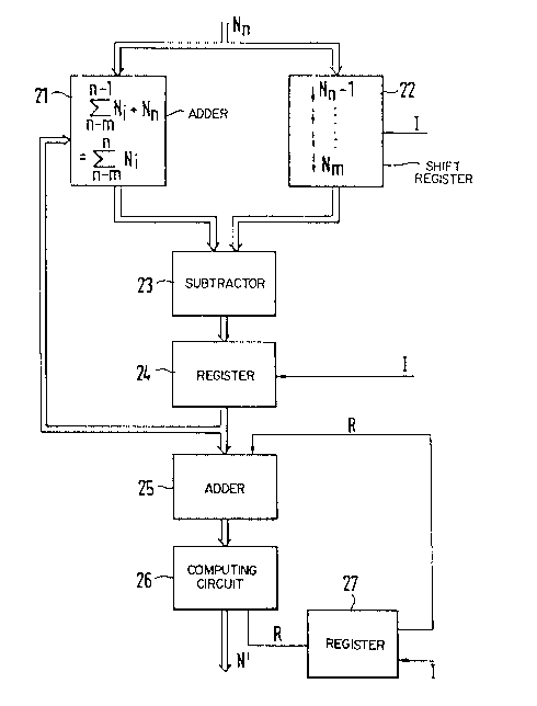
A count Nn ;s fed both to an adder 21, where it ;s
added to the sum of the last m counts up to N
received from the register 2, i.e.,
n-1 n
N; + Nn = ~ N;
i=n-m i=n-m
and to a shift reg;ster 22 containing the last m counts
N to N
n-m n-1
Each time a pulse I is applied to the shift register
22, the counts N; are shifted by one cell, the new
count Nn is inserted into the cleared cell of the
count Nn 1~ and the "oldest" count Nn m is applied to
a subtracter 23.
The latter has two inputs, which are connected to
theoutput of the shift register 22 and to the output
of the adder 21, respectively. It forms the difference
between the sum
n-1
N; + Nn = ~ N;
i=n-m i=n-m
zoo~9~
rom the output of the adder 21 and the count N
n-m
fromthe shift register 22:
n
> N; Nr~_~ ? N
1=n-m 1=n-m+1
The difference formed by the subtracter 23 is coupLed into a
register 24, which is also clocked by the pulses I.
From this register, it is transferred, on the one hand,
to an additional adder 25 and, on the other hand, back
to the adder 21 to form the new sum
~,+1
i~-n-m+1
The adder 25 forms the sum of the difference and a
rounding error R. The sum is coupled into a computing circuit
26 with two outputs, which takes the average of the
counts N; and rounds it to an integer N', transfers
thelatter to the signal generator S ~see Fig. 1), and
feeds the rounding error R to a register 27, which is
clocked by the pulses I and feeds the error that re-
sults from the previous round-off to the adder 25
simuLtaneousLy with the arrival of a new sum.
The rounding errors R are used to maintain the clock
rate constant on an average.
A further embodiment of the filter F is shown in
Fig. 3
- 200~9~
It incLudes an adder 31 at the input end which forms
thesum of the respective last count Nn from the
register 2 (Fig. 1) and an error signal FS from a
register 35.
This sum is fed to one input of a two-input comparator
32 and to a subtracter 34. The other input of the com-
parator 32 is fed with the count from the output of
a counter 33. If the value from the adder 31 is less
than the count of the counter 33, the comparator 32
will decrease the count of the latter by 1; if, con-
versely, the value from the adder 31 is greater than
the count of the counter 33, the comparator 32 will in-
crease the count of the counter 33. If the two values
are equal, the comparator 32 will leave the count un-
changed. Before the circuit is put into operation, the
counter 33 is set to an assumed average count via a
line L.
The counter 33 is clocked by the pulses I. Its output
is connected to the input of the signal generator S of
Fig. 1 and to the subtracter 34.
The subtracter 34 forms the difference between the
count of the counter 33 and the sum received from the
adder 31. This difference represents the error signa~
FS, which is applied to the register 35, which is
clocked by the pulses I and feeds the error signal FS
to the adder 31 upon arrival of the next count Nn+1 at the
inDut of this adder. The latter then forms the sum of the
count Nn+1 and the error signal FS again.
Z00519~
-
In this manner, an average count N' can be set in the
counter 33. The counts delivered by the counter to
the signal generator S thus vary much less than the
counts presented to the adder 31.