Note: Descriptions are shown in the official language in which they were submitted.
2005286
INSULATED CONDUCTOR
AND METHOD OF PRODUCING THE SAME
FIELD OF THE INVENTION
The present invention relates to an insulated
conductor of small diameter and having a low dielectric
constant and a method of producing the same.
BACKGROUND OF THE INVENTION
A foaming and extruding technique as described in
Japanese Patent Post-examination Publication No. 57-30253 is
known as one prior art technique for forming a thin-film
insulating layer on a conductor. In general, according to
io the technique, an insulating layer having a low dielectric
constant can be produced with a large void ratio obtained by
foaming a polyolefin resin by use of any one of several
chemical foaming agents, such as azodicarbonamide and the
like, inert gases, such as nitrogen gas, argon gas and the
like, and gas-like or liquid-like hydrocarbons or
fluorocarbons.
On the other hand, there ~s a known met:nod, as
described in U.S. Patent No. 3,953,566 and U.S. Patent No.
4,187,390, in which an insulating layer is formed by winding
2o a fluororesin tape having a large void ratio on a conductor
while extending. According to the method, stability of the
dielectric constant of the insulating layer can be maintained
more easily compared with the foaming and extruding
- 1 -
2005286
technique, because a tape material having a known dielectric
constant is wound on a conductor. Further, according to the
method, a thin-film and high-void-ratio insulated layer can
be put into practical use.
Further, Japanese Patent Unexamination Publication
(OPI) Nos. 56-43564 and 57-39006 have proposed a method for
fusing and extruding microspheres or foam microspheres formed
of an inorganic material, such as glass, alumina or the like,
having particle diameter of several dun to several mm and
coated with a thermoplastic resin, and a method for producing
an insulated conductor comprising the steps of: dissolving a
thermoplastic resin, such as polyethylene, polyvinyl chloride
or the like, in a solvent such as xylene or the like;
applying the resulting solution on a conductor; and drying
i5 the resulting solution.
Recently, a need for a signal transmission line
which is small in diameter but high in density has increased
in the medical field, the computer measuring field and other
fields. Therefore, development of a small-diameter insulated
2o conductor formed by applying a thin coating on a
small-diameter conductor and having a low dielectric constant
has been hastened.
Of the aforementioned prior art techniques, the
method as described in the Japanese Patent Post-examination
2s Publication No. 57-30253 has a disadvantage in that the
- 2 -
20052$6
thickness of the coating layer is limited to not less than
200 Vim, because fusion of a polyolefin resin, foaming thereof
and application thereof onto a conductor are carried out
simultaneously by a screw extruder to thereby make it
' s difficult to attain a high foaming rate in the thin-film
insulating layer. Furthermore, the method has a disadvantage
in that the foaming rate cannot be controlled easily.
On the other hand, the method described in each of
the U.S. Patent Nos. 3,953,566 and 4,187,390 has a problem in
io that partial unevenness of the surface of the insulating
layer cannot be avoided, and the manufacturing linear speed
is very slow.
The methods described in the Japanese Patent
Unexamination Publication (OPI) Nos. 56-43564 and 57-39006
~s have the following disadvantages, though the foaming rate can
be controlled easily.
In the former method for extruding and applying
hollow or foam balls coated with a thermoplastic resin, the
thermoplastic resin covering the surface of each microsphere
2o is fused, applied on the conductor and then cooled to join
the microsphere. Accordingly, as the thermoplastic resin
layer is thinned for the purpose of attaining a high void
ratio, the mechanical strength, particularly the elongation
rate, of the insulating layer formed on the conductor are
2s lowered remarkably. As the thermoplastic resin layer of the
- 3 -
2005286
microsphere is thickened to maintain the mechanical strength
of the insulating layer, the void ratio decreases so that the
dielectric constant of the insulated conductor increases.
Further, because a temperature of at least 150°C and high
s pressure are required within the extruder, the material used
for the microsphere is limited to inorganic materials, such
as glass, alumina and the like. And, since each of the
materials for the microsphere has such a high intrinsic
dielectric constant, a cable with a low dielectric constant
io and low loss cannot be produced.
The latter method for producing an insulated
conductor comprises the steps of: dissolving a thermoplastic
resin, such as polyethylene, polyvinyl chloride or the like,
and inorganic-material microspheres in a solvent such as
~s xylene or the like; applying the resulting solution on a
conductor; and drying the resulting solution, with heating
being required for drying, similar to the former method.
Since the material used for the microsphere is also limited,
it is, like the former method, difficult to produce a cable
2o with a low dielectric constant and low loss. Further, the
manufacturing speed is very slow, because the solvent in the
applied liquid-like composition is evaporates.
It is therefore an object of the present invention
to provide an insulated conductor which has excellent
25 electrical characteristics, in particular, a low dielectric
- 4 -
2UU5286
constant, and which has a small diameter of not larger than
200 ~.m, which thereby eliminates the disadvantages in the
prior art.
SUMMARY OF THE INVENTION
s As a result of research and effort to attain the
above mentioned object, the applicants have found that an
insulated conductor having a small diameter and low
capacitance, a combination not realized in the prior art, can
be put into practical use by a novel coating structure, which
io is the present invention.
In short, the present invention is directed to an
insulated conductor formed by coating a conductor with an
insulating layer, the insulating layer being composed of a
mixture of an energy irradiation curable resin composition
i5 and microspheres. The insulated conductor is excellent in
that low capacitance can be obtained in spite of thin-film
coating, variations in capacitance due to the manufacturing
process are less, the coating layer is smooth, and high-speed
manufacture is possible. The microspheres used herein may be
zo all of equal mean diameter or may be of at least two
different mean diameters.
Further, the aforementioned insulated conductor is
embodied in the present invention by a method of producing an
insulated conductor comprising the steps of: mixing
zs microspheres in an energy irradiation curable resin
- 5 -
2005286
composition to prepare a coating resin composition; applying
the coating resin composition on the outer surface of a
conductor; and hardening the coating resin composition
through energy irradiation to thereby form a coating layer.
In another aspect, the present invention provides an
insulated conductor coated on its outer surface with an
insulating layer, said insulating layer comprising:
an energy irradiation curable resin; and
microspheres, having a shell portion made of vinylidene
chloride-acrylonitrile copolymer, mixed in said resin,
wherein said insulating layer has a thickness not
greater than 500 ~,m.
In yet another aspect, the present invention provides a
method of producing an insulated conductor, comprising the
steps of:
mixing microspheres of at least two groups having
different mean diameters into an ultraviolet ray curable
resin composition to prepare a coating resin composition;
applying said coating resin composition to an outer
surface of said conductor; and
hardening said coating resin composition through
ultraviolet radiation to form a coating layer;
said ultraviolet ray curable resin consisting of a
resin selected from the group comprising silicone, silicone-
acrylate, fluoroacrylate and phenol.
- 6 -
8
20052ss
BRIEF DESCRIPTION OF THE DRAWINGS
Fig. 1 is a sectional view of a first embodiment of
the insulated conductor according to the present invention;
Fig. 2 is a sectional view of a second embodiment
of the insulated conductor according to the present
invention; and
Fig. 3 is a schematic view showing a method of
producing the insulated conductor according to the present
invention.
DESCRIPTION OF THE OF THE PREFERRED EMBODIMENT
The energy irradiation curable resin composition
used in the present invention is preferably an ultraviolet-
ray curable resin composition. The coating resin composition
used in the present invention is an energy irradiation
curable resin composition cr a mixture o~ an energy
irradiation curable resin and microspheres contained therein.
The microspheres used in the present invention each
contain air or another gas, such as nitrogen gas, argon gas,
isobutane gas or the like; and has a shell portion made of
any suitable material selected from thermo-plastic resins,
such as vinylidene chloride-acrylonitrile copolymer,
- 6a -
200286
polyethylene, fluororesin and the like; thermocurable resins,
such as epoxy resin, phenol resin, urea resin and the like;
and inorganic materials, such as silica, alumina, carbon,
zirconia, modifications thereof, and the like.
s In the case where the microspheres are made of an
inorganic material, the surfaces of the microspheres may be
treated with a silane coupling agent or the like. Vinylidene
chloride-acrylonitrile copolymer or the like is preferably
employed, compared with silica, from the point of view of
io lowering its dielectric constant.
The microspheres preferably have mean diameters
within a range of from 1 to 100 ~m ~ and shell thicknesses no
greater than 0.5 ~m to attain a coating layer with a low
dielectric constant and a thickness no greater than 200 Vim.
This is because the void ratio is increased by mixing the
microspheres without lowering the smoothness of the coating
layer.
To further improve the effect of the present
invention, at least two kinds of microspheres which have
2o differing mean diameter can be selected from microspheres
having mean diameters within a range of 1 to 100 ~m ~ and a
shell thickness of not larger than 0.5 um. This makes it
possible to increase the void ratio by mixing the
microspheres without decreasing the smoothness of the coating
2s layer. The microspheres which differ in mean diameter may be
2005286
made of the same or different materials. It is however
preferable that the dielectric constant of the material for
the smaller mean diameter microspheres not be higher than the
dielectric constant of the material for the larger mean
s diameter microspheres.
Examples of the energy irradiation curable resin
composition related to the present invention include a
thermocurable resin, an ultraviolet-ray curable resin, and an
electron beam curable resin. From the standpoint of forming
io a coating quickly, an ultraviolet-ray curable resin is
preferred.
Examples of the energy irradiation curable resins
used herein include silicone resin, epoxy resin, urethane
resin, polyester resin, epoxy acrylate, urethane acrylate,
is fluoracrylate, silicone acrylate, polyester acrylate, and the
like.
To reduce the capacitance of the coating, it is
preferable that the dielectric constant of the energy
irradiation curable resin composition. be low. Accordingly,
2o the dielectric constant of the energy irradiation curable
resin should not be larger than 4.0, preferably not larger
than 3Ø
To reduce the dielectric constant of the energy
radiation setting resin, it is particularly preferable that
_ g _
200526
the resin be selected from silicone resin, fluoracrylate,
silicone acrylate and the like.
In general, additives, such as foaming agents,
oxidation inhibitors, light stabilizers, resin coupling
s agents, surface treating agents, particle dispersing agents,
and the like, when added to the coating resin of this type
insulating conductor, are effective for improving the low
capacitance in the coating resin, while also improving the
stability, mechanical characteristics, functional
characteristics and the like.
Preferably, the microspheres and the energy
irradiation curable resin are mixed in a volumetric
proportion not less than 1 : 1. This is because when the
volumetric proportion is less than 1, the void ratio of the
i5 coating resin produced by mixing the microspheres is less
than 40~ thereby making it impossible to obtain a coating
layer of low capacitance and low dielectric constant.
Further, where a coating layer produced by a resin
composition formed by mixing microspheres different in mean
zo diameter is used, the preferred range of the diameter of the
microspheres used in the present invention is as follows.
When, for example, two kinds of microspheres different in
mean diameter are used, the two kinds preferably satisfy the
relation r2/rl _< 0.224 in which rl represents the mean
2s diameter of one kind of microsphere, 1, and r2 represents the
_ g _
2005.86
mean diameter of the other kind of microsphere, 2. When, for
example, n kinds of microspheres are used, the n kinds are
preferably selected to satisfy the relation ,
rci+i>~rci~ ~ 0.224
where i = 1, 2, 3 ... n
rci+u ~ rci~
Further, it is preferable that the range of the
viscosity of the coating resin composition, after mixing the
microspheres and the energy irradiation curable resin, is
io from 100 to 100,000 cps. In particular, to make the
application of the coating resin composition easy, the range
of the viscosity is preferably from 1,000 to 10,000 cps.
Among the energy irradiation curable resins therefore,
ultraviolet-ray curable resin is suitable to prepare the
~s coating resin composition of 1,000 to 10,000 cps, because the
viscosity thereof can be selected freely.
Although the coating thickness is not limited
specifically, the preferred thickness should not be larger
than 500 um in order to harden the energy radiation setting
2o resin sufficiently.
The conductor of the present invention is not
limited specifically. A known electrical conductor, for
example, copper, aluminum, alloys thereof, or conductors
plated with the above mentioned metals, or the like, can be
25 used .
- 10 -
2005286
The present invention will be described more in
detail below with reference to the drawings.
Fig. 1 is a sectional view of a first embodiment of
the insulated conductor according to the present invention.
s In Fig. 1, the reference numeral 1 designates a
conductor, and 2 designates an insulating layer which is a
coating of a mixture of microspheres and an energy
irradiation curable resin.
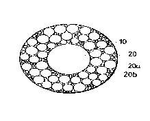
Fig. 2 is a sectional view of a second embodiment
of the insulated conductor according to the present
invention. In Fig. 2, the reference numeral 10 designates a
conductor, 20 designates an insulating lager which is a
coating of a mixture of microspheres and an energy
irradiation curable resin, 20a designates large-diameter
is microspheres, and 20b designates small-diameter microspheres.
In the following, the method of producing the
insulated conductor according to the present invention is
described with reference to one embodiment of the present
invention shown in Fig. 3.
2o A coating resin composition comprising a mixture of
microspheres of the same mean diameter and an energy
irradiation setting resin or a mixture of at least two kinds
of microspheres different in mean diameter and an energy
irradiation curable resin is applied to the outer surface of
z5 the conductor 4 fed out from a supply means designated by the
- 11 -
200286
numeral 3 in Fig. 3. The coating resin composition thus
applied is subjected to irradiation of energy, such as heat,
ultraviolet rays, an electron beam, or the like, supplied
from a resin hardening means 6, so that the coating resin
s composition is hardened to form a coating on the conductor 4
to thereby prepare an insulated conductor 7 according to the
present invention. The reference numeral 8 designates a
takeup means. The resin coating device 5 is the means by
which the coating resin composition containing microspheres
io and having a relatively high viscosity can be uniformly
applied. Known techniques, such as a technique of coating by
use of a pressure die, a technique of dipping by use of an
open die, and the like, can be used as the resin coating
device 5.
is How such an insulated conductor, which is small in
diameter and low in capacitance and which could not have been
realized in the prior art, can be realized by the present
invention is explained.
In order to explain the operation of the present
2o invention, the relation of the void ratio and the dielectric
constant will be described. The void ratio V is measured by
a density method and calculated by the following equation
(1).
(Po - P) ~ Po x 100.($) .....(1)
- 12 -
2005286
po represents the density of base resin, and p represents the
density of microsphere-containing resin.
It is well known that the dielectric constant, E,
of a microsphere-containing resin composition is determined
s by the dielectric constant el of the base resin, the
dielectric constant cz of a gas contained in the microsphere,
and the void ratio V produced by mixing the microspheres in
the base resin, and that the dielectric constant E is
represented by the following equation (2), when shell
io thickness of the microsphere is very thin and the dielectric
constant of the shell material is negligible.
Zsl + EZ - ZV( al - E2)
E - ~1 ~ ' ..... (2)
2~1 + ~Z + v( E1 - EZ)
1s Accordingly, desired voids can be formed stably in
the coating layer by selecting the material for forming the
microspheres, the void ratio thereof, the content of the
microspheres in the resin composition, and the material for
the resin composition, respectively, and it is therefore
2o possible to form an insulating layer having a desired
dielectric constant.
To establish the dielectric constant E to be a low
value not larger than 1.60, which is a target of the present
invention, the dielectric constant E1 of the base resin must
- 13 -
200526
be selected so as to increase the void ratio to a value
larger than 40~ because the lowest dielectric constant of all
resin, which fluorocarbon resin has, is 2.
In the case where the base resin is required to be
subjected to a high temperature for hardening, there is a
risk that the gas contained in the microspheres may expand
and contract and that the microspheres may become deformed
with the result that the void ratio cannot be maintained. On
the contrary, where ultraviolet-ray curable resin is used as
io the energy irradiation curable resin in the present
invention, the microspheres which help give the resin a
low-dielectric constant can be used because it is not
necessary to heat the ultraviolet-ray curable resin to harden
it. Also, an added way of attaining a very low dielectric
is constant in the resin is by selecting a resin with an
intrinsically low dielectric constant as the energy
irradiation curable resin.
Because the microspheres have a mean diameter
within a range of about 1 to about 100 ~.un and a shell
2o thickness not larger than 0.5 arm, voids can be formed
securely even if the coating is made of a thin film.
Accordingly, it is possible to produce an insulated conductor
capable of high-speed transmission in which the capacitance
of the insulating layer is not larger than 1.60, which would
2s not have been possible in the prior art products, even where
- 14 -
200586
the thickness of the insulating layer is not larger than 200
~.m .
Further, according to the present invention, an
energy irradiation curable resin composition containing
s microspheres is applied and then hardened through energy
irradiation, such as heat, ultraviolet rays, an electron beam
or the like. Accordingly, the manufacturing speed can be
improved greatly, compared with the prior art means of either
foaming a thermoplastic resin or winding up a tape.
. Because the insulating layer is formed of a coating
of a resin composition having a dielectric constant which is
predetermined by selecting the content of the microspheres in
the resin composition and the material for the resin
composition as described above, it is possible to avoid
~5 variations in capacitance due to instability of the
manufacturing process. Accordingly, it is possible to easily
manufacture insulated conductors of stable quality.
Further, because the resin composition contains
either microspheres all equal in mean diameter or
2o microspheres of at least two different mean diameters, both
of which are selected from microspheres having a particle
diameter of from 1 to 100 Vim, the present invention has a
further advantage in that the surface of the insulating layer
can be made much smoother as compared to the prior art.
- 15 -
... 2p0~~ap
EXAMPLE 1
Isobutane gas-containing vinylidene chloride-
acrylonitrile copolymer resin microspheres having a 40 ~m
mean diameter and a 0.05 um shell thickness (made by
. s EXPANCELL Co.), and an ultraviolet-ray curable resin
(dielectric constant: 2.50) mainly containing fluoroacrylate
of S00 cps viscosity were mixed in the volumetric proportion
3 . 1 and dispersed with stirring to thereby prepare a
coating resin composition having a viscosity of 8500 cps.
. The outer surface of silver-plated copper wire
having a 150 ~m external diameter was coated with the
prepared coating resin composition by use of a pressure-die
coating apparatus and then the coating is hardened with
radiation by use of an ultraviolet ray hardening apparatus
is consisting of a mercury lamp to thereby prepare an insulated
conductor having a coating thickness of 100 um and an
external diameter of 350 N.m according to the present
invention.
When the void ratio of the insulating layer of the
2o insulated conductor was measured by a density method, it was
70%. When the dielectric constant thereof was measured at a
frequency of 1 MHz, it was 1.38. When the fracture
elongation of the insulating coating of the insulated
conductor was measured, it was 50 %. Even though the
25 insulated conductor was wound on a 1 mm ~ mandrel, the
- 16 -
2005286
coating was not broken. In short, the insulated conductor
was flexible enough for practical usage.
EXAMPLE 2
Air-containing phenol resin microspheres having a
s 20 ~m mean diameter and a 0.1 ~m shell thickness, and an
ultraviolet-ray setting resin (dielectric constant: 3.45)
mainly containing urethane acrylate of 700 cps viscosity were
mixed in the volumetric proportion 3 . 1 and dispersed with
stirring to thereby prepare a coating resin composition
io having a viscosity of 9000 cps.
The outer surface of silver-plated copper wire
having a 150 ~m external diameter was coated with the
prepared coating resin composition by use of a pressure-die
coating apparatus and then hardened with irradiation by use
i5 of an ultraviolet-ray hardening apparatus with a mercury lamp
to thereby prepare an insulated conductor having a coating
thickness of 150 N.m and an external diameter of 550 ~m
according to the present invention. The void ratio of the
insulating layer of the insulated conductor was 70%. The
2o dielectric constant thereof was 1.60 (at a frequency of 1
MHz).
When the fracture elongation of the insulating
coating of the insulated conductor.was measured, it was 50~%.
Even though the insulated conductor was wound on a 1 mm ~
- 17 -
200586
mandrel, the coating was not broken. In short, the insulated
conductor was flexible enough for practical usage.
EXAMPLE 3
Air-containing glass microspheres having a 10 ~m
mean diameter and a 0.1 um shell thickness, and a
thermocurable resin (dielectric constant: 2.70) mainly
containing silicone resin of 1000 cps viscosity were mixed in
the volumetric proportion 2 . 1 and dispersed with stirring
to.thereby prepare a coating resin composition having a
viscosity of 1200 cps.
The outer surface of tin-plated copper wire having
a 200 um external diameter was coated with the prepared
coating resin composition by use of a pressure-die coating
apparatus and then hardened by use of a heat hardening
i5 furnace of from 300 to 400°C to thereby prepare an insulated
conductor having a coating thickness of 150 um and an
external diameter of 550 ~m according to the present
invention. The void ratio of the insulating layer of the
insulated conductor was 60~. The dielectric constant thereof
2o was 1.59 (at a frequency of 1 MHz).
When the fracture elongation of the insulating
coating of the insulated conductor was measured, it was 10 %.
Even though the insulated conductor was wound on a 5 mm ~
- 18 -
2005286
mandrel, the coating was not broken. In short, the insulated
conductor was flexible enough for practical usage.
Example 4
Isobutane gas-containing vinylidene chloride-
acrylonitrile copolymer resin microspheres having a 40 um
mean particle diameter (0.05 um shell thickness), isobutane
gas-containing vinylidene chloride-acrylonitrile copolymer
resin microspheres having a 8 um mean particle diameter (0.05
um_shell thickness), and an ultraviolet-ray setting resin
(dielectric constant: 3.45) mainly containing silicone
acrylate of 500 cps viscosity were mixed in the volumetric
proportion 2.2: 0.8 . 1 and dispersed with stirring to
thereby prepare a coating resin composition having a
viscosity of 9000 cps.
i5 The outer surface of silver-plated copper wire
having a 200 ~m external diameter was coated with the
prepared coating resin composition by use of a pressure-die
coating apparatus and then hardened with radiation by use of
an ultraviolet-ray hardening apparatus consisting of a
2o mercury lamp to thereby prepare an insulated conductor having
a coating thickness of 100 ~.m and an external diameter of 400
um according to the present invention. When the void ratio
of the insulating layer of the insulated conductor was
measured by a density method, it was 71 %. When the
- 19 -
200586
dielectric constant thereof was measured at a frequency of 1
MHz, a very low value of 1.55 was obtained.
COMPARATIVE EXAMPLE
One kind of isobutane gas-containing vinylidene
r
chloride-acrylonitrile copolymer resin microspheres having a
40 ~m diameter (0.05 yam shell thickness), and an
ultraviolet-ray curable resin (dielectric constant: 3.45)
mainly containing silicone acrylate of 500 cps viscosity were
mixed in the volumetric proportion 3 . 1 and dispersed with
io stirring to thereby prepare a coating resin composition
having a viscosity of 9500 cps.
Similarly to the Example 1, the outer surface of
silver-plated copper wire having a 200 dun external diameter
was coated with the coating resin composition thus prepared
~s by dispersion of the microspheres having the uniform particle
diameter, and then hardened by use of an ultraviolet-ray
hardening apparatus to thereby prepare an insulated conductor
having a coating thickness of 100 ~.!m and an external diameter
of 400 ~m (Comparative product).
2o The void ratio of the insulating layer of the
insulated conductor was 65%, and the dielectric constant
thereof was 1.80. In short, the insulated conductor has a
relatively low void ratio and a relatively high dielectric
constant compared with that of Example 4.
- 20 -
2005286
As described above, according to the present
invention, a thin-film coated insulated conductor which is
small in diameter but low in capacitance can be manufactured
stably with no variations in capacitance due to the
s manufacturing process and with a speed higher than the prior
art. The resulting insulated conductor has capacitance of a
designed value and has a smooth coating layer surface.
According to the present invention, a
small-diameter but low-capacitance insulated conductor in
which the dielectric constant of the coating layer is not
larger than 1.60 when the thickness of the insulating layer
is not larger than 200 um can be put into practical use,
though such an insulated conductor could not be obtained in
the prior art.
is Accordingly, the range of its use as a high-speed
transmission insulated conductor requested for high-density
signal transmission line in medical measuring machines,
computer measuring machines and the like can be enlarged
remarkably.
- 21 -