Note: Descriptions are shown in the official language in which they were submitted.
X0al~;395~
The present lnventlon relates to a double-stage
phase-diversity receiver for use ln not only coherent
optical fiber communlcations employing an optical fiber
but also, electrical communications, and radio wave
communications and light wave communications that use
spatial propagation.
Receivers used in coherent optical fiber communica-
tions are basically classified into two schemes, a
heterodyne scheme and a homodyne scheme. In the
heterodyne scheme with a very high speed of several
Gbits/sec, the intermediate frequency (IF) becomes lo
to 20 GHz, which makes it difficult to realize high-
performance receivers due to restriction on the fre-
quency response characteristic of a photodetector or
microwave circuit technology. In the homodyne scheme,
by way of contrast, although a light source is required
to have a narrow spectral width, the above difficulty
can be avoided because optical signal is converted
into a baseband signal. In this respect, research on
this homodyne scheme has recently been accelerated with
improvement of light sources. Further, attention has
been paid to phase-diversity scheme in which the
requirements for optical phase stability on laser diodes
for use in transmitter and for or local oscillator in
receiver are much relaxed. In there scheme, as well as
the homodyne scheme, however, (a) it is not possible to
compensate in the receiver the delay distortion produced
~0053~
by group delay of optical fibers while this compensation
is possible in the heterodyne scheme, and (b) it ls
technically more difficult to realize coherent ASK
(Amplitude Shift Keying) or PSK (Phase Shift Keying)
demodulators in baseband than in intermediate frequency
(IF) range. Of these intrinsic limitations to perfor-
mance of the phase-diversity scheme, the limitation (b)
can be overcome, as recently proposed, by converting
baseband signal into an intermediate frequency, before
demodulation. Yet no solution has yet been proposed to
the first limitation (a).
Silica fiber has the lowest transmission loss in
1.55-~m wavelength band, but in this wavelength band, a
relatively large group delay distortion occurs in the
signal waveform, because of wavelength dispersion. This
group delay distortion restricts the transmission speed
or the transmission distance particularly in signal
transmission at a high speed of several Gbits/sec. As a
solution to this shortcoming, dispersion-shifted fibers
or dispersion-flattened fibers may be employed to reduce
the wavelength dispersion. These optical fibers,
however, have higher transmission loss; the former type
fibers has a narrow region where the dispersion is
negligible and the latter fibers are difficult to
manufacture.
Accordingly, lt is an ob~ect of the present
lnventlon to provlde a double-stage phase-dlversity
, . . . .
X()OS3~
receiver which can simultaneously realize the merits of
the homodyne scheme and heterodyne scheme, whereby a
high-speed signal transmission can be facilitated by
compensating the group delay of optical fibers, and
utiliæing the narrow band property of the homodyne
scheme.
According to the present invention, the communica-
tion signal is divided into a plurality of divided
signals with which a plurality of first-stage local
oscillator signals having predetermined phase relation
is mixed to provide a plurality of electrical signals
which are up-converted by a plurality of second-stage
local oscillator signals having predetermined phase
relation, these up-converted signals are added, and the
result of the addition ls demodulated similarly to a
heterodyne scheme.
Fronted detection equivalent to that in homodyne
scheme and demodulation similar to the heterodyne scheme
are attained, and only the merits of both schemes can
be reallzed, whlle the demerits of both schemes are
removed.
The narrow band property of homodyne scheme is
retained while the demodulation can permit a compensa-
tlon for the group delay distortion which is originated
from the wavelength dispersion of optical fibers
similarly to the heterodyne scheme.
Thls lnvention can be more fully understood from
20~5399
the following detailed descriptlon when taken ln
con~unction with the accompanying drawings, ln whlch:
Flg. 1 is a conceptual diagram for ~xplaining the
present invention:
Fig. 2 is a block diagram of a double-stage phase-
diversity optical receiver according to the first
embodiment of this invention;
Fig. 3 is an equivalent circuit diagram for
explaining the same embodiment;
Fig. 4 is a diagram for explaining the effect of
the same embodiment;
Fig. 5 is a block diagram of a double-stage phase-
diversity receiver according to the second embodiment of
thls invention;
Fig. 6 is a block diagram of a double-stage phase-
diversity receiver according to the third embodiment of
this invention;
Fig. 7 is an experimental result in a double-stage
phase-diversity optical receiver according to the first
embodiment and shows the power spectrum of the added
up-converted intermediate frequency signals under no
modulation;
Fig. 8 is another experimental result and shows the
power spectrum of the added up-converted intermediate
frequency signals under FSX modulation;
Fig. 9 ls another experimental result and shows
the power spectrum of the heterodyne demodulated
XC~053~9
intermediate frequency signals under FSK modulation;
Flg. 10 is another experlmental result and shows
the measured bit error rate as a function of received
signal optical power; and
Fig. 11 is an experimental result in a double-
stage phase-diversity radio wave receiver according to
the concept of the invention and shows the power
spectrum of the added up-converted intermediate
frequency signals.
Preferred embodiments will be described below
referring to the accompanying drawings.
Fig. 1 presents a conceptual diagram of a double-
stage phase-diversity receiver embodying the present
invention. The illustration involves coherent optical
fiber communications. When coherent ASK or PSK
modulation is considered, a signal light input to the
double-stage phase-diversity receiver is expressed
by:
f(t) = v(t) cos (~st + ~) ... tl)
where ~S ls an angular frequency of a carrier, and ~
ls the phase difference between the carrier and a local
osclllation signal, which is constant during a bit
interval T (reciprocal of a bit rate).
The signal is divided into two signals with which
first-stage local oscillation signals having a phase
dlfference of 90 and an angular frequency ~LO are
mixed at mixers. The mixed signal have currents il(t)
~00~;39~
-- 6
and i2~t). These currents are given by the followlng
equations:
i1(t) = sv(t) cos (~OFFt + ~) ... ~2)
i2(t) = -Sv(t) sin (~OFFt + ~) ~' (3)
where S is a constant representing the mixing efficiency
of the mixers and ~OFF is an offset angular frequency
for applying automatic frequency control (AFC). The
latter element is given by:
~OFF = ~S - ~LO
Two electrical baseband signals obtained through
the above the mixers are amplified if necessary and up-
converted by second-stage local oscillator signals
having an angular frequency ~IF, and a phase difference
of soo and resulting intermediate frequency (IF). The
currents i1'(t) and i2'(t) are given by the following
equations:
il'(t) = 2 Sv(t) cos {(~OFF + ~IF)t + ~)
+ 2 Sv(t) cos {(~OFF - ~IF) t - ~}
(4)
i2'(t) = 2 Sv(t) cos {(~OFF + ~IF)t + ~}
~ 2 Sv(t) cos {(~OFF - ~IF)t - ~}
... (5)
These two IF currents are inputs to an adder
whlch in turn outputs an added result io. This added
output io ls given by:
Io(t) = il'(t) + 12 (t)
= Sv(t) cos {(~OFF + ~IF)t + ~ -- (6)
.. ~
"
X00539'~3
The output iott) is exactly the same as the current
attained when the signal is sub~ected to heterodyne
detection with the intermediate frequency ~OFF ~ ~IF~
Therefore, supplying this added output io(t) to an
equalizer 1 having a predetermined transfer function can
permit compensation for the group delay. The compen-
sated result ls demodulated by an ordinary heterodyne
demodulator 2, which can provide a baseband signal.
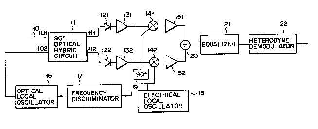
Fig. 2 is a block diagram illustrating the first
embodiment of the present invention.
Referring to this diagram, numeral 11 denotes an
optical hybrid circuit which has two input ports; the
first input port receives signal light from an optical
fiber 10, and the second input port receives a optical
local oscillation signal from an optical local
oscillator 16. The optical local oscillation signal
from the local oscillator 16 is sub~ected to frequency
control by a frequency lock loop which has a frequency
dlscriminator 17.
The optical hybrid circuit 11 has two output ports
from which mixed llghts acquired by mixing the signal
light with two optical local oscillation slgnals having
a mutual phase dlfference of 90. Of the two outputs
from the optical hybrid circuit 11, output 111 has a
phase delay of 90 as compared with that of the output
112. These outputs are supp~ied to associated mixers
141 and 142 respectively through a circuit of
,
201)S3't9
a photodiode 121 and an amplifier 131 and a circuit of a
photodiode 122 and an amplifier 132.
The mixer 141 receives a electrical local oscilla-
tion signal from an electrical local oscillator 18,
which has its phase delayed by soo via a phase shifter
19. This electrical local oscillation signal is multi-
plied by the output of the amplifier 131. The same type
mixer 142 receives a electrical local oscillation signal
directly from this electrical local oscillator 18. This
electrlcal local oscillation signal is multiplied by the
output of the amplifier 132.
The outputs of the mixers 141 and 142 are supplied
to an adder 20 respectively through amplifiers 151 and
152, and are added there. The result of the addition is
given to an equalizer 21. This equalizer 21, having a
predetermined transfer function already set therein,
compensates for a group delay of the optical fiber 10.
The output of the equalizer 21 is supplied to a
heterodyne demodulator 22 for demodulation, and a base-
band signal is output from this demodulator 21. With noconslderation being given to the group delay of the
optical fiber 10, however, the equalizer 21 can be
omitted.
Fig. 3 presents an equivalent circult diagram for
explaining the operation of equalization delay
distortion in this embodiment.
Signal light fin(t) input to the optical fiber 10
.
ZO()~:;3~3
is expressed by:
fin(t) = IOA ~P) COS {(~S + p)t + ~ + ~(p)} dp
+ IOB (P) COS { (~S - p)t + ~ - ~(p)} dp
+ C COS ( C~St + ~ ) . . . ( 7 )
In this equation, the third term represents a optical
carrier, and the first and second terms an upper side-
band and a lower sideband, respectively. Variables
A(p), ~(p)~ B(p), and ~(p) give the sideband waveforms
and phases, A ( P ) and B(p) are illustrated in Flg. 3.
With the transfer function of the optical fiber 10
being H ( ~ ) which is expressed by
¦H(~) ¦ - G(~), arg H(~ (8)
then signal light fout given by the following equation
is at the output end of the optical fiber 10.
fOUt(t) = IOG (~S + P) A(P) COS ~ (~S + p)t + ~
~(P) + ~(~s + P)} dp
+ I~G (~S - P) B(p) cos {(~s - p)t + ~
- ~(P) + ~(~s - P)~ dp
+ CG(~S) cos {~st + ~ + ~(~s)} (9)
2~ This signal llght is supplied to the optical hybrid
circuit 11 and is divided into two components, which
result output currents il(t) and i2(t) at photodlodes
121, 122. These currents are given by the following
equations:
.
2C~OS39`'3
- 10 --
i1(t)/S = IOG (~S + P) A(p) cos ~(P + ~OFF)t + ~
~(P) + ~(~s + P)} dp
+ IOG (~S - P) B(p) cos ~(P ~ ~OFF)t ~ ~
+ ~(P) ~ ~(~s - P)} dp
5+ CG ( ~S ) COS { ~OFFt + ~ + ~ ( 'oS ) }
... (10)
i2(t)/S = -IWOG (~S + P) A(p) sin {(P + ~oFF)t + ~
+ ~(P) + ~(~s + P)} dp
+ JWOG (~S - P) B(p) si~ {(P ~ ~OFF)t ~ ~
+ ~(P) ~ ~(~s - p)} dp
- CG(~S) sin {~oFFt + ~ + ~(~s)}
... (11)
where W is the band width of the detectors.
In the equation (10) the three terms have the same
sign, while in the equation (11) only the second term
has a different sign from the first and the third. This
means that an in-phase sideband, even when folded over,
has the sign unchanged whereas a quadrature-phase side
wave band has the sign inverted.
Given
20a(t) - ¦OG (CDS + P) A(P) COS { (~IF + P + ~OFF)t
+ ~ + ~(P) ~(~s + P)} dp ... (12)
a'(t) - ¦OWG (~S + P) A(P) COS {(C~IF - P - ~OFF)t
~ (P) ~ ~(~s + P)} dp ... (13)
b(t) - ¦oG (~s - p) B(p) cos {(~IF + P ~ ~OFF)t
~ + ~(P) + ~(~s - P)) dp ..... (14)
b'(t) - ¦WG (~S - P) B(p) cos {(~IF ~ P + ~OFF)t
+ ~ ~ ~(P) + ~(~s - P)~ dp ... (15)
' ~ ' , ...
20~)~i3!~
c(t) - CG~S) cos ~IF + ~OFF)t + ~
+ ~s)) ... ~16)
cl(t) _ CG(~S) cos {(~IF ~ ~OFF)t ~ ~
~ ~(~s)~ 17)
then the outputs i1'~t) and i2'~t) of the mixers 141 and
142 can be expressed by the following equations:
il'~t~/S = a~t) + a~t) + b(t) + b'(t)
+ c(t) + c~t) ... (18)
i2'(t)/S = a(t) - a~(t) - b(t) - b'(t)
- c~t) - cl(t) ................... (l9)
These outputs i1'~t) and i2'~t) are supplied to the
adder 20 for addition. The output io of this adder 20
is expressed as follows:
io~t)/S = a(t) + b'(t) + c(t) ... (20)
Accordingly, with the transfer function of the equ-
alizer 21, Ho(~)~ being given by
Ho(~) K H-l(~ + ~S - ~IF - ~OFF) ... (21)
then, the delay of the optical fiber can be compensated
for, as should be obvious from the equations (12), (15)
and (16). Since ¦HO(~)I can be assumed to be constant,
the following should only be satisfied:
IHO(~)I = const ... (22)
argHO(~) = -argH(~) ... (23)
In other words, according to the homodyne receivers
and conventional phase-diversity type receivers, as is
illustrated in Fig. 4, the upper and lower side bands of
a signal are folded in the baseband, which makes it
., ,
, :, : ' '
.
,,
~, . .
..
'' ' ' :
X()()S3~.3'.1
imposslble to compensate the delay of the optical
fiber, whereas according to the double phase dlversity
receiver, the upper and lower side bands can be sepa-
rated again when the base band signals are up-converted
to the intermediate frequency band, and added, thus
ensuring compensation for the delay distortion of the
optical fiber as per the heterodyne scheme.
For a wavelength band (1.55 ~m) of the abnormal
dispersion region of silica optical fibers, the delay
compensation can be effected by using as the equalizer
21 a medium having a flat amplitude characteristlc and
having a positive dispersion, such as a strip line. on
the contrary for longer wavelength band (equal to or
less than 1.3 ~m~ having the normal dispersion, the
output io of the adder 20 in the equation (20) should
consist of a~(t)~ b(t) and c~(t). This may be done by
changing the connection of the local oscillator 18 or
changing the polarity of one of the inputs to the adder
20.
In addition, arg H(~) is inserted into the equa-
tions (9) to (17), the first term of arg H(~) presents
a uniform time delay and the second term represents the
dispersion.
The reception scheme of such a double phase diver-
sity recelver produces the effects as shown in the fol-
lowing table given in comparison with the results of
other receiving schemes.
. .
200539~
-- 13 --
~ ~ C ' q~ ~
U~ ~ lR ~O ~,a o E C
I ,, ~ o 5~ ~ a) ,,
a~ I tq ~ ~ ~ a) a) a~ ~ ~
~1 9) ~ E ~ C ~q C
~Q ~ ~ ~ ~ ~ 0 ~:~ o
o ~ ~ U~ ~~ ~ ~ Cq ,C ~ ~q U
Q~:4Q
.
~ ~ ~o~ ~ o
~q ~ o o~ ~ o
h ~1 0 a) a~ O
a) ~D a) a) t~ 0 ~1 ~ ~ ~ ~~ C u~
E; ~ C rl 3 ~ ~ ~ ~a ~ a~ :>
,~ ~ ~ o ~ ~ ~ u~
rn
~ V 1 ~ ~o
E a~ n~C ~ o o
~ ~ . ~n
. a~ .
a
a) ~ ~ 1 ~ ~ h
S O O ~ ~ rQ O ~ O O ~ S-l
3 ~: lQ v-~
O o :~ ~ ~ C ~ ~ O O :~
O ~1 C ~q ,5:1 ~ 0 ~q O ~
~ o ~ a~ u~ 1 0 U~ O
~ m c ~ ~ ~ ~ ~ c ~
0 C 41 0 ^~ h ~) 0 C --U~ O
~ C ~ ~ O IJ -I O ~ O
:1: ~ ~ ~ --E~ --U ~-I
C ~
om ~ ~ ~ ~ o
~ ~'aO ~ ~
t) ~ U~ ~ ~ ~ 0
a
~J ~1 3 ~ ~q 0 .c: 0
~1 0o o a) :~ ~ a~
~ ~ q :~ _
~ / ~1 ~ ~ h I h ~1 ~1
~' / ~ ~ ~ ~ ~ ~ O
~/ ~ 1 ~1 ~ rl ~C ~ ~
W O bq ~ O ~ ~ ~ ~ a) u o
E ~ C ~ ~ d ~C~ ~q a) C
/ ~a~ ~ ~ a) ~ 0 a~ 1 0 ~-rl
/ ~ P: ~q-,l ~ m
/
.
:.
- ' ' ' , .
' '' ''
,
200S399
- 14 --
--O--Q I O O O
,~ ~ O rl O ~1 ~1
u~ ~ ~a ~ ~ ~ :~ o ~ o
I ~1 Vl ~ 0 ~ C~ ~ F .~ ~ ~1
a~ I ~ o u~ u~ o u o~
~ J ~ U ~ 5 ~ U~
n ~q a) ~ Q o
~1 ~ bq O O O O ~ ~ ~ ~ ~ a) Gq a
'~ l¢ ~Q 0 E~ ~1 E ~R U~ 5~ O ~ ~ 1
. . ~
a~ ~ _ a) l IIQ I
~1 ,~ ~ .,1 .,1 E~ O ~ ~q ~
,1 ~ ~ ~ h O O ~ ~ U~ :~ O ~ ~1~ O
~q ~ E a~ ~ ~O 1~ h
o ~ ~ ~1 ,a u ~ 1 ~ o o ~.) ~ ~ o ~1
~q ~ ~ ~q u ~c ~ ~ ~ ~ 0 ~ P~
0 :, ~ o x ~q ~ e,~
d ~1 ~ 0 rl ~Q 0 0 0 ~ O H~a 0 a~ 0 C ~ ~Q
u~ ~ tq 5~ ~J 0 ~ n~ s~
a~ ~1 d ~1 a) ,1
C~ 5~ ~ .Q ~0 ~U ~1 ~Q
C Q) ~ O
o ~1 ~q u ~4 ~ ~ ~ a~
E ~ o x u~ 0 ~ ~ E ,1
. ~ m ~Q ~ o H Q
:~
_ :
,1 o I E~
C ~ ~ O ~ 0 $
~1
~q ~ Q~ c
~o o 0~ o ~
0 ~I C C~ ~ , od ~Q
~q ~ 0 ~ 0 ~
. .
o ~ ~a ~1
~ ~ ~q 0 ~ 0C ~ 0 ~Q
U U C~l U~ 0~ lQ
a~ C ~l o
~, ~ ~ ~ ~a o h ~q tJI 0
c c o ,l ,~ 0-~1 ~
O ~ ~ ~ 5~ ~q 0 H
o / o a~
~/ Q0 a~ ~:~C~ ~r-10
0/ ~ rl~ O ~ 0 0-rl
UY ~q 5 C O ~ O rl O ~1 :~ ~ d
/ E~ ~q ~ o ~ u~ ~ ~ C O tJI 0 ~
/ 0 O 0-~1 O O a~ 0 U ~ liil N O
/ H P~ 1~ Q
~ .
.
20053'~
- 15 -
Let us now check the effects of double-stage phase-
diviersity scheme item by item.
(1) Reception Sensitlvity
Since the double-stage phase-diversity receiving
scheme divide signal light into more than two parts
prior to detection, its reception sensitivity is lower
than that of the idealistic homodyne scheme, but can be
kept at substantially the same receiving sensitivity of
the heterodyne scheme.
(2) Required Detector Band
Similar to the homodyne scheme and phase diversity
scheme, the optical current after detection is in the
baseband, and the required detector band can be half the
bit rate from the Shannon's theorem.
(3) Requirement for Width of Laser Spectral Line
The requirement for the width of the laser spectral
line is determined by the demodulation scheme, not the
detection scheme. The requirement is very severe for
the homodyne scheme in which detection and demodulation
are unified. Since the double-stage phase-diversity
receiving scheme employs the heterodyne demodulation,
however, the requirement is the exactly the same as that
of the heterodyne scheme.
(4) ~odulation Scheme
Due to the use of the heterodyne modulation, the
double-stage phase-diversity receiving scheme can deal
with all of ASK, FSK (Frequency Shlft Keylng) and PSK.
20053'.~9
- 16 -
(5) Demodulatlon Scheme
Slnce the double-stage phase-diversity recelvlng
scheme employs the heterodyne demodulation, it can use
the same demodulator as the heterodyne scheme. In
addition, according to the double-stage phase-diversity
reception scheme, the intermediate frequency is not
restricted by the band of the detector, so that this
scheme can also employ a PSK synchronous demodulation
whose use is difficult in the heterodyne scheme.
(6) Delay Equalization
This can be done in the same manner as done in the
heterodyne scheme.
(7) Other
The phase diversity scheme requires the same number
of detectors and demodulators as the number of ports,
whereas the double-stage phase-diversity receiving
scheme requires only one demodulator and the same number
of detectors as that of the ports.
Fig. 5 illustrates the second embodiment of the
present inventlon, which is a multi-port (K ports)
double phase diversity reception scheme.
An optical hybrid circuit 11 has K output ports to
which a circuit of a photodiode 121, ampllfier 131 and
mlxer 141, a circuit of a photodiode 122, amplifier 132
and mixer 142, .. , and a circuit of a photodiode 12X,
amplifier 13K and mlxer 14K are respectively connected.
Mlxers 141, 142, ... and 14K receive a electrical local
.
.
.,
~;
' ~
~OOS39'~3
- 17 -
oscillation signal having a phase difference of
2~(K-l)/K via a phase shifter 19 from an electrlcal
local Gscillator 18. The outputs of these mixers 141,
142, ..., and 14K are supplied respectively through
amplifiers 151, 152, .... and 15K for addition. Since
the other circuit arrangement is the same as the one
shown in Fig. 2, the same reference numerals as used to
specify the identical or corresponding elements in the
second embodiment, thus omitting their description.
In this case, with K 2 3, the first-stage local
oscillation signal and second-stage local oscillation
signal given to the k-th port are cos (~s'+2nk/K) and
cos (~IFt+2~k/K), the light current iK(t) acquired
through the optical hybrid circult 11 becomes
15iK(t) V(t) cos (~oFFt + ~ - 2~k/K) ......... (24)
and the current iK'(t) given by the individual mixers
141-14K becomes
iK'(t) v(t) cos {(~IF + ~OFF)t + ~
+ V(t) cos {(~IF - ~oFF)t + ~ + 4~k/K}
... (25)
Thls yields the output io(t) of the adder 20 expressed
as
io(t) ~ Kv(t) cos {(~IF + ~OFF)t + ~} -- (26)
The results are the same as those obtained by the
aforementioned.
Fig. 6 illustrates the third embodiment of this
invention.
.
.
' :
20U53'~9
This embodiment ls a comblnation of a polarizatlon
diversity and a double-stage phase-diversity receiver
provided for each of two orthogonal polarizations
propagated through the optical fiber. In this case, the
individual double phase diversity outputs after under-
going modulation in demodulators 22 are added together
by an adder 23, which in turn outputs the added result.
Since the other circuit arrangement is the same as the
one shown in Fig. 2, the same reference numerals as used
to specify the identical or corresponding elements in
the second embodiment, thus omitting their description.
Although the foregoing descriptions of the individ-
ual embodiments have been given mainly with reference to
coherent optical fiber communications, the present
invention can be widely applied to optical communica-
tions involving spatial propagation as well as electri-
cal communications, radio-wave communications, radars,
general instrumentation technology and the like which
use electrical signals of a long wave, medium wave,
short wave, ultrashort wave, millimetric wave, sub-
millimetric wave, etc.
Utilizlng the setup shown in Fig. 2, an experiment
is carried out. An FSK modulated optical data signal of
100 Mbit/s one-zero pattern with a frequency deviation
of about 600 MHz is generated as output optical signal
ln a DFB semiconductor laser with a narrow linewidth of
10 MHz in 1.30 ~m wavelength range by injecting
ZO~)53'`~
-- 19 --
electrical current pattern correspondlng electrlcal data
signal. The optical slgnal ls fed into a goo optical
hybird as shown by lOl in Fig. 2, through signal mode
optical fiber, and local osclllator optlcal slgnal ls
fed into the hybrid as shown by 102 in Fig. 2. The
local optlcal osclllator signal is generated ln the same
type of semiconductor laser with almost same electro-
optical performances as that for the data signal. Both
lasers are temperature-controlled to ~0.01K and the
frequency of the local oscillator is adjusted near the
center frequency of the modulated signal FSK spectrum.
Isolators are inserted in front of the two lasers. An
N~ filter ls lnserted in the slgnal path to simulate a
fiber. The goo degree optical hybrid conslsts of a
A/4-plate and polarlzation beam splitter (PBS). The
front-end is a phase-dlverslty receiver using InGaAs PIN
photodetectors and hlgh-lmpedance-type baseband
ampllfiers. The local osclllator power measured at the
photodetector surface is -3 dBm. In the second-stage
~0 phase-dlverslty frequency up-conversion, the baseband
signals are up-converted to 650 MHz (central frequency)
uslng two double-balanced mixers. The two up-converted
lntermediate frequency slgnals are added by means of a
reslstive combiner, and fed to a conventional FSK
heterodyne signal-fllter demodulator consisting of a
band-pass filter (center: 1 GHz, bandwidth: 400 MHz), an
envelope demodulator, and a low-pass filter (bandwidth:
.... . :
~ . " .
'- ' ~ ', .
200S39~
- 20 -
50 MHz). Fig. 7 shows the signal power spectrum of the
added upconverted intermediate frequency with no
modulation. The offset frequency (the difference
between the optical signal and local oscillator
frequencies) is set to be lO0 MHz. The unwanted signal
which would appear at 550 MHz, if the cancellation is
not complete, is found to be suppressed at least 20 dB
below the signal at 750 MHz, demonstrating that the
double-sage phase-diversity (DSPD) scheme is functioning
as expected. The pure line spectrum at 650 MHz shows the
spuriously coupled local oscillator signal; this can
eventually be eliminated afterwards because it is outside
the pass band of the band pass filter. Fig. 8 shows the
signal power spectrum of the added upconverted inter-
mediate frequency under FSK modulation. This spectrumis found to be identical to that in a conventional
signal-port heterodyne receiver using the same system,
and shown in Fig. 9. The measured bit-eror rate (BER)
is shown in Fig. 10 as a function of the sum of the
received optical powers detected by two photodetectors
in the two branches. The BER of the heterodyne receiver
is also measured and shown for comparison in Fig. lO.
Theoretically, the sensitivities of double-stage phase-
diverslty and heterodyne schemes are equal, whereas
0~6 dB degradation ls observed. This degradation is
most probably due to imp~rfect phase and amplitude match
between the two branches.
,
~()0~;3~t9
- 21 -
A radio-frequency experlment is also performed.
An 1 MHz carrier is modulated by a 12 kHz slgnal having
a triangular waveform, and received by a double-stage
phase-diversity receiver. The receiver has a first-
stage oscillator frequency of 0.996 MHz and the mixedsignals are fed into low pass filters with cutoff
frequency of 160 kHz and are up-converted to inter-
mediate frequency using second-stage local oscillator
signals of 0.996 MHz. These intermediate frequency
signals are added.
Fig. 11 shows the power spectrum of the added
intermediate frequency (IF) signals. The upper and
lower sidebands are clearly separated, and the obtained
signal is nothing but what would be obtained as the
intermediate frequency signal in an ordinary heterodyne
receiver.
, .