Note: Descriptions are shown in the official language in which they were submitted.
2005~ 71.
FIELD AND BACKGROUND OF THE INVENTION
1 The present invention relates to the processing of
2 semiconductor wafers in plural chambers. As shown in our
3 commonly assigned U.S. Patent No. 4,715,921, issued December 29,
4 1987 and U.S. Patent Applications Serial No. 853,775, Filed
April 18, 1986, and Serial No. 115,774, Filed October 30, lg87,
6 the use of plural chambers to process semiconductor wafers
7 permits more efficient, rapid and flexible semiconductor wafer
8 plasma environment processing. In that disclosure the ability is
9 provided to address the wafers in an individual cassette to
different ones or multiples of processing chambers associated
11 with that one cassette.
12 In the use of multiple chambers it can occur that one or
13 more chambers must be serviced. Time is lost in the process of
14 repairing or converting those chambers to other functions due to
the extended period of time needed to bring chambers to the
16 vacuum state needed to process semiconductor wafers.
BRIEF SUMMAR~ OF THE INVENTION
17 According to the teaching of the present invention a multi
18 processing, multichamber system is provided in which processing
19 chambers associated with a multichamber multiprocessing facility
2QOS5~1
1 are readily exchangeable to minimize "down time" and in which the
2 use of buffer wafer storage elevator cassette systems is utilized
3 to expand the number of processing chambers and provide wafer
4 input and output access at intermediate points.
According to one embodiment of the invention, a cluster of
6 processing chambers are arrayed about a wafer transport. One or
7 more o the processing chambers is provided as a mobile system
8 which may be selectively attached and detached to the wafer
9 transport system without loss of the controlled environment
within the transport and other chambers and without loss of the
11 controlled environment within the mobile processing chamber
12 itself. Each mobile chamber is equipped with its own evacuation
13 capability along with the electronics for generating plasma,
14 sputtering or other processing conditions within the processing
chamber and with a gas feed system for supplying appropriate
16 environmental gases to the chamber. The mobile character of the
17 chamber permits the multichamber facility to continue to operate
18 without complete breakdown in the case where it is desired to
19 exchange one chamber for a chamber of a different processing type
or to repair a chamber. Additionally, by providing back-up
21 chambers in a pre-evacuated condition ready for selective
22 attaching to a multichamber facility, the long down time
23 necessary to pump down the system is avoided by keeping the
200~ j 71
1 remainder of the processing system at the environmentally
2 controlled, typically low pressure environment, while the
3 selectively attachable pre-evacuated chambers are attached and
4 decoupled at the appropriate controlled environment. This
necessitates the evacuation of only a small portion of unwanted
6 gases which typically enter the system or mobile chamber through
7 the docking mechanism that provides selective attachment of the
8 mobile chamber to the multichamber multiprocessing facility.
9 In another embodiment of the invention the flexibility of
multichamber multiprocessing facility is enhanced by coupling
11 plural such facilities through intermediate wafer buffer storage
12 cassette and elevator systems. Additionally, a wafer transport
13 path, contained within a closed environment, is provided between
14 elevators with an access elevator system along the transport path
to permit intermediate wafer input and output.
BRIEF DESCRIPTION OF THE DRAWING
16 These and other features of the present invention are more
17 fully described below in the solely exemplary detailed
18 description and accompanying drawing of which:
19 Fig. 1 is an overhead view of a multichamber ~ultiprocessing
-- 4
2005~
1 system having plural multichamber facilities and mobile
2 processing chambers with a wafer buffer storage cassette and
3 elevator system between multichamber facilities;
4 Fig. 2 lS an elevational partially interior partially
sectional view of a docked mobile chamber for use in the
6 embodiment of Fig. l;
7 Fig. 3 is an illustration of a wafer transport system for
8 transporting wafers between buffer storage cassette elevator
9 systems and providing access along the transport path for wafer
insertion and removal; and
11 Fig. 4 i5 a view of the transport mechanism within a
12 controlled environment enclosure of Fig. 3.
DETAILED DESCRIPTION OF THE INVENTION
13 The present invention contemplates a system for providing
14 multichamber multiprocessing of semiconductor wafers in which
individual processing chambers are mobile to permit easy exchange
16 of processing chambers without requiring the down time for
17 complete system evacuation and further for permitting flexible
18 extension of processing capabilities by joining multiprocessing
19 multichamber facilities through a wafer buffer storage cassette
and elevator system that may include intermediate buffer storage
21 that permits wafer insertion and removal from the overall
22 processing system.
2Q05r.~71
1 Such a system is illustrated in Fig. 1 in which a
2 multichamber multiprocessing facility 10 is connected to a second
3 such multichamber multiprocessing facility 12 through an
4 intermediate cassette system 14 which typically comprises a multi
wafer containing cassette and elevator for positioning each wafer
6 slot in the cassette at a point where it can be accessed by a
7 transfer arm contained within respective transfer mechanisms 16
8 and 18 of the multiprocessing facilities 10 and 12. Each
9 transport mechanism 16 and 18 is typically provided with a vacuum
pump 20 capable of evacuating at least the interior of the
11 transport mechanism 16.
12 Arrayed about each transport mechanism 16 are a plurality of
13 multiprocessing chambers. Those arrayed about the transfer
14 mechanism 16 are illustrative of a typical single multiprocessing
~ facility. As shown there processing modules 22 and 24 are of a
16 type which may be permanently associated with the transfer
17 mechanism 16 while processing modules 26 and 28 are mobile
18 processing modules, more fully illustrated below in Fig. 2.
19 Each of the chambers 22, 24, 26 or 28 are coupled to the
transport mechanism 16 through a valved access port and docking
21 mechanism comprising first parts 32 containing a slit access
22 valve, as more fully illustrated in Fig. 2, througll which a
23 semiconductor wafer may be passed from the transport mechanism 16
-- 6 --
.. , .,. .. , : .
,
'
200557~1
1 on an arm 34 into and out of the respective chambers 22, 24, 26,
2 28 (or mobile chamber 30 for mechanism 8) through a further valve
3 and docking mechanism 36 associated with each of the chambers 22,
4 24, 26, 28 (and/or 30 for mechanism 18). The cassette
elevator 14 is similarly coupled through a valve and docking
6 mechanism 38 of the same type associated with the transport
7 mechanism 16 and spacer collars 40 associated with the cassette
8 elevator 14. Because the cassette elevator 14 does not contain a
9 gaseous wafer processing environment it is normally unnecessary
that the spacer 90 have a valve associated with it, but a
11 spacer 40 is provided so that the distance between wafers in the
12 cassette 14 and the pivot point of arm 34 can be made the same as
13 the distance between that pivot point and the point at which
14 wafers are placed within each of the processing chambers 22, 24,
~ 26, 28, and 30.
16 Reference is fldditionally made to United States Patent
17 No. 4,715,921, issued December 29, 1987 and U.S. Patent
18 Applications Serial No. 853,775, Filed April 18, 1986 and Serial
19 No. 115,774, Filed O~tober 30, 1987 in which portions of the
structure of the Fig. 1 apparatus are additionally illustrated.
21 The details of mobile processing chambers 26, 28 and 30 are
22 illustrated more fully below with respect to Fig. 2.
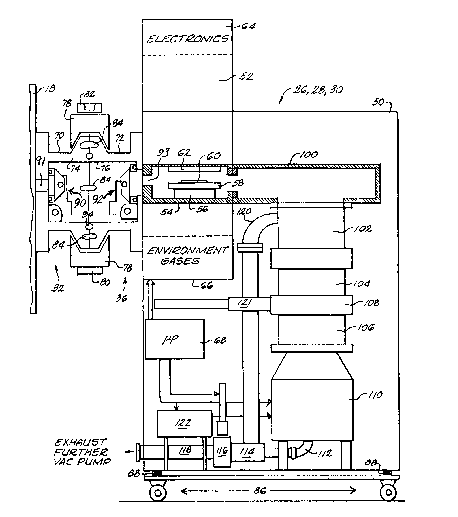
20055~1
1As shown in Fig. 2 each o~ the chambers 26, 28 and 30
2 includes a housing 50 in which a module 52 is installed and that
3 contains a chamber 54, having a pedestal 56 supporting a
4 cathode 58 on which a wafer 60 is typically placed ~elow an
anode 62 from which, in the example of plasma processing, an
6 electric field emanates to produce a plasma discharge for
7 processing of the wafer 60. The module 52 additionally includes
8 electronics 64 which in the case of plasma discharge provides the
9 appropriate field between the anode 62 and cathode 58 as known in
the art. The module 52 may also contains an environmental gas
ll control system 66 to supply appropriate etching gases in the case
12 of plasma etching or gases for other purposes as described
13 below. The control of the electronics and environmental gas
14supplies 64 and 66 is under the direction of a microprocessor 68
located within the housing 50.
16The module 52, in the specific illustration of Fig. 2, is
17 intended for plasma etching of the surface of the wafer 60.
18 Other modules can be provided that will employ other processing
19 technologies such as chemical vapor deposition, sputtering, rapid
thermal processing, rapid thermal annealing, plasma cleaning to
21 name a few, and utilizing technology and apparatus already known
22 in the art.
200557~
1 The module 52, as installed within the housing 50, mates,
2 for wafer exchange and transfer, with the wafer transfer
3 mechanism 18 through coupling and docking valves 32 and 36. In
4 particular each such valve includes a conduit 70 and 72 which are
fastened to the mechanism 18 and module 52 respectively. The
6 conduits 70 and 72 have outer beveled flanges 74 and 76
7 respectively which are joined through a quick connect band 78
8 typically hinged at a hinge 80 and coupled with a clamp 82.
9 Locating pins 84 are typically provided to accurately align the
conduits 70 and 72 and thus module 52 with respect to the
11 transfer mechanism 18 so that a wafer may be inserted through the
12 conduit 70 and 72 into the chamber 54 and onto the cathode 58.
13 To facilitate this ali~nment, the housing 50 rolls upon a
14 dolley system 86 which is adjustably supported from the base of
~ the housing 50 through adjustment screws 88. Conduits 70 and 72
16 are typically elongated in the dimension in out of the page in
17 order to accommodate the full width of a semiconductor wafer.
18 In order to seal the controlled environment within the
19 transfer mechanism 18 and within the chamber 54, valve
assemblies 90 and 92 are provided within the conduits 70 and 72
21 respectively to seal access ports 91 and 93 into the respective
22 interiors. Valves of this type are illustrated in the
23 above-identified, commonly assigned patent and applications.
~()05~71
1 Seals 94 may be additionally provided in the facing surfaces
2 of the conduits 70 and 72.
3 The interior of the chamber 54 is connected through a
4 manifold 100 through a series of conduits 102, 104, 106 and
computer controlled valve 108 to a turbo pump 110 which is in
6 turn conducted through an output conduit 112 to an e~haust
7 manifold 114, computer controlled exhaust valve 116 into an
8 exhaust pipe 118 which exits through the housing 50 for
9 attachment to a further exhaust and vacuum pump and to processing
equipment for exhaust gases.
11 A conduit 120 feeds directly off the conduit 102 into the
12 manifold 114 and then through the controled valve 116 to the
13 outlet 118.
14 In operation the computer 68 controls the turbo pump 110 and
its power supply 122 in conjunction with the valves 108 and 116
16 and additional vacuum pump systems external of the housing 50 to
17 provide rough and final exhausting of the chamber 54. Vacuum
18 pump 20 evacuates the conduits 70 and 72 after docking.
19 Fig. 3 illustrates a further embodiment of the invention
wherein a pair of cassette elevators 140 and 142 are coupled to a
21 respective pair of transfer mechanisms 144 and 146 through
22 associated valve interfaces 148 and 150, corresponding to the
23 mechanisms 32 and 36 shown above. Wafers are transferred through
24 a conduit 152 between the elevator systems 140 and 142.
Intermediate along the transfer conduit 152 is an elevator
-- 10 --
200~
1 cassette 159 providing access to the conduit 150 for the
2 insertion and removal of wafers to be processed or after
3 processing.
4 The actual transfer mechanism within the conduit 152 is
i]lustrated in greater detail in Fig. 4. As shown there a linear
6 guide 160 has a slide 162 driven along it by a drive
7 mechanism 164. On top of slide 162 is an arm 166 and a further
8 slide 168 running thereon, under positional control of the drive
9 mechanism 16g. The slide 168 contains a wafer arm 170 which can
be extended into the cassette of elevators 140, 142 and 154 for
11 the retrieval or insertion of a semiconductor wafer. The arm 166
12 is positioned either parallel to the guide 16~, facing in either
13 direction, or perpendicularly disposed into the elevator
14 cassette 154 when in a central housing 172 positioned along the
conduit 152. The position of the guide arm 166 is controlled by
16 a rotatable hand 174 which can be elevated and dropped to engage
17 the arm 166 at a central point 176 under the control of a drive
18 and elevation mechanism 178 (Fig. 3) either automatically under
19 computer control or by manual manipulation.
In this manner cassettes can be applied to the multichamber
21 mùltiprocessing system associated ~ith either of the transfer
22 mechanisms 144 and 146 by loading into the corresp~nding cassette
23 elevator systems 140 and 146 through the conduit 152 from the
24 elevator 154. In this manner wafers can be exchanged between the
elevators 140, 142 and 154 in any desired sequenced to accomplish
.,
~0055~1
1 a broad range of wafer processing activities within the
2 respective multiprocessing systems associated with each transfer
3 mechanism 144 and 146. A plurality of additional intermediate
4 elevator cassettes 150 of the type of 154 may be applied along
S the conduit path or the path of conduit 152 in order to include
6 as many multiprocessing facilities as is desired.
7 The teaching of the present invention through the specific
8 embodiments addressed above is not to be seen as limited by the
9 embodiments described above which exemplify it. The present
invention is intended to he limited only in accordance with the
11 following claims.