Note: Descriptions are shown in the official language in which they were submitted.
20()~
DISTRIBUTED FEEDBACK LASER FOR
FREQUENCY MODULATED COMMUNICAIION SYSTE:MS
Technical Field
This invention relates to the field of lightwave sys~ems for frequency
5 modulation in which the system employs a single frequency distributed feedback laser.
Back~round of the ~vention
Future lightwave systems are expected to accommodate large numbers
of transmission channels separated by small guard bands. The transmission channels
10 operating athigh data rates are planned to utilize more fully the exisdng available
bandwidth of single mode optical fibers for delivery of network and other services
such as entertainment television. As system planners continue to make trade-offsbetween design parameters such as coherent and non~oherent approaches, direct and
heterodyne detection techniques and the like, it is increasingly apparent that
15 frequency modulation of a single frequency light source such as a distributedfeedback (DFB) laser has become an attractive approach for the lightwave
transmitter design.
Frequency moduladon is often preferred over amplitude or intensity
modulation at high data bit rates because chirping and current switching problems,
20 both of which arise ~rom current variations on the light source, decrease thedesirability of amplitude and intensity modulation systems. For intensity
modulation, large amounts of current must be switched rapidly to the light source.
The amount of d~ive current is typically in the range of 30 - 60 mA for
semiconductor lasers. As the current ~o the semiconductor laser varies, it causes a
25 small but significant amount of frequency modulation in the laser called chirp.
Chirping causes a broadening of the spectral linewidth of emitted radiation.
Obviously, such spectral spreading penalizes even the best single frequency light
sources. Semiconductor lasers especially DFB lasers have been improved through
better fabricadon techniques to have a lower linewidth enhancement factor and,
30 thereby, a reduced suscepdbility to chirping. Even with such improved light sources,
lightwave systerns employing amplitude and intensity modulation may have
substandal drawbacks when compared with frequency moduladon lightwave
systems. 3~k
; :
.~ - - '
: ~ ... . -: .
,,
.
,
20()~i12~
- 2 -
The appeal of frequency moduladon for lightwave communicadon
systems can be related to the fact that it permits a simplified transmitter design. By
directly modulating or varying the injecdon current to a semiconductor laser, it is
possible to modulate the frequency of the laser. For single frequency semiconductor
S lasers, the carrier density effect which shows a change of frequency with injection
current, ~f/~i, is sufficiently large, generally, several hundred Mhz/rnA, to minimize
residual intensity moduladon effects for the frequency excursions required by most
FM systems. However, nonuniforrnity exists for the FM response of such lasers over
the modulation bandwidth because of competition between temperature and carrier
10 density effects on the laser frequency.
Nonuniform FM response is viewed with respect to thermal cutoff of the
single frequency laser. Below the thermal cutoff frequency, the FM response is
extremely large in magnitude on the order of Ghz/mA whereas it is opposite in phase
to the FM response above the thermal cutoff frequency~ Far above the thermal cutoff
15 frequency, the FM response approaches several hundred MhzlmA while gradually
reversing phase with respect to that below the thermal cutoff frequency. As a result,
lower frequency components of a modulated optical signal undergo severe waveforrn
distortion due primarily to temperature or thermal modulation effects on the active
region of the laser.
Frequency modulation based lightwave communication systems using
lasers whose FM response is nonuniform suffer degradation. In an M-ary FSK
system, nonuniform FM response causes drift of a transmitted frequency
representing one of M levels per symbol whenever the laser remains at that
frequency for a time which is significant as compared to a thermal dme constant for
25 the laser. As thc frequency drifts, crosstalk increases resulting in degraded bit error
rate perfaqmance and, uldmately, causes complete failure of the affected link for the
lightwavc system.
These problems can be ameliorated to some degree by limiting the
length of non-alternadng data patterns to effecdvely eliminate the low frequency30 components of the data sequence. There are other approaches commonly employed for working with the nonuniform FM response of the laser which employ a
moduladon format or data encoding scheme to also avoid the low frequency
modulation region. In one example, Manchester coding is employed with its
concomitant penalty of increased system bandwidth requirements. Addidonally,
35 problems such as power consumpdon and device complexity preclude the use of
most encoding and moduladon techniques. Acdve and passive e~ualizadon
2006124
- 3 -
networks have been combined with DFB lasers to overcome distortion induced by
the nonuniform FM response of the DFB laser. In theory, these networks
compensate the nonuniform FM response of the DFB laser by using combined pre-
distortion, post-distortion and feedback control methods to realize a somewhat
5 uniform FM response. Both active and passive equalization techniques generallyresult in reladvely small FM response and, therefore, increased drive current
requirements. While the combination appears to have a uniform FM response, it isimportant to realize that the DFB laser itself exhibits a totaUy nonuniform FM
response.
Phase-tunable DFB lasers have also been proposed to overcome the
nonuniform FM response problem. These devices are generally fabricated to include
two distinct regions: a DFB region for operating as a standard DFB laser and a
modulation region without a grating separately contacted for modulating the DFB
laser signal. ln this way, canier density effects are artificially controlled through
15 electrode partitioning to achieve quasi-uniform FM response and chirp suppression.
Quasi-uniform FM response for two-electrode DFB lasers is reported up to severalhundred megahertz. However, DFB regions employed in these devices exhibit
unwanted nonunifolm FM response and are primarily designed to have inherently
low linewidth enhancement factors for chirp suppression. Moreover, design and
20 fabrication complexiq together with operational speed limitadons caused by the
multi-section structure diminish its desirabiliqy for use in future lightwave systems.
While the alternatives described above have been proposed and
demonstrated for dealing with the nonuniform FM response of directly modulated
lasers, in particul~r, DFB lasers, it has been noted recendy that '`[t]he potentially
25 most rewarding soludon is to construct a laser having an inherendy uniform FMresponsc." J. Qf Li~htwave Tech., Vol. 7, No. 1, pp. 11-23 (January 1989). As noted
in the descripdons above, each laser element still exhibits an inherent nonuniform
FM response. Upon realizing this fact, the authors of the above-cited article lament
as follows, "[u]nfortunately, dhe goal of obtaining single mode operation, high output
30 power, narrow linewidth, long life, along with a uniform FM response, in a wide
selection of commercial devices at various wavelengths, is still elusive."
Summary of the Invention
Single mode operation and uniform FM response are achieved in a
frequency modulation ~ansmitter for a lightwave system in accordance with the
35 principles of the present invention by frequency modulating a distributed feedback
laser having a modal or effective index of refraction (n) which comprises a gain
.,. . .. ~.,
.
201~i12~
- 4 -
medium having a characteristic wavelength and a feedback structure such as a
gradng coupled to the gain medium, wherein the feedback structure controls the laser
to emit lightwave signals at a Bragg wavelength ~B which is greater than the
characteristic wavelength. In the resuldng lightwave transmitter of frequency
5 modulated signals, the distributed feedback laser operates with an increased carrier
density effect and, thereby, a higher linewidth enhancement factor than that at
substantially the gain peak wavelength. As a result, the laser has a uniform FM
response while maintaining single mode operadon.
~n one embodiment of the invention, the integrated feedback structure in
10 the distributed feedback laser includes a corrugation grating wherein the grating
exhibits an effective gradng period ~eff related to the Bragg wavelength as
~B = 2~eff/M for M being an integer greater than or equal to one and idendfying
the order of the grating. According to the principles of the present invention, the
Bragg wavelength ~B iS selected to be greater than the characteristic wavelength of
15 the gain medium.
Brief Description of the Drawin~
A more complete understanding of the invention may be obtained by
reading the following descripdon of specific illustradve embodim~nts of the
invendon in conjunction with the appended drawing in which:
FIG. 1 is a simplified schemadc diagram of a frequency moduladon
lightwave communicadon system;
FIG. 2 is a perspecdve cross-secdonal and cutaway view of a distributed
feedback semiconductor laser for use in the lightwave system of FIG. 1 in
accordance with the principles of the invention;
FIG. 3 is a cross-secdonal view of an altemadve embodiment of the
laser from FIG. 2 viewed through secdon line X-X; and
FIG. 4 is a plot of the linewidth enhancement factor and the gain
envelope as a functdon of wavelength.
Detailed DescriPtion
FIG. 1 shows a simplified schemadc diagram of lightwave
communicadon system 10 employing frequency moduladon at a transmitter location.
Lightwave communicadon system 10 includes a transmitter for generadng and
supplying frequency modulated signal 14 to transmission medium 15, transmission
medium 15 for suppordng propagadon of lightwave signals from a local locadon to a
35 remote location, and receiver 17 for obtaining light vave signal 16 from transmission
medium 15. Remote is intended to mean any location away from the transrnitter
il24
-5 -
either in a microscopic sense such as being co-located on the same semiconductorchip or in a macroscopic sense such as being geographically separated.
The transrnitter comprises modulator 11 connected via path 13 to
distributed feedback ~DFB) laser 12. Modulator 1 l provides frequency modulationS of DFB laser 12 so that lightwave signal 14 is generated as a frequency modulated
signal. As contemplated, modulator 11 may be electricaUy connecud to DFB
laser 12 for direct modulation by varying tne current applied to the laser.
Alternatively, modulator 11 may be opdcally connected to DFB laser 12 as an in-line
element for frequency modulating lightwave signals generated by DFB laser 12.
Frequency moduladon is understood to include all forms of frequency
modulation whet'ner analog or digital. Hence, use of specific terms such as FM
(frequency modulation) or FSK (frequency-shift-keying) is intended to help the
reader understand t'ne principles of an embodiment of the invendon without beinglimiting to the scope of this invention. Moreover, the term FSK is understood to15 include variations such as binary FSK and M-ary FSK. Finally, it is contemplated
that other moduladon techniques such as intensity moduladon, either continuous
(AM or IM) or discrete (M-ary ASK, M=2,3,...), and phase moduladon, either
contdnuous (PM) or discrete (M-ary PSK, M=2,3,...), may be used in conjunction
with frequency modulation without departing from the spirit and scope of the
20 principles of the present invendon.
Transmission medium 15 provides a propagation path for lightwave
signals between the lightwave transmitter and the lightwave receiver. In general,
transmission mediurn 15 is understood to include dielectric waveguides such as
opdcal fiber, semiconductor waveguides, metal-indiffused lithium niobate or lithium
25 tantalate waveguide elements, and the like. Of course, other elements such ascombiners, couplers, star distribudon networks, switching elements, opdcal
amplifiers, signal regenerators, reconditioners, and repeaters, and the like may be
present within the transmission medium 15 without any loss of generality or
applicability for the principles of the present invention. In its simplest embodiment,
30 transmission medium 15 supports opdcal propagadon of an input signal, ligh~wave
signal 14, until an output signal, lightwave signal 16, is uldmately delivered to the
receiver at the remote end of the transmission medium.
Receiver 17 accepts lightwave signal 16 from the transmission medium.
Based upon the system architecture and the actual funcdon of the receiver,
35 receiver 17 operates on received lightwave signal 16 in a prescribed manner. For
example, the receiver may provide coherent detecdon via homodyne or heterodyne
;~0~12~
reception of lightwave signal 16. The need for local oscillators at the receiver may
be eliminated by including in M-1 bandpass optical fil~ers such as Fabry-Perot filters
tuned to M-l diffeIent wavelengths included in lightwave signal 14, an M-ary FSKsignaL In the latter configuration, the M-ary FSK signal is detected and output as an
5 M-ary ASK signal.
It is understood by those skilled in the art that lightwave system 10 may
be included without any loss of generality in a larger lightwave system such as a
wavelength division multiplexed (WDM) system or the like.
Embodiments of the modulator, transmission medium and receiver
10 described above are well known to those skilled in the art. Accordingly, further
discussion will provide a more detailed description of the transmitter and,
particularly,-DFB laser 12. For background on DFB lasels, the teachings of
U. S. Patent 3,760,292 are expressly incorporated herein by reference.
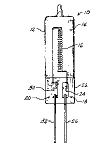
FIG. 2 shows a perspective cross-section and cutaway view of an
15 exemplary distributed feedback semiconductor laser for use as DFB laser 12 inlightwave system 10 in accordance with the principles of the invention. The DFB
laser shown in FIG. 2 is a buried heterostructure having a reversed-bias p-n blocking
region. Other structures such as buried ridge, crescent or V-groove, double channel
planar buried heterostructure, semi-insulating blocking region planar buried
20 heterostructuIe and the like are contemplated for use as embodiments of DFB laser
12.
Semiconductor structures such as the one shown in FIG. 2 are grown
using epitaxial growth techniques such as liquid phase epitaxy, molecular beam
epitaxy, chemical beam epitaxy and vapor phase epitaxy. These techniques are
25 described in the literature and are well known to those sldlled in the art. See, for
example, H. C. Casey et al., Heteros~ucture ~ Vols. A and B, Academic Press
(1978). Also, see U. S. Patent 4,023,993 for a description of a method for making a
distributed feedback laser.
As sho vn in FIG. 2, the DFB laser includes an n-type Sn:InP
30 substrate 23 on which the reversed-bias p-n blocking region and the buried
heterostructure are grown. Contact layers 24 and 25 are shown as broad area
metallic contacts deposited on opposite sides of the DFB laser for biasing and
curTent injection. Standard ohmic contact fabricadon techniques such as multi-layer
evaporation of metal films, alloy evaporation, sputtering and annealing may be
35 employed to realize the ohmic contacts for the particular DFB laser. In the laser
shown in FIG. 2, contact 24 is a standard Au-Zn contact whereas contact 25 is an
~ .
2C)()~)12
evaporated Au-Ge-Ni contact.
Using standard epitaxial growth techniques, a heterostructure is grown
on substrate 23 in the following order: an addidonal n-type Sn:lnP buffer layer (not
shown) approximately 511m thick; an undoped quaternary (InxGal xAsyPl y) active
5 layer 26 approximately O. l S ~m thick and having suitable mole fracdons x and y to
produce a characterisdc wavelength ~p substandally at the peak of the gain profile
curve as desired --- in this example, the characteristic wavelength is selected to be
approximately l.Sl ~m; a p-type guide layer 27 comprising Zn:InxGal xAsyPl y
approximately O.lS llm thick and having suitable mole fracdons x, y for
10 approximately 1.3 ~m; a p-type Zn:InP cladding layer 28 approximately 3 ~,lm thick;
and p-type quaternary cap layer 29 approximately 0.7 llm thick. Standard stripe
masking using photolithography and etching techniques (for example, bromine
methanol etch) are employed to produce the heterostructure mesa.
After the heterostructure mesa is formed, successive growth steps for p-
15 blocking layer 22 and n-blocking layer 21 are performed over the substrate 25.
Blocking layer 22 comprises Zn:InP approximately 0.5 llm thick and blocking
layer 21 comprises Sn:InP to a thickness sufficient ~o substandally planarize the
endre semiconductor structure for contacdng.
It is understood that dopant concentradons of approximately lOl7 to
20 lOl8 cm~3 are suitable for the Sn and Zn dopants in the layers of the DFB laser
described above. After &al preparadon, the laser is cleaved to produce at least two
end facets in planes perpendicular to a directdon of light propagatdon supported in the
heterostructure. Since the laser shown has a corrugadon grating as the integrated
feedback structure between the facets, it is generally acceptable practice to apply
25 and-reflecdon coatings to the at least two end facets to reduce end facet reflections to
a minimurn.
Also shown in FIGS. 2 and 3, the integrated feedback structure of the
DFB laser includes a corrugadon gradng 3l which is formed in guide layer 27 on the
side opposite the interface with acdve layer 26. Shape, depth and pitch or period of
30 the gradng are variable and depend on the gratdng placement together with the result
desired therefrom.
In principle, the integrated feedback structure of the DFB laser includes
spadally periodic perturbadons in the transmission characterisdcs of the laser
waveguide formed substandally condnuously along the direcdon of lightwave
35 propagadon in the laser waveguide and substandally transverse to the propagation
direcdon of optical energy in the waveguide. Spadally periodic perturbatdons of the
200Gl~
- 8 -
transmission characterisdc of the waveguide may take the form of variadons in gain,
index of refracdon, propagadon constant, or other parameter of the waveguide
medium for the laser.
In accordance with the principles of this invention, the period of the
S gradng effecdve over the guiding region of the laser is given as an effective period,
~eff > ~pM/2n, where ~p is the characteristdc wavelength substantially at the gain
peak or gain maximum for the semiconductor structure, M is the order of the grating
expressed as an integer greater than or equal to one, and n is the modal or effective
index of refractdors for the waveguide mode of the semiconductor laser. It is
10 contemplated that, while transverse positioning of the gratdng lines is desired, an
, angular displacement (twist) of the grating lines may occur so that the grating lines
lie substantially transverse to the direcdon of lightwave propagation for the DFB
laser.
It is contemplated that first (M=1) or higher order (M=2,3,...) integrated
15 feedback structures such as corrugation gradngs may be udlized. Such gradngs may
be fabricated using standard electron beam, photolithographic and/or holographicpatterning techniques with the necessary subsequent wet or dry etching steps. The
gradng shape may be sinusoidal as shown in FIGs. 2 and 3 or triangular, rectangular,
trapezoidal, semi-circular or some other known complex functdon. For various
20 gradng profiles and fabricadon techniques, see Elect. ~ ~ Vol. 19, No. 25/26, pp.
107~7 (1983).
Positior~ing of the grating with respect to the actiYe layer can be varied
so that the grating rnay be on the substrate below the acdve layer, or on the active
layer, or on sorne other layer near the active layer. Of course, grating coupling
25 strength must be considered when selecting a grating position because the grating
coupling strength is determined by the grating position vis-a-vis the waveguide
mode, the gradng or corrugadon depth measured from peak to trough, and the
difference between refracdve indices for the materials bounding the corrugation or
grating.
As one addidonal modification of the gradng structure, it is well known
that ~J4 shift regions may be included within the gradng. These ~J4 shift regions are
known to provide additional frequency stability for the DFB laser. One exemplary
~/4 shift is shown as region 30 in FIG. 3. Such regions need not be centrally located
in the gradng structure. Other types of shift regions are contemplated for use herein
35 such as step-index of refracdon changes in a guide layer or a linearly increasing
thickness of a guiding layer or the like as disclosed in U. S. Patents 4,096,446,
20061~
.9
4,648,096, 4,665,528, 4,701,930.
In the exemplary embodiment shown in F~Gs. 2 and 3, a first order grating i5
shown with an effective period ~,lr which satisfies the criterion described above for
5 detuning the grating to be at a wavelength which is longer than the gain peak or gain
maximum wavelength as described above mathemat;cally. The corrugation grating shown
in the FIGs. has a pitch of approximately 2384 A and a depth of approximately 800
This grating was chosen to achieve detuning of approximately 400 ~ from a gain peak
wavelength of approximately 1.51 ~Lm (lp) to an operating wavelength of 1.55 ,um (1B)-
In order to accomplish this detuning, it is necessary to select the amount of
wavelength detuning desired. Using standard calculation techniques which are well known
to those skilled in the art, the modal index of refraction of the laser seructure is
determined using the compositions and layer dimensions for the DFB laser. Index values
are obtained from IEEE J of Quant. Elect.. QE-21, pp. 1887 et seq. (1985~.
Detuning the grating period to be such that the Bragg wavelength is longer than
the wavelength of the gain peak for the semiconductor material causes the resulting DFB
laser to have an unusually large linewidth enhancement factor, ~. For general discussion
of measurement of the linewidth enhancement factor, see the following articles: IEEE J.
of Quant. Elect.~ QE-18, pp. 259 et seq. (1982); Appl. Phvs. Lett.. 42(8), pp. 631 et seq.
(1983); Elect. Lett.~ 23, pp. 393-4 (1987); Elect. Lett.. 22, pp. 580-1 (1986). As a result of
proper detuning in accordance with the principles of the invention, the resulting DFB
laser provides a large carrier-mediated FM response for reducing current drive
requirements and also for flattening the F~ response to be substantially uniform.
FIG. 4 shows a combined plot of linewidth enhancement factor versus wavelength
(curves 42 and 43) and gain versus wavelength (curve 41). The active layer was designed
to be quaternary m-v semiconductor material, LnGaAsP, with mole fractions x=0.74 and
y=0.6 so that Ap is slightly less than 1.3 ~m. The linewidth enhancement factor is shown
to increase with increasing wavelength for a buried heterostructure DFB laser in curve 42
and a multiple quantum well DFB laser in curve 43. That is, each DFB laser exhibits
more chirp with increasing wavelength. Shaded region 44 depicts those wavelengths to
which the integrated feedback stNcture such as a Bragg grating may be tuned for the
DFB laser so that
A
- 10-
the operadng wavelength of the laser (~B) iS greater than the gain peak wavelength
for achieving large linewidth enhancement and excellent direct current frequencymoduladon operadon.
In another example from experimental pracdce, a DFB laser having a
S properly designed gradng and waveguide structure was frequency modulated directly
using NRZ data sequences with a peak-to-peak current drive of 4 mA. The residualintensity moduladon was less than 7% and there was no apparent degradadon due tononuniform FM response which indicates that the invendve laser structure
overcomes the problems of the prior art by substandally eliminadng nonuniform FMlO response. Degradadon, if any, would have been noticed because the pseudorandom
sequence has a length 223-l at a data rate of 2Gbps giving rise to spectral
components below 1 KHz which is well below the thermal cutoff frequency --- a
regime identified with classic nonuniform FM response.
It is understood that, while the material system InGaAsP/InP is
15 described above for fabricadng the distribused feedback laser, other materialcombinadons may be selected from other semiconductor Group m-v systems such
as GaAs/AlGaAs, InGaAs/InAlAs, InGaAs/InGaAlAs, GaAsSb/GaAlAsSb and
GaAs/AlAs. In these sen~conductor systems, the layers may be latdce-matched to
suitable GaAs or InP substrates. Mismatching is also contemplated wherein strained
20 layers are grown over the substrate materia1. Finally, extension of the device
structures is also contemplated to semiconductor compounds in Group II-VL
..