Note: Descriptions are shown in the official language in which they were submitted.
20~6~
VERY Tl-IIN EL~CTRICAL STEEL STRIP IIAVING LOW
CORE LOSS AND l-lIGH MAGMETIC F'LUX DENSITY AND
A PROCESS FOR PRODUCING TIIE SAME
TECHNICAL FIELD
This invention relates to a very thin elec-trical
steel strip in which the grains or crystals have a <OO1>
axis of easy magnetiza-tion lying in parallel to the
rolling direction oE the strip and the {110} plane of
crystal lattice lying in parallel to ~he strip surface,
i.e. a {110} <OO1> type of orienta-tion as designated by
Miller's Indices, and to a process for producing the same.
The strip of this invention has a high magnetic flux
density and a low core loss despite ;ts small thickness,
and is suitable Eor use in making high frequency power
source ~ransformers and control devices.
BACKGROUND ART
The basic concept on the magnetic properties of
~rain-oriented electrical steel shee-ts was studied for the
first time when the magnetic anisotropy of a single
crystal of iron was discovered in l9Z6 [K. Honda and S.
Kaya: Sci. Reps., Tohoku Imp. Univ., 15 (1926), p. 721].
It has become possible to produce grain-orien-ted
electrical steel strips having greatly improved magnetic
properties since a process for producing a material having
a {110} ~OO1> type of texture was invented by N.P. Goss
~United State~s Patent No. 1,965,559).
The aggregation of the grains hav:ing a ~110} <001>
type of orientation in electrical steel strips is achieved
by utilizing a ca-tas~rophic phenomenon of grain growth
called secondary recrystallization. The con-trol of
secondary recrystallization essentially requires the
control of a primary recrystallization texture and
structure prior to the secondary recrystallization -thereof
and the control of an inhibi-tor, i.e. a fine precipitate,
or an element of the intergranular segregation type. Th0
inhibitor inhibits the growth of any grains other than
those having a {110} <001> type of orientation in the
primary recrystallization texture and enables the
selective growth of the grains having a {110} <001> type
of orientation.
The following are the three typical processes
which are known for the industrial manu~acture of grain-
oriented electrical steel strips or sheets:
(1) The process as disclosed by M.F. Littmann in
U.S.Paten-t No.Z,599,340 (Japanese Patent
Publication No. 3651/1955) which employs ~wo steps
of cold rolling utilizing MnS as the lnhibitor;
(2) The process as disclosed by Taguchi and Sakakura
in U.S.Patent ~o.3,287,183 (Japanese Patent
Publication No. 15644/1965) which adopts a
reduction rate exceeding 80% in final cold rolling
utilizing an inhibi-tor comprising AlN and MnS; and
(3) The process as disclosed by Imanaka et al. in
9Z
U.S.Pa-tent No.3,932,234 (Japanese Pa-ten-t
Publication No. 13469/1976) which employs two
steps of cold rolling u-tiliz;ng an inhibitor
comprising MnS (or MnSe) and Sb.
These processes have made it possible to produce
on a commercial basis grain-oriented electrical steel
strips in which the grains having a {110) <001~ type of
orienta-tion have so hi~h a degree of sharpness tha-t the
strips have a magnetic flux densi-ty (B8 value) of about
1.92 tesla. With a reduction of sheet thickness, however,
the inhibitor exhibits a sensitive behavior of change
through the interface which makes it difficult to produce
thin grain-oriented electrical steel strips on an
industrial basis. The main strips which are industrially
available have, therefore, a thickness which is not
smaller than 0.20 mm.
The core loss of grain-oriented electrical steel
strips in a high frequency range increases in proportion
to the square of their thickness, as reported by, for
examplQ, R.H. Pry and C.P. ~ean in J. Appl. Phys., 29
~1958~, p. 532. Therefore, it is essential to make a
strip having a small thickness if it is desirable to
obtain a sheet having a low core loss.
In 1949, M.F. Littmann disclosed a process for
producing very thin silicon steel strip ;n United States
Patent No. 2,473,156. This process comprises cold rolling
a starting ma-terial having a (110} <001> type of crystal
~U~362~3~
or:lentation atlcl subjectirlg it to a recrystallizing
treatment, and does not use any inhibitor. The products
of the process had a thickness of 1 -to 5 mils (25.4 to 12
microns), a maynetic flux clensity (B8 value) of 1.600 to
1.815 teslas, ~nd a core loss of 0.26 to 0.53 W/lb. (0.44
to 0.90 W/kg) at a frequency of 60 Hz and a maximum
magnetic flux density of 1.0 T. This process is still
used for producing very thin electrical s-teel strip.
DISCLOSURE OF THE INVENTION
As a result of the remarkable development of
electronic apparatus, there has recently grown a demand
for smaller and more efficien-t high-frequency power source
transformers and control devices. The conventionally
available very thin electrical steel strip, however, has a
low magnetic flux density, as hereinabove stated, which is
so low as not to permit the selection of a suEficiently
high design value of magnetic flux density to attain a
satisfactory reduction in si~e of apparatus. Moreover, it
has a very high core loss particularly in a high
excitation range.
The inventors of this invention have found that it
is essential for a very thin electrical steel strip having
a low core loss, particularly in a high excitation range,
to consist of a ma-terial having a silicon content not
exceeding 8%, the balance thereof substan-tially being
iron, and an average grain diameter not exceeding 1.0 mm,
and to have a thickness not exceeding 150 microns and a
B8/BS ~magnetic flu~ density/satura-tion magnetic flux
density) value which is larger than 0.9, ancl hereby
propose the electrical s-teel strip sa-tisfyiny those
requirements and a process for producing it, which will
hereinafter be clescribed in detail,
Ref~rring to the machanism of magne-tization which
governs the core loss of an electrical material, it has
hitherto been usual to consider the degree of sharpnass in
the crystal orienta-tion of the material as an unimpor-tan~
factor in a high frequency range, but to consider it more
important to -taks another method, such as increasing the
amount of silicon to raise the resistivity of the
material, as is obvious from the following statement:
"Although the movement of the magnetic domain
walls plays a principal role in the process of
static or low frequency magnetization, it is
considered better in a high frequency range to
achieve magnetization by domain ro-tation, since in
a high frequency range, the domain walls are not
only difficult to move, but also the movement
thereof produces a loss of energy"
[Chikazumi: Applied Physics, 53 ~1984), p. 294].
According to, for example, Y. Takada et al. who compare
qrain-oriented and non-oriented electrical steel strips
and 6.5% Si-Fe in J. Appl Phys , 64 ~1988), pages 5367 to
5369, the grain-orien-ted electrical s-teel s-trip having a
controlled crys-tal orienta-tion shows the lowest core loss
Z~3~
at a frequency of 50 }Iz, but at a frequency of 10 kHz,
6.5%Si-Fe shows the lowest core loss and the grain-
orien-ted and non-oriented electrical steel strips having a
substantially equal silicon content do no-t show any
appreciable difference in core loss from each o-ther, and
it is, therefore, ovbious that the crystal orientation
does not have any subs-tantial effect on core loss in a
high frequency range (see Table 1).
Table 1
Thickness B8 Core loss ~/kg)
(mm) (T) 10/50 2/lOk
Grain-oriented 0.3 1.93 0.35~150
electrical steel
strip ~3.2% Si~
Non~oriented 0.5 1.42 1.36180
electrical steel
strip (3.0% Si)
6.5%Si-Fe 0.3 1.27 0.4974
" 0.5 1.27 0.58106
As a result of our research on very thin
elec-trical s-teel s-trip used for making high-frequency
power source transformers, control devices, etc., we, the
inventors of this invention, have found that a very thin
electrical steel strip having a thickness not exceeding
150 microns, an average grain diameter not exceeding 1.0
9Z
mm, and a magnetic flu~ density B8/Bs value wllich is
larger than 0.9 has a remarkably low core loss in a high
frequency range.
Figure l(a) sllows the relation between magnetic
flux density and core loss which is measured at 1.5 T
and 1000 Hz. It is obvious therefrom that the strip having
a B~ value which is equal to, or greater than, 1.85 teslas
(B8/B9>0.9) ha~ a low core loss in a high frequency range.
Figure l(b) shows ~he relationship between core loss and
frequency of very thin electrical steel sheets of this
invention having a magnetic flux density or B8 value of
1.94 T, which are shown by white circles, and that of
conventional products having a B8 value of 1.60 T, which
are shown by black circles. It is obvious from it tha-t a
very thin electrical steel strip having a high magnetic
flux density shows a low core loss in a high frequency
range. A very thin electrical steel strip having a high
magnetic flux densi-ty not only has a low core loss, but
also allows for the choice of a high design value of
magnetic flux densi-ty which enables a reduction in size of
apparatus and a drastic improvement in characteristics of
high-frequency power source transformers or control
devices.
As a result of our research, we have discovered
that a very thin elec-trical steel strip containing not
more than 8.0% by weigh-t of silicon and 0.005 to 0.30% by
weigh-t of Sn or Sb, or both, the balance thereof
substan-tially being iron, and having a thickness not
exceeding 150 microns, an av~rage grain diame-ter not
exceeding 1.0 mm and a magnetic flux density B8/BS value
which is larger than 0.9 shows a very low core loss in a
lligh frequency range.
Descrip-tion will now be made of a process for
producing such a very thin electrical steel strip.
We considered that a reduction in thickness of an
electrical steel strip would make it difficult to control
an inhibi-tor and achieve s-table secondary recr~stal-
lization, as hereinbefore stated, and studied the
possibility of attaining a high degree of sharpness of
grains having a ~110} <001~ type of orientation by primary
recrystallization not employing any inhibitor. As a
result, we have found that lt is possible ~to produce a
very thin electrical steel strip having an aggregation of
grains having a sharp {110~ <001> type of orientation, and
a low core loss by employing a starting material
comprising grain-oriented electrical steel having a very
high degree of sharpness of grains having a {110} <001~
type of orientation, cold rolling it to a final thickness
not exceeding 150 microns, and subjecting it to primary
recrystallization annealing, while inhibiting
recrystallization from the grain boundary.
We have found it from the following experiment.
We used as a starting material a grain-oriented electrical
steel strip containing 3.3% Si, 0.002% C, O.OOZ% N, 0.002%
Al, 0.0002% S and 0.13% Mn, all by weight, the balance
thereof substantially being iron, and having a texture of
grains having a ~110} <001> type of orienta-tion, a
magnetic flu7~ density (B8 value) of 1.92 T, an average
grain diameter of 40 mm and A -thickness of 0.30 mm. We
cold rolled it to a final thickness of 0.09 mm (90
microns) and annealed it at 850~C for 10 minutes ~o
complete its primary recrystallization.
Figure 2 shows the texture of the product obtained
from the experiment. As is obvious therefrom, -the grains
of primary recrystalliza-tion include not only ones having
a ~110} <001> type of orientation, but also ones having a
{111} <011> type of orienta-tion, and an increase of the
latter type of grains brings about a lowering of magnetic
flux density.
The texture is definitely different from that
ob-tained by -the process disclosed by Li-ttmann in United
States Patent No. 2,473,156, which has a {210} <001> to
{310} <001> type of orientation. This is apparently due
to the fact that the starting material employed by
Littmann had a magnetic flux densi-ty or B1o value which
was as low as 1,~4 T, and a poor orientation of the {110}
<001> type. It, therefore, follows that -the manufacture
of a product having a high magnetic flux density requires
the use of a starting material having a high degree of
orientation of the {110} <001> type and the inhibition of
primary recrystallization of grains having a ~111} cO11>
Z~
type of orientation. ~s a result of our research on the
cold rolling and recrystallization of the starting
material, we have found that the grains having a {110}
<OO1> type of orienta-tion nucleate and grow in the grains
of the starting material, while the grains having a ~111}
<O11> type of orien-tation nucleate grow from the grain
boundary (See Figures lO(a) and lO(b~).
This discovery teaches that it is possible to
obtain a very thin product having a high degree of
orien-tation of the ~110} <OO1~ type by employing a
starting material having a small grain boundary area, or
lnhibiting the occurrence o~ nuclei from the grain
boundary.
BRIEF DESCRIPTION OF T~IE DRA~:[NGS
Figure l(a) is a graph showing the magnetic flux
densities and core losses of very thin electrical steel
strips produced by various processes;
Figure l(b) is a graph showing the core losses of
very thin electrical steel strips having different
magnetic flux densities in relation to frequency;
Figure 2 is a pole figure showing the texture of
the product obtained from the experiment from which the
discovery on which this invention is based was made;
Figure 3 is a graph showing the magnetic ilux
densities (B8 values) of very thin electrical steel strips
of this invention containing Sn in relation to their Sn
contents;
-- 10 --
E'igure 4 is a graph showing the magne-tic flux
densities of strips of this invention containing Sn and
not containing Sn in relation to the ratios of cold
reduc-tion;
Figure 5 is a graph showing the magnetic flux
densities of the products obtained from the experiment as
hereinabove described, in relation to the temperature and
time as employed for primary recrystallization annealing;
Figure 6 is a graph showing the magnetic flux
densities o~ strips havillg different cold reduction ratios
and final thicknesses in rela-tion to the heating rate as
employed for primary recrystallization annealing;
Figure 7 is a graph showing the magnetic flux
densities (B8 values) of products of this invention and
conventional products in relation to their thicknesses;
Figure ~(a) is a graph showing the core losses of
products of this invention as compared with the
conventional products at 1000 ~Iz in relation to exciting
flux density;
Figure 8(b) is a graph showing -the core losses of
products of this invention as compared with the
conventional proclucts a-t 400 Hz in rela-tion to exciting
flux density;
Figure 9(a) and 9(b~ show the grain structure of
the materials according to Example 2 of this invention as
annealed at 800~C and 1000~C, respectively; and
Figures lO(a) and lO(b) are a photograph showing
Y~ 3~
the orientation of primary recrystallization grains formed
in the vicini ty of the grain boundary of the star-ting
na-terial which were revealed by etch pits, and a model
diagr~m prepared from the photograph, respectively.
BEST MODE OF C~RRYING OUT THE INVENTION
The invention will now be described in further
detail with reference to specific steps of a process for
producing a very thill electrical steel strip.
Based on our discovery of the fact that it would
be important -to use a startiny material having a high
degree of orientation of the {110} <001~ type and reduce
the occurrence of nuclei from the grain boundary in order
to obtain a product having a high magnetic flux density,
we, the inventors of this invention, attempted to produce
very thin electrical steel s-trips by employing as starting
materials grain-oriented electrical steel sheets having
different grain diameters and B8~BS values which were
greater than 0.9, cold rolling -them at reduction ratios of
60 to 80~ to final thicknesses not exceeding 150 microns,
and annealing the cold rolled products at temperatures of
100~ to 900~C for primary recrystallization. We
determined the magnetic properties of the strips, and
found that it would be necessary to use as a starting
material a grain-oriented electrical steel strip having a
grain diameter RD of at least 20 mm in the rolling
directlon in order to obtain a very thin electrical steel
strip having a magnetic flu~ density of at least 1.85
- 12 -
2~2~
teslas. We also found -that the grain diame-ter RC of the
5 tarting material in -the direction perpendicular to the
rolllng direc-tion was a s-till more important Eactor and
had to be at least 40 mm. We proposed a method for the
ind~strial production of starting materials satisfying
tho~e requirements in, for example, Japanese Patent
Application laid open under No. 215419/1984.
We also studied the possibility of inhibitlng the
occurrence of nuclei forming badly oriented grains, from
the grain boundary and found tha-t the addition of one or
both of Sn and Sb to a grain-oriented electrical steel
strip used as the starting material would make it possible
to inhibit the occurrence from the grain boundary of
nuclei forming grains having a {111} ~011> type of
orientation and increase grains having a {110} <001> type
of orientation to thereby yield a product having an
improved magnetic flux density.
Our discovery was obtained from the following
experiment. We used grain-orien-ted electrical steel
strips containing 3.2% Si, 0.002% C, 0.001% N, 0.002% Al,
0.0004~ S, 0.05% Mn, and O to 0.5% of one or both of Sn
and Sb, all by weight, and having a magne-tic flux density
(s8 value) of 1.90 T, an average grain diameter of 5 to 40
mm and a thickness of 0.14 mm. We cold rolled them to a
final thickness of 30 microns and annealed the cold rolled
products at 350~C for 10 minutes to complete primary
recrystallization.
- - 13 -
.......
9~
Figure 3 shows the magnetlc flux densities of the
products in relation -to the tin conten-ts of the starting
materials. As is obvious therefrom, the addition of 0,01%
or more of Sn made it possible to inhibit the occurrence
of nuclei forming grains having a ~111} <011> type of
orientation from the grain boundary and thereby obtain a
product having an improved magnetic flux density. The
addition of over 0.30% of Sn, however, rèsulted in a
product having a low magnetic flux density. This may be
due to the fact that the starting material had so small
crystal grains and so large a grain boundary area that
more nuclei occurred from the grain boundary.
The starting material containing a total of 0.03
to 0.30% of one or both of Sn and Sb yielded a product
having a magnetic flux density (B8 value) which was as
high as 1,94 teslas, as shown in Figure 4. We also found
that when the starting material contains one or both of Sn
and Sb the best cold reduction ratio, at which the product
having the highest magne-tic flux densi-ty could be
manufactured, shifted to ~ligher reduction ratio. The
addition of Sn or Sb enabled the manufacture of a very
thin product without calling for the use of a starting
material having a smaller thickness. The addition of Sn
or Sb, or both, makes it possible -to produce very thin
electrical steel strips having different thicknesses from
starting materials having the same thickness, since a very
wide ranye of cold reduction ratios can be employed for
9;~
manufacturiZlg products having a high magne-tic flux densit~
from materials containing Sn or Sb, or both, as compared
witl-l the range which can be employed for the cold
reduc-tion of materials not containing Sn or Sb.
We also found that it was possible to cause the
selective forma-tion and growth of grains having a {110}
<001~ type of orientation when a cold rolled material was
held or gradually heated in a low temperature range before
its tempera-ture was raised -to complete primary
recrystalliza-tion.
C.G. Dunn reported in Acta. Met., 1 ~1953), page
163 that a product having a low magnetic flux density (as
determined by means of torque) had resulted from
preliminary low-temperature annealing a-t 550~C followed by
annealing at 980~C. We, however, made a detailed study of
the conditions for primary recrystallization annealin~,
and found that, though a long time of annealing a-t a low
temperature causes the formation and growth of grains
having a {111} <011> type of orientation, as well as ones
having a ~110} <001> type of orientation, and thereby
yields a product having a ~ow magnetic flu~ density, the
restriction of low-temperature annealing to a period of
time within which primary recrystallization is not
completed makes it possible to cause the forma-tion of only
grains having a {110} <001> type of orientation and obtain
a product having a high magne-tic Elux density if the
tempera-ture is thereaEter raised to cause the growth of
- 15 -
the gra;ns.
Reference is made to Figure 5 showing the magnetic
flux densities (B8 Values) of very thin electrical steel
strips in relation to the conditions of low-temperature
annealing which were employed for producing the strips.
The strips were produced from grain-oriented electrical
steel strips containing 3.3% Si, 0.002% C, 0.001% N,
0.002% Al, 0.002% S and 0.13% Mn, the balance thereof
substantially being iron, and having a magnetic flux
density (B8 value) of 1.92 T, an average grain diameter of
40 mm and a thickness of 0.1~ mm. The sheets were cold
rolled to a final thickness of 0.05 mm (50 microns), and
the cold rolled products were annealed at temperatures of
400~ to 700~C for one to 30 minutes, and at 850~C for 10
minutes to complete primary recrystallization. I-t is
obvious from Figure 5 that very thin electrical steel
strips having a high masnetic flux density can be produced
when low~temperature annealing is carried out at a
temperature T of 400~ to 700~ C for a period of time t
which is equal to, or longer than, 20 seconds, and is
shorter than (-6T(~C) ~ 4400) seconds, and is followed by
temperature elevation to complete primary
recrystallization.
Cold rolled strips of the same nature were
annealed by heating to 850~C at differen-t rates of 2.5 x
10 30C to 1.0 x 10²~C per second, and holding at 850~C ~or
10 minutes. Figure 6 shows the magnetic flux densities
- 16 -
(B8 Values) of the products in rela-tion to the heating
rate. As is ovbious therefrom, i~ is possible to make a
product having a high mayne-tic flux density as deEined in
accordance with this invention by a B8/BS ratio which is
~reater than 0.9, if the heating rate which is employed
for the annealing of a cold rolled produc-t lies within the
range of 5.0 x 10 ~C to 5.0 x 10 C per second. It will
be noted that these conditions turn out to be equal to the
temperature and time conditions shown in Figure 5.
The use of a starting material having a large
grain diameter and a high grain orienta-tion of the {110}
<001> type, the addition of one or both of Sn and Sb to
the starting material and the low-temperature annealing
performed for a certain length of time prior to the
completion of primary recrystallization make it possible
to inhiblt the formation and growth of grains having a
{111} <011> type of orientation from the grain boundary,
which results in the manufacture of a product having a low
~agnetic flux density, and achieve the selective formation
and growth of grains having a {110} <001> type of
orientation, as hereinabove stated. It is needless to say
that the process in which those fea-tures are incorporated
ensures the produc-tion of very thin electrical steel
strips having a s-till higher magnetic flux density.
Thus, this lnvention pr.ovides a very thin
electrical steel strip having a magnetic flux density
which is by far higher than that of any conventional
- 17 -
32
produc-t, as shown in Figure 7.
It is possible to use any grain-or~ented
electrical s-teel strip having a texture of -the {11~} <001
type as the starting ma-terial for the strip of this
invention, irrespective of the process which is employed
for making the strip. It is possible to use, for example,
a grain-oriented electrical steel strip as produced by any
of the processes disclosed in Japanese Patent Publications
Nos. 3651/1955, 15644/1965 and 13469/ 1976 and still used
on an industrial basis, as hereinbefore stated, or one
produced by cold rolling and annealing a rapidly cooled
strip of 4.5~Si-Fe steel as disclosed by Arai et al. in
Met. Trans., A17 (1986), page 1295. The s-tarting material
for the strip oE this inven-tion may have a silicon content
not exceeding 8%. A material having a silicon content
exceeding 8% has a saturation magne-tic flux density of 1.7
T or below which makes it unsuitable as a magnetic
material, and is also likely to crack when it is cold
rolled. A ma-terial having a silicon conten-t of 2 to 4% is
preferred, as it has a saturation magnetic flux density
which is as high as at least 1.95 T, and a high degree of
cold workability. The material may contain impurities,
such as Mn, Al, Cr, Ni, Cu, W and Co.
The starting material is cold rolled after its
glass film is removed, and the cold rolled material is
annealed Eor primary recrystallization in an atmosphere
having a composition ancl a dew point which do not cause
- 18 ~
92
any o~idation of iron. The a-tmosphere may consist of an
inert gas such as nitrogen, argon etc., or hydrogen, or a
mixture of an iner-t gas and hydrogen. Then, an insulating
film as disclosed in, for example, Japanese Patent
Publicatlon No. 283~5/1978 is formed on a very thin
electrical steel s-trip.
E~AMPLES
Example 1
Grain-oriented electrical steel strips containing
3.3% Si, 0.1% Mn, 0.001% C, 0.00~% N, 0.002% Al and 0.001%
S, the balance -thereof substantially being iron, and
having a B8 value of 1.98 T, a grain diame-ter RD ~~ 45 mm,
a grain diame-ter RC of 500 mm and a thickness of 170
microns, which is produced by the method disclosed in
Japanese Patent Application laid open under No.
215~19/1984, were pickled for the removal of glass films,
and were cold rolled to a final thickness of 50 microns.
Then, they were annealed at 800~C for two minutes in a
hydrogen atmosphere, followed by annealing in a nitrogen
atmosphere for the formation of insulating films.
The products were sub~ected to magnetic domain
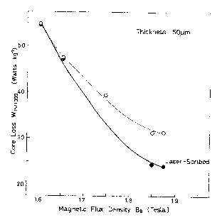
refining treatment by laser scribing. Figures B(a) and
8(b) show the magnetic properties of the products as
annealed and as laser scribed at the frequencies of 1000
Hz and ~00 Hz, respec-tively. As is obvious therefrom, the
products of this inven-tion showed by far lower core losses
than the conventional produc-ts. A-t the frequency of 400
- 19 -
92
Hz and a magnetic flux density of 1.5 T, for example, the
product of this inven~ion showed a core loss of 11 W/kg
and the laser-scribed product thereof showed a core loss
of on.ly ~ W/kg, while the conventional product showed a
core loss oE 15 W/kg.
It is particularly to be noted that there has
~ hitherto not been available any data showing the core loss
of any similar product at an exciting flux density which
is as high as 1.~ T. The product of this invention can be
used in such a high excita-tion range showing a very low
core loss.
~xample 2
The same cold-rolled strips as obtained in Example
1 were annealed at 800~C for two minu-tes and then at
1200~C for 10 hours in a hydrogen atmosphere. Then, the
insulating film forming and magnetic domain refining
treatments of Example 1 were repeated, and the magnetic
properties of -the products were examined. The results
were as shown below:
,
- 20 -
9;;~:
W15/400 : 6.5 W/kg
W1~/400 : 8.5 W/kg
W19/400 : 12.5 W/kg
W15/lOOO 20 W/kg
W17/lOOO 27 W/kg
Figures 9(a) and 9(b) show the textures of the
materials as annealed at 800~C and 1200~C, respec-tively.
The material as annealed at 800~C had an average grain
diameter of about 50 microns, and the ma-terial as fur-ther
annealed at 1200~C had its average grain diameter grown to
neariy 100 microns.
Example 3
A grain-oriented electrical steel strip containing
3.0% Si, 0.06% Mn, 0.003% C, 0.002% N, 0.001% Al, 0.001% S
and 0.07% Sn, the balance thereoE substantially being
iron, and having a B8 value of 1.88 T, a grain diameter RD
of 5 mm, a grain diameter RC of 3 mm and a thickness of
230 niicrons was pickled for the removal of a glass film,
and was cold rolled to a final ~hickness of 50 microns.
Then, it was annealed at 350~C for 10 minutes in an
atmosphere comprising 25% N2 and 75% H2 The product had
a magnetic flux density or B8 value of 1.91 T.
Example 4
Two kinds of grain-oriented electrical steel
strips containing 3.0 to 3.3% Si, having tin (Sn) contents
of 0.00% and 0.06%, respectively, and having a magnetic
- 21 -
flux density (B8 value) of 1.90 to 1 92 T were employed as
the starting ma-terials. One half of the starting
ma-terials had an average grain diame-ter of 2 to 20 mm,
while the other half had an average grain diameter of 40
to 60 mm. They were cold rolled at a reduction ratio of
~5% to a thlckness of 50 microns. Then, they were
annealed at ~50~C for 10 minutes in a hydroyen atmosphere.
The magnetic properties of the products are shown in Table
2.
Table 2
Sn content Average grain Magne-tic flux Remarks
(%) diameter (mm) density (T)
0.002 to 20 1.78 Comparative
0.0040 to 60 1.91 Invention
0.062 to 20 1.91 "
0.0640 to 60 1.93 "
Example 5
Two kinds of graln-oriented electrical steel
strips containing 3.0 to 3.3% Si, having tin (Sn) contents
of 0.00% and 0.06%, respectively, and having a magnetic
flux density (B8 value) of 1.90 to 1.92 T were empioyed as
the starting materials. One half of the starting
materials had an average grain diameter of 2 to 20 mm,
while the other half had an average grain diameter of 40
to 60 mm. They were cold rolled at a reduction ratio of
- 22 -
~3¢~
75% to a final thickness of 50 microns. Then, -they were
annealed in a hydrogen atmosphere at 500~C for five
minutes ancl then at 90U~C for 10 minutes -to comple-te
primary recrystallization. The magnetic properties of the
products are shown in Table 3.
Table 3
Sn con-tent Average grain Magnetic flux Remarlcs
(%) diameter (mm) density (T)
0.002 -to 20 1.88 Invention
0.0040 to 60 1.93 "
0.062 to 20 1.9~ "
0.0640 to 60 1.95 "
Example 6
A grain-oriented electrical steel strip con-taining
0.1% Mn, 0.002% C, 0.002% N, 0.01% Al and 0.002% S, the
balance thereof subs-tan~ially being iron, and having a B8
value of 2.01 T, a grain diameter RD of 12 mm, a grain
diameter RC of 8 mm and a thickness of 500 microns was
used as a starting material. It was a product by the
process disclosed in Japanese Patent Application No.
8ZZ36/1989 filed in the name oE the assignee of this
invention. It was pickled for the removal of a glass
film, and was cold rolled to a final -thickness of 150
microns. Then, i-t was annealed in a hydrogen atmosphere
at 550~C for five millutes and then at 850~C for 10 minutes
- 23 -
29~:
to complete primary recrystalliza-tion. The product had a
magnetic flux density (B~ value) of 1.99 T.
Example ~
A grain-oriented elec-trical steel strip containing
3.2% Si, 0.05% Mn, 0.002% C, 0.001% N, 0.002% Al, 0.001% S
and 0.02% Sb, the balance thereof substantially being
iron, and having a B8 value of 1.89 T, a grain diame~er RD
of 6 mm, a grain diameter RC of 6 mm and a thickness of
280 microns was pickled for the removal of a glass film,
and was cold rolled to a final thickness of 60 microns.
Then, it was annealed at 800~C for five minutes in an
atmosphere consis-ting solely of hydrogen. The product had
a magnetic flux density (B8 value) of 1.89 T.
INDUSTRIAL UTILITY
The product of this invention has the following
advantages:
~ 1) If it contains e.g. 3% Si, it has a magnetic flux
density at an exciting force of 800 A~M of 1.84 to 1.95 T
which is higher than that of the conven-tional product by
as much as about 0.2 to 0.4 T; and
(2) It has a very low core loss. For example, its
W15/400 value ls only about 50% of the core loss of the
conventional product. Moreover, it has a low core loss
not known in the past even in a high excita-tion range
exceeding 1.5 T.
The product of this invention, therefore, has a
high degree of utility in the realiza-tion of smaller and
- 24 -
more efflcient transEormers, par-ticularly high Erequency
power source transformers. It also prov.ides a great deal
of benefit when applied to control devices.
- 25 -