Note: Descriptions are shown in the official language in which they were submitted.
2006367 P 38 43 564.0
METHOD OF TESTING CONNECTING AND/OR SWITCHING
DEVICES AND/OR LINES
'rhe invention relates to a method of the type mentioned $n
the preamble of patent claim 1.
It is known to use, generate and transmit parity and check
bits or, in general, check words for error detection and error
correction and to draw conclusions from their syndrome, e.g., at
the end of a transmission channel, as to whether the signals were
transmitted in an error-free manner.
This also applies analogously for the transmission of
electric signals by means of switching system and networks, such
as e.g., by means of an optical section or by means of a space-
division multiplex switching matrix. In order to determine a
check word from a specific number of consecutive bits that form a
slgnal and, if applicable, to draw conclusions concerning the
presence of errors in the transmission channel by evaluation of
the received bits, there is a variety of methods that are known
as the theory of error detection and correction.
In corrections methods of this type, a certain time is
always required until a number of bits forming the unit to be
checked has been transmitted. Only when all of these bits have
been received is it possible to determine the syndrome from them
and to draw conclusions therefrom. If several channels are
involved in a transmission system, it may be necessary to use a
method of this type for each of these channels. This requires a
--1--
H. J. Matt et al 10-1-1
72430-107
relatively high switching effort. In addition, these methods
cannot be used if the signals on a line are not always traveling
in the same direction, for example, ln the case of bus lines.
It i~ the task of the present invention to develop a
method of the above-mentioned type further in such a way that the
switching effort is reduced and the capacity of the test procedure
i8 improved, in the sen~e that, at all times, not only the
information to be transmitted but also the complete utterability
of a system is checked. The method is particularly suitable for a
space-division multiplex switching matrix.
The present invention may be summarized according to one
broad aspect as a method for testing a spec-divislon multiplex
swltching matrix in which one or more of a plurality of input
llnes are connectable wlth one or more of a plurality of output
llnes sald testing being performed by mean~ of check words, said
method comprising the steps of. contlnuously derlvlng from slgnals
on the lnput llnes a first check word on a parallel basls ln
accordance wlth a set of rules; continuously deriving from signals
on the output lines a second check word on a parallel basis in
accordance with the set of rules; comparing the two check words;
and providlng an error indicatlon when the two check words
disagree.
According to another broad aspect the present inventlon
provldes a method of testlng connectlons between a first group of
lines and a second group of lines by means of check words,
comprising the steps of, continuously deriving from signals on the
llnes of the first group on a parallel basis a first check word
72430-107
accordlng to a set of rules; derlving from signals on the lines of
the Isecond group of lines on a parallel basis a second check word
ln accordance with the set of rules; derivlng an auxiliary check
word ln a parlty correction devlce whlch compensates for a second
check word when the second check word differs from the first check
word because one of the lines of the first group is connected to
other than a single line of the second group; and comparlng the
two check words and providing an error indication when the check
words disagree.
According to yet another broad aspect, the present
invention provides a method for testing connections between a
flrst group of lines and a second group of lines by means of check
word~, comprlslng the steps of- continuously derlving from signals
on the lines of the first group on a parallel basis, a first check
word in accordance wlth a set of rules, said first check word
consisting of a nu~ber which indicates how many llnes of the flrst
group are carrying a given signal simultaneously; deriving from
signals on the lines of the second group on a parallel basis a
second check word in accordance with the set of rules, sald second
check word conslsting of a number which indicate how many lines of
the second group are carrying a given signal slmultaneously; and
comparing the two check words and providing an error indication
when the check words disagree.
According to the invention, a check word, i.e., in the
simplest case, a parity bit is not derived from characters
transmitted or received consecutively in time on one channel, but,
instead, the check word is formed at each time from the plurality
72430-107
of signals present precisely at that time on a plurality of
channels or line~, and at the points of the system (for example,
lnput and output~ to be compared to each other. The transmltted
check word is compared to the check word formed at the output of
the system (syndrome check). If the two check words disagree,
i.e., if the syndrome is odd, then an error is present. Whereas,
in the known methods, the check words are, in
2b
~l
Z006367 P 38 43 564.0
each case, formed serially with respect to time and individually
with respect to channel, in the invention they are formed on a
parallel basis with respect to time and a comprehensive basis
with r,espect to system, i.e., not individually with respect to
channel.
The check word at the input is, of course,--if correctly
transmitted--identical to the check word at the output only if
every input signal is also present again as an output signal,
e.g., in a space-division multiplex switching matrix, if the
association of each input to each corresponding output is 1:1.
If the association of an input with a correspondingU~is not 1:1,
that is, if, for example, an input is connected to several
outputs (e.g., if a television program is received by several
subscribers) then this is taken into consideration, according to
the invention, by means of an auxiliary check word.
~ y means of the method according to the invention it is
pos8ible not only to check the lines and connections of a space-
division multiplex switching matrix but also, quite generally, to
check all systems, insofar as it is possible to associate, with
every check word derived from a first set of signals at a given
time, a check word derived from a second set of signals, so that
a comparison of the check words--possibly with a consideration of
system-related corrections--makes it possible to determine that
all channels and switching devices are operating perfectly.
Under these assumptions, the method according to the invention
H. J. Matt et al 10-1-1
Z006367 P 38 43 564.0
can also be used simultaneously on various hierarchical levels of
a system. The error detection can be combined with an error
eorrection in a known manner.
Exemplifying embodiments of the invention and its
ad-~antageous ~urther developments are described below with
re~erenee to the attached drawing, in which:
Figure 1 shows a spaee-division multiplex switching matrix K
aeeording to the state of the art.
Figure 2 shows the strueture of a switching cell S of Figure
1.
Figure 3 shows, as an exemplifying embodiment, a space-
division multiplex switching matrix similar to that in Figure 1,
with the inclusion of the invention.
Figure 4 shows, as an exemplifying embodiment, a eonnection
to a bu~ line with monitoring aeeording to the invention.
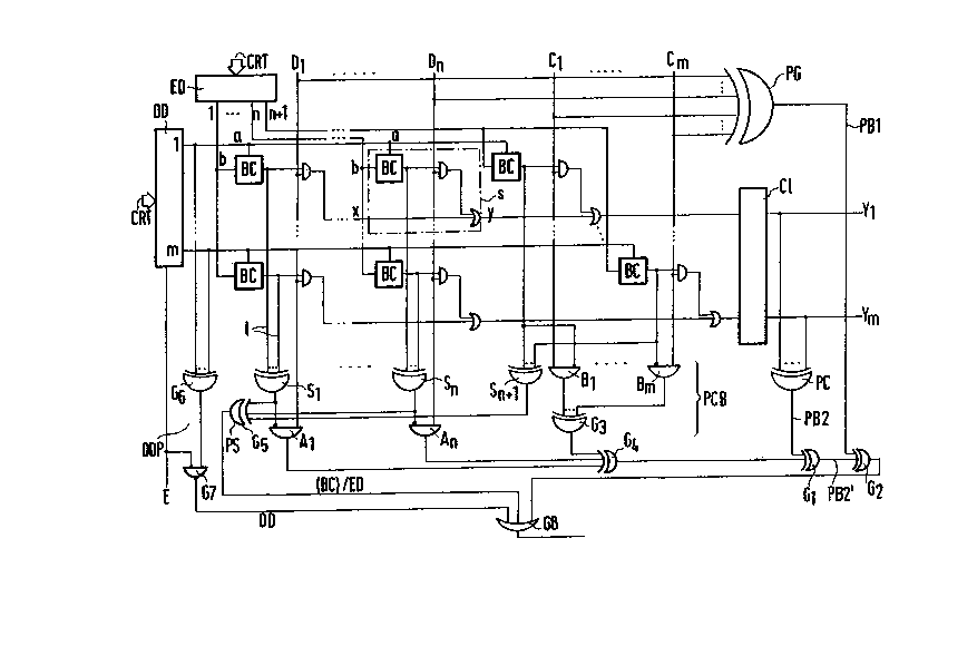
Figure 1 shows the known structure of a space-division
multiplex switehing matrix K, with (n + m) input lines and m
output lines as a ~(n + m) x m] switehing matrix. The (n + m)
input lines are divided into n input lines Dl, D2 . Dn and m
input lines Cl, C2 . . . Cm (expansion inputs). The m output
lines Yl, Y2 . . . Ym are also provided. Preferably, n = m =
16. At every point of interseetion of an input line Di with an
output line Yk, there is loeated a switching cell S with control
inputs a and b according to Figure 2. All eontrol inputs a of a
line are eonnected with the eontrol line of an output decoder OD
H. J. Matt et al 10-1-1
2006367 ~ 3a ~3 56~.0
associated with this line. All control inputs b of a column are
with the associated control line of an input decoder ED. In the
expansion input lines C, the diagonal association shown is
present. The control o~ the output decoder OD and of the input
decoder ED is carried out in a known manner and is indicated by a
bus CTR. The enabling of the output decoder OD is carried out by
means of a line E. A clocking circuit Cl is connected into the
output lines Yk.
If the inputs a and b of a switching cell S (Figure 2) are
in the 1 state, i.e., if a = b = 1, then Yk = Divxk, i.e~, an
output signal 1 appears on the output line Yk, if a 1 is present
either on the associated input line Di or on the input line xk
coming from the switching cell located ahead of it in the line.
This follows from the construction of the switching cell S with
use of conventional gates and of a bi-stable ~lip-flop according
to Flgure 2. The switching statc o~ thc ~witcl~ c~ll S 1~
determined by the st~te of the output Q of the flip-flop. It
forms a binary memory BC with the AND gates connected in series
and an inverter. Q becomes 1 when a = b = 1. If a = 1 and b =
O, then Q changes to O. If a = O, then Q remains unchanged.
Normally, the output decoder supplies 1 on one line and O on all
other lines, as soon as it has been enabled by means of E.
Otherwise, all lines a are equal to O. This results in the fact
that exactly one input line Di or Cj is switched to each output
line Yk.
-5-
H. J. Matt et al 10-1-1
:
Z006367 P 38 ~3 564.0
A space-driven multiplex switching matrix, with the
inclusion of checkers according to an exemplifying embodiment of
the invention, is shown in detail in Figure 3.
The data coming in on the input lines Dl, D2 . . . Dn and
the expansion input lines C1, C2 . . . Cm are applied--in
parallel~-to the application of the individual switching cells s--
to a parity generator PG, which derives a check word PBl (in the
example 1 check bit) therefrom. The derivation is carried out
according to general rules, i.e., approximately as shown in
Figure 3, such that a check bit "1" if the number of input lines
carrying the signal 1 is odd and is "0" if the number of input
lines carrying 1 is even. Other associations are, of course,
possible. The check bit PB1 is applied to an input of the XOR
gate G2.
The output lines Y1, . . ., Yn are applied to the parity
checker PC. In general, a check word, in this case, a check bit
PB2 according to Fiqure 3, ls derived in it and --this is
essential--this is done according to the same rules by which the
check bit PB1 has been derived in the parity generator PG, i.e.,
it is 1 if an odd number of input lines is carrying the 1, and it
is 0 if an even number of input lines is carrying the l. Under
the assumption that every input liné Di, Cj is connected with
exactly one output line Yk, the check words or check or parity
bits PBl and PB2 are identical (n + m > m).
--6--
H. J. Matt et al 10-1-1
Z006367
P 38 43 564.0
The check bit PB2 is applied to the first input of the XOR
gate ~1 If PB2 is equal to 1, then the output Gl also becomes
1, unless 1 is also applied to the other input of Gl (for
correction purposes). If PB1 and PB2 are both equal to 1, the
result is that this involves an exclusive OR gate, a signal 0 at
the output of G2 and therefore no ERROR alarm at the output of
the OR gate G8. In that case, the check was positive, i.e., it
had shown that their is no error between the input and output,
and therefore that the signals have been transmitted from the
input to the output of the system in an error-free manner.
The fact that, on the basis of the control by means of the
decoders OD and ED and input line Di, Cj carrying the signal 1
can be connected not only with one output line but with several
output lines Yk, or with zero output lines, is taken into
considerakion in a parity correction block PC8, because this
would result in the fact that the check bit PB1 is not identical
with the check bit PB2. In the exemplifying embodiment according
to Figure 3, the parity correction block is made up o~ the XOR
gates Sl . . . Sn+1, the AND gates Bl . . . Bm, Al . . . An, and
the XOR gates G3, G4 which forms an auxiliary check bit as a
special case of an auxiliary check word. The outputs of all
memories BC associated with an input line Dl are, in each case,
connected with an input of Si by means of lines 1. The outputs
of Sl . . . Sm are applied to the inverted inputs of AND gates A
. . . An~ their outputs are, in turn, connected to the lnputs of
H. J. Matt et al 10-1-1
Z006367 P 38 43 564.0
G4. The input lines Dl . . . D" are also directly connected with
the other inputs of Al . . . An in each case. The outputs of the
memories BC in the columns associated with Cl . . . Cm are
applied to the inputs of the one XOR gate Sn+l, and also to
inverted inputs of AND gates Bl . . . Bm. Cl, . . ., Cm
themselves are applied in each case to the other, uninverted
inputs o~ Bl, . . ., Bm, whose outputs are all applied to the XOR
gate G3. The output of G3 is again applied to an input of G4.
The operation is as follows: The parity bit PBl at the
output of PG does not change when an input signal is applied
repeatedly to the outputs Yn. If a given input line Di (i z 1, .
. ., n) is connected to an even number of output lines Yk, and if
the signal at Di is equal to 1, then the parity bit PB2 at the
output of the parity generator PC changes. Otherwise i.e., if Di
is connected with an odd num~er o~ output lines Yk, it does not
change. To compensate ~or this change, the parity of all binary
memory cells BC that are connected with the input line Di is
derived by means of the XOR gates Si, inverted, and applied to
the AND gate Ai together with the signal from Di. In this
manner, n auxiliary check bits are derived at the outputs Ai ~i =
1, . . ., n)-
The parity and the check bit PB2 also changes if a line Cj
(j = 1, . . . m) is not connected with the corresponding outputline Yk and the signal at Cj is equal to "1". Otherwise, there
is no ,change in the parity at the output. The auxiliary_check
H. Jo Matt et al 10-1-1
2006367 P 38 43 564.0
bit for the input lines Cl . . . Cm is derived from the AND links
Bl, . . ., Bm and from the XOR link G3. The auxiliary check bit
for parity correction for the whole circuit is obtained by
applying the outputs of the gates Ai and of the gate G3 to the
XOR gate G4
I~, for example, two binary memory cells BC are connected
for an input Di, i.e, if they have the signal 1 at the output Q,
then an output of O is obtained at the output of the associated
XOR gate Si and, after invention, a signal 1 is obtained at the
input of the AND gate Ai connected in series. If the other input
of the same AND gate Ai also has 1 at the input, because the
input line Di is carrying the signal 1, then the output of the
AND gate Ai is equal to 1. The result o~ this is that a 1 is
also present at the input of the XOR gate G4 that is connected in
series.
An XOR gate Sn+l is su~icient ~or the data inputs Ci. The
other~ aan be omitted, because only one switching cell S and
accordingly, only one binary memory cell BC i5 provided per
column.
If, for example, an input line Di or Cj carrying a signal 1
is switched to two inputs Yk, then this initially leads to a
parity bit PB1 equal to 1, while, at the same time, the parity
bit PB2 is equal to 0. Since, however, a signal 1 is now applied
to G4 via Si and Ai, the output Gl is corrected appropriately.
H. J. Matt et al 10-1-1
2006367 P 38 43 564.0
The output of G2 is therefore the same as in the case of an
identity of PBl and PB2.
In order to also detect errors in the status memories BG of
the space-division multiplex switching matrix, a parity and check
bit ~or all t(n + 1). m)~ memory cells BC is derived in a memory
parity checker PS. In Figure 3, this consists of an XOR gate
65. In the case of an odd m an inverter must also be connected
in serie~ with the gate GS.
As at the control outputs of the output detector OD if, for
example, more than one control output is equal to 1, can also be
detected by means of an output parity checker ODP, which consists
in Figure 3 of the XOR gate G6 and the NAND gate G7.
In the exemplifying embodiment, therefore, parity checks are
carried out both at the input and the output, possibly with the
inclusion of certain corrections, which must product agreement in
the ca~e o~ a per~ect operation of the switching matrix being
checked or, expressed in a more general manner, of the circuitry
being checked. This is determined in a comparison (syndrome
computation). The additional errors can be detected with
circuits using the natural, i.e., existing circuit redundancy to
detect defective states.
The monitoring described can be carried out during
continuous operation (on line). It detects both permanent and
intermittent errors. The automatic error detection is
particularly important for the detection of intermittent errors,
--10--
H. J. Matt et al 10-1-1
2006367 P 38 43 564.0
which remain undetected in the case of off-line testing. The
degree of defectiveness of the system unit can be detected from
the frequency of the errors that appear.
In a generalized manner, the testing is carried out both at
the input and the output by means of known test codes (compare J.
MacWilliams and N. J. A. Sloane, Error Correcting Codes, North
Holland, 1978), applied to a single check bit in the exemplifying
embodiment. This check provides an overall parity of the (n + m)
input signals in the parity generator PG. The corresponding
parity bit at the output is derived from the parity checker PC.
Both devices are based on linear block codes, which can be made
up of XOR gates. The check or parity bits derived by the units
PG and PC can be different, because it is permissible for some of
the input lines to be connected to zero output lines or to
several output lines. This is corrected on the basis of the
content of the binary memory cells BC determining the switching
cells S. The parity correction bit is generated by the parity
correction block PCB and is added in the XOR gate G1 to the
signal at the output of the parity checker PC. The result PB2'is
compared to PBl in G2. If the output of G2 is equal to 1, this
indicates an error.
A total of [mn + 5m + 3n + 1] gate circuits, each provided
with two inputs, are required as additional switching elements.
This switching effort is only a fraction of the complexity of the
total switching devices.
H. J. Matt et al 10-1-1
2006367
P 38 43 564.0
This built-in structural redundancy makes it possible to
detect the following errors, both permanent and intermittent:
A. In the switching region ~broadband):
1. All individual errors (generally: all errors of odd
multiplicity) in the switching cells and in the
clocking circuits;
2. All individual (odd) errors in the parity generator PG,
in the parity checker PC, and in the gates Gl and G2;
3'. All individual (odd) errors in the parity correction
block PCB.
B. In the control region (narrowband):
4. All individual (odd) errors in the memory and at the
output~ of the input detector, such as, for example, a
failure of the decoding or a double (even) decoding.
Failure of a decoding means that all outputs of the
decoder are equal to 0, while the enabling signal on
the line E is equal to 1; double decoding (even) means
that two ~or an even number) of the outputs are equal
to l;
5. All single (odd) errors at the outputs of the output
detector and in the output parity check;
6. All single (odd) errors of the memory parity check;
-12-
H. J. Matt et al 10-1-1
-2006367 P 38 43 564.0
7. ~11 multiple errors (particularly double errors) that
are combinations of two errors of the following types:
1 and 4; 1 and 5; 1 and 6; 2 and 4; 2 and 5; 2 and 6;
3 and 5, 3 and 6; 4 and 5; 4 and 6.
All permanent errors appearing as errors of the above-
indicated types for specific data and control commands are also
detected.
The check according to the invention is an on-line test,
which takes place continuously under the operating conditions of
the total system and does not require any additional test
equipment for switching processes in an tests.
In the check according to the invention, the direction in
which the signals travel in the lines investigated, and whether
they always travel in the same direction, are also irrelevant.
This invention can there~ore also be used according to Figure 4,
~or example, in order to detect in the case of a connection to a
bus consisting of many lines whether the same signals are present
on the bus and in the circuit connected to this. In this way,
the contacts in between ~St) are ultimately checked.
The major part of all errors appearing only temporarily is
caused by errors at contacts (plug connections, soldered points,
bonding sites). The permanent errors are, as a rule, simple to
detect anyway.
-13-
H. J. Matt et al 10-1-1
2006367 P 38 43 56~.0
The monitoring is then carried out, for example, in such a
manner that, on the one hand, in a first check circuit PS1 a
check word, preferably a single check bit P1, is formed over all
of the bus lines, and that, on the other hand, on the side of the
connected circuit, a check word is formed in the same manner in a
second check circuit PS2 over the corresponding lines and is
compared to the other check word. For this purpose, at least one
of the two check words (in this case, P1) must be transmitted to
the other side. In this case, the nature of the signals on the
individual lines is then completely irrelevant. Even lines with
supply voltages can be included. In that case, the check
circuits can also use the applied supply voltages for their own
supply, e.g., by means of a diode network. The important point
is only that the formation of the check words, the comparison of
these, or the output o~ an error signal may occur only at those
times at which de~ined signal states are present on all lines.
For this purpose, the result of the comparison is outputted by
the second check circuit PS2 by means of a clock pulse T and a
flip-flop FF.
If delays occur between the monitored points, as is the case
for the example of the switching matrix, then these must,
however, be identical to each other. The delay of the check
words must also be adjusted to each other. In such case,
however, all signals must also run in the same direction.
-14-
H. J. Matt et al 10-1-1
2006367
P 38 43 564.0
The invention is also applicable to circuit arrangements
with a hierarchical structure. This is very freguently the case.
A plurality of integrated circuits is, as a rule, grouped on
a printed circuit board to form an assembly, several printed
circult boards are grouped by means of a back-side printed
circuit board (back panel) to a larger unit, and several units
are grouped into a system.
In each integrated circuit, a check bit can be formed via
all its connecting lines and can be outputted onto the printed
circuit boards. A check bit can, in turn, be formed on the
printed circuit board via all of the lines leading away from the
printed circuit board. The check circuits required for this
purpose can be integrated in the plugs and the jacks. In a
comparison of the check bits to each other, it must then be taken
into consideration that the signals on the individual lines enter
into a larger or smaller number o~ the check bits formed
overall. Thi~ is comparable to the formation of the parity
connection in the circuit according to Figure 3.
~ his can be continued in the hierarchical levels.
Many of the known error correction methods can also be used
to correct an error detected in the manner according to the
invention.
H. J. Matt et al 10