Note: Descriptions are shown in the official language in which they were submitted.
'~U(~~39':
BACKGROUND OF THE INVENTION
The present invention relates to a modular expandable
digital single-stage switching network in ATM (A_synchronous
Transfer Mode) technology for a fast packet-switched
transmission of information. The network has two types of
fully switching, switching modules which are provided in each
case with a plurality N of fi~tst inputs, a plurality N x L of
expansion inputs, a plurality N or N x L of first outputs and
a plurality N of expansion outputs. The switching modules are
arranged in a matrix in such a way that solely basic modules
are arranged in the last row of the matrix and in all
preceding rows solely expansion modules are arranged. The
expansion outputs of the switching modules are connected in
each case to the first inputs of the switching modules in the
following column, and the first outputs of the expansion
modules are connected in each case to the expansion inputs of
the switching modules in the following row, the switching
modules having in each case on the first input side a header
information filter for the purpose of route selection. The
basic modules contain in each case a storage function.
A central element of future ATM broadband networks is the
switching node. Since the necessary size of switching nodes
can change as a result of traffic growth and new applications,
there is a requirement for a simple expandability of switching
nodes.
One solution proposed for the modular design of a
switching node (here: KO switch) is described in a publication
"IEEE Journal on selected areas in communications", Vol. SAC-
S, No. 8, October 1987, p. 1274-1283. In the description
below, this proposal will be compared with the switching
;~~0~39~
network according to the present invention.
The prior art expansion concept is based on the so-called
KO switch as an example of a broadband switching node. An N
x N switching module (Fig. 1) consists in this case of N bus
interfaces 10 (one for each output) containing in each case
a filter 12, concentrator 14, shifter 16 and store 18. N
lines are connected. In addition, N x L expansion inputs
which lead to the concentrator 14 are provided. In the case
of an expansion to 2N inputs and outputs, a further such
switching module is additionally required. In addition, two
switching modules whose bus interfaces 20 contain only a
filter 22 and concentrator 24 (Fig. 2) are required. L
intermediate lines are required per output between the
(expansion) stages. The size of L depends here on the traffic
load present and the required loss probability (e.g. L = 8
with 90% traffic load and a packet loss probability of 10-6,
cf. Fig. 5 in the publication cited). The overall number of
lines between two switching modules 26, 28 is thus N x L
(Fig. 3).
SUMMARY OF THE INVENTION
An object of the present invention is to provide a
switching network of the type set forth above which permits
an expansion concept with greatly reduced complexity of the
components and with an increased number of the lines to be
switched, in which only a single type of switching module is
to be necessary.
To achieve this object, a switching network of the
present invention is a modular expandable digital single-stage
switching network in ATM (Asynchronous Transfer Mode)
technology for a fast packet-switched transmission of
~~0~392
information, having a single type of switching module with
storage function, which can be operated in two different
operating modes (M1, M2) as a pre-switching module or as a
final switching module, and has N first inputs, N expansion
inputs, N first outputs and N expansion outputs. A first
operating mode (M1) realizes the function of the switching
module as the final switching module for the switching of N
first input lines and N expansion input lines to N first
output lines, and a second operating mode (M2) realizes the
function of the switching module as the pre-switching module
for the pre-switching of N first input lines and for
connecting through N expansion input lines. The switching
module functioning as the pre-switching module can read in 2N
packets simultaneously and read out N packets simultaneously.
The switching module functioning as the pre-switching module
processes with its header information filter only a part of
the header information of data packets for switching the
packets to the respective switching matrix column, so that the
lines of the matrix column are shared by packets for this
matrix column. To avoid so-called packet overtaking, the
chronological sequence of packets arriving in each case on one
of the N first input lines of the switching module functioning
as pre-switching module is replaced from case to case by a
spatial ordering on the N first output lines of the switching
module functioning as pre-switching module. The switching
module functioning as final switching module can read in 2N
packets simultaneously. The switching module functioning as
the final switching module processes with its header
information filter another part of the header information for
the final switching to a matrix output.
The chronological sequence of packets, which is lost in the
case where packets are read out from the store of the
switching module functioning as the pre-switching module in a
single packet cycle, is replaced by spatial ordering in such a
way that the packet read into the store first is output via
the first output line having the highest priority, that is the
line which is processed in the next respective row of the
switching network by the store of the respective switching
module as the first of all N expansion input lines, the second
packet via the first output line with the second-highest
priority, and so forth, as a result of which the chronological
sequence of the packets is recovered. The switching module
has a logic circuit which can set via at least one external
control connection the first operating mode (M1) or the second
operating mode (M2). The spatial ordering is created by means
of a logic circuit assigned to the store in the respective
switching module. The packets arriving on the input lines
with different packet phases are brought into a common packet
phase position before processing in the respective switching
module.
In accordance with the present invention there is
provided modular expandable digital single-stage switching
network in ATM (Asynchronous Transfer Mode) technology for
high-speed packet-switched information transfer, having two
types of fully switching switching modules, namely basic and
expansion modules, which are provided in each case with a
plurality N of first inputs, a plurality N x L of expansion
inputs, a plurality N or N x L of first outputs and a
- 5 -
20365-3002
plurality N of expansion outputs, in which the switching
modules are arranged in the form of a matrix in such a way
that solely basic modules are arranged in the last row of the
matrix and solely expansion modules are arranged in all
preceding rows, in which the expansion outputs of the
switching modules are connected in each case to the first
inputs of the switching modules in the following column and
the first outputs of the expansion modules are connected in
each case to the expansion inputs of the switching modules in
the following row, in which the switching modules have in each
case on the first input side a header information filter for
the purpose of route selection and the basic modules contain a
storage function in each case, characterized in that instead
of the two types of switching modules, a single type of
switching module with storage function is provided, which can
be operated by means of two different operating modes as pre-
switching module or as final switching module and has N first
inputs, N expansion inputs, N first outputs and N expansion
outputs, in which a first operating mode realizes the function
of the switching module as final switching module for
switching N first input lines and N expansion input lines to N
first output lines, and a second operating mode realizes the
function of the switching module as pre-switching module for
pre-switching N first input lines and for connecting through N
expansion input lines, in which the switching module
functioning as pre-switching module can read in 2N packets
simultaneously and read out N packets simultaneously, and in
which the switching module functioning as pre-switching module
- 5a -
20365-3002
p , i..
A .~
'~92,
processes with its header information filter only a part of
the header information for switching the packets to the
respective switching matrix column, so that the lines of the
mat rix column are shared by packets for this matrix column,
and in which, to avoid so-called packet overtaking, the
chronological sequence of packets arriving in each case on one
of the N first input lines of the switching module functioning
as pre-switching module is replaced from case to case by a
spatial ordering on the N first output lines of the switching
module functioning as pre-switching module, in that the
switching module functioning as final switching module can
read in 2N packets simultaneously, and in that the switching
module functioning as final switching module processes with
its header information filter a different part of the header
information for the final switching to a matrix output.
BRIEF DESCRIPTION OF THE DRAWINGS
The features of the present invention which are
believed to be novel, are set forth with particularity in the
appended claims. The invention, together with further objects
and advantages, may best be understodd by reference to the
following description taken in conjunction with the
accompanying drawings, in the several Figures in which like
reference numerals identify like elements, and in which:
Fig. 1 shows N x N switching modules according to the
prior art;
- 5b -
20365-3002
~00639~
Fig. 2 shows a N x N expansion module according to the
prior art;
Fig. 3 shows a block circuit diagram, representing a
prior art expansion concept; and
Fig. 4 shows a block circuit diagram, representing the
novel expansion concept according to the present invention.
DESCRIPTION OF THE PREFERRED EMBODIMENT
The expansion concept described below, which has a
division of the switching function in the switching matrix
among pre-switching and final switching modules, cannot only
be applied, as illustrated, to switching architectures with
output stores, but also to switching networks with input
stores and central stores.
The realization of the pre-switching and final switching
modules can utilize a single vLSI component. The latter has
two different operating modes, which can be externally set.
In operating mode 1, the chip functions as a final switching
module, and in operating mode 2 it fulfills pre-switching
functions.
In the case of an expansion from N to 2N lines, beside
a switching chip functioning in operating mode 1 (final
switching), a further such chip is placed, and over this in
each case one switching chip functioning in operating mode 2
(pre-switching). Thus, in each case the lowermost chips per
column function in operating mode 1, and all other chips of
the switching matrix function in operating mode 2.
Chips in operating mode 2 (pre-switching) function as
follows. Packets which arrive via the input lines of the chip
are checked to see whether they belong to a switching matrix
output assigned to this chip. If this is the case, the
~00~39~
packets are stored in a store. Packets with other output
addresses are forwarded to the next chip column. Packets
arriving via expansion lines have already been pre-switched
and are stored in the store.
Reading out from the store to the output lines is carried
out cyclically, so that the output lines are occupied evenly
by the packets bearing the associated column address. It is
thus possible for up to N packets to read out of the store
simultaneously and transmitted to the next chip per packet
cycle. This process is termed the "multipipe principle".
Chips in operating mode 1 (final switching) function as
follows. Packets arriving via the input lines and bearing the
correct column address, as well as all packets arriving via
expansion lines, are stored and switched to the final
switching matrix outputs in accordance with the address
carried.
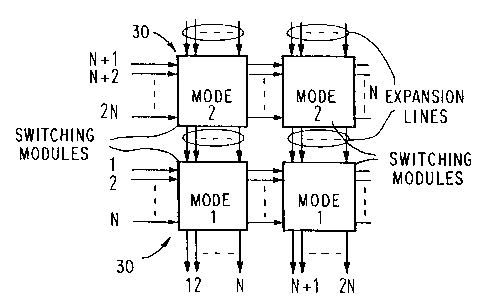
In detail and as depicted in Fig. 4, the present
invention provides that, instead of the two types of switching
modules, a single type of switching module 30 with a storage
function is provided, which can be operated in two different
operating modes 1 and 2 (also turned M1 and M2) as a pre-
switching module or as a final switching module, respectively,
and has N first inputs, N expansion inputs, N first outputs
and N expansion outputs. A first operating mode Ml realizes
the function of the switching module as a final switching
module for the switching of N first input lines and N
expansion input lines to N first output lines, and a second
operating mode M2 realizes the function of the switching
module as a pre-switching module for the pre-switching of N
first input lines and for connecting through N expansion input
;~~o~~~~
lines. The switching module functioning as a pre-switching
module can read in 2N packets simultaneously and read out N
packets simultaneously. The switching module functioning as
a pre-switching module processes with its header information
filter only a part of the header information for switching the
packets to the respective switching matrix column, so that the
lines of the matrix column are shared by packets for this
matrix column. To avoid so-called packet overtaking, the
chronological sequence of packets arriving in each case on one
of the N first input lines of the switching module functioning
as a pre-switching module is replaced from case to case by a
spatial ordering on the N first output lines of the switching
module functioning as a pre-switching module. The switching
module functioning as a final switching module can read in 2N
packets simultaneously. The switching module functioning as
a final switching module processes with its header information
filter another part of the header information for the final
switching to a matrix output.
The chronological sequence of packets, which is lost in
the case where packets are read out from the store of the pre-
switching module in a single packet cycle, is replaced by the
spatial ordering in such a way that the packet read into the
store first is output via the first output line having the
highest priority, that is that line which is processed in the
next respective row of the switching network by the store of
the respective switching module as the first of all N
expansion input lines, the second packet via the first output
line with the second highest priority, and so forth, as a
result of which the chronological sequence of the packets is
recovered.
200039
The switching module has an associated logic circuit 40
which can set via at least one external control connection the
first operating mode M1 or the second operating mode M2.
The spatial ordering is created by means of a logic
circuit assigned to the store in the respective switching
module.
The packets arriving on the input lines with different
packet phases are brought into a common packet phase position
before processing in the respective switching module.
The invention is not limited to the particular details
of the apparatus depicted and other modifications and
applications are contemplated. Certain other changes may be
made in the above described apparatus without departing from
the true spirit and scope of the invention herein involved.
It is intended, therefore, that the subject matter in the
above depiction shall be interpreted as illustrative and not
in a limiting sense.