Note: Descriptions are shown in the official language in which they were submitted.
-
DROP-OUT COMPENSATION SYSTEM FOR HIGH-DEFINITION VIDEO SIGNAL
BAC~GROUND OF THE INVENTION
Field of the Invention
This invention relates generally to a recording
and/or reproducing apparatus for wide band video signals
and, more particularly, to a system for compensating
drop-outs during playback of such signals.
DescriPtion of the Backqround:
A multi-channel recording system has been
proposed for recording wide-band video signals having a
luminance signal bandwidth of about 20 MHz and a
chrominance signal bandwidth of about 6 MXz on an optical
disc. Such wide-band video signals are found in the so-
called high-definition television (HDTV). The video
signals are encoded prior to recording and are
distributed into plural channels and then recorded on
parallel tracks formed in correspondence to the plural
channels. The reproduced signals are decoded back to
original video signals in a reproduction mode. Through
use of this system, even though the rotational speed or
the recording medium is not high, the rate of recorded
infor~ation per unit time is increased by the number or
recording channels. Therefore, a wide-band video signal
can be recorded and reproduced using known record media
and associated hardware.
If there are two channels, a pair of parallel
tracks are spirally formed on a disk. More specifically,
the video signals are simultaneously recorded by optical
Z'~6S~3 35673
heads arranged in parallel relative to the corresponding
tracks for the two channels during the recording mode.
Subsequently, the video signals are simultaneously
reproduced from the tracks by the parallel optical heads
in a reproducing mode.
It has been found that degradation of an image
due to a signal drop-out caused when high-definition
video signals are reproduced tends to be more conspicuous
compared with the effects of such drop-outs when normal
video signals are reproduced.
In order to compensate for drop-outs a system
has been conventionally employed in which a one
horizontal scanning period (lH) memory, or lH delay line
is provided. Upon the occurrence of a dropout, the drop-
out signal portion is compensated by signals of the
immediately preceding line, which have been accumulated
in the lH memory or delayed in the lH delay line.
Although this system is relatively simple, if drop-out
compensation is performed in an oblique line portion of
the reproduced image, 2 discrete step may undesirably
appear in that oblique line of the reproduced image
because of the repeating of the preceding line data.
In another compensation system, a 3H memory is
used, wherein if a drop-out occurs, compensation is
performed by using the mean value of the memory contents,
which are based on the immediately preceding line and
succeeding line periods of the drop-out line interval.
When this system is employed, a discrete step in the
~ 503 35673
oblique lines of the reproduced image is not so
conspicuous as in the case of the lH memory.
Nevertheless, some degradation of the image is still
present. Such degradation is still unacceptable in high-
definition television.
SUMMARY OF THE INVENTION
Accordingly, it is an object of the present
invention to provide a drop-out compensation system that
overcomes the drawbacks inherént in previously proposed
systems.
It is another object of the present invention
to provide a drop-out compensation system for a video
disk recording/reproducing system in which a 3H memory is
used and a recording video signal is divided into two
channels.
In a video disk recording system according to
one aspect of the present invention, a video signal is
alternately divided into two channels in units of one
horizontal interval (lH), and the divided video signals
are time-expanded to obtain continuous signals for
respective channels. At the same time, the timing of
recording video lines on one channel is displaced
relative-to that one the other channel by an integral
multiple of lH, these video signals are then recorded on
a pair of parallel spiral tracks for the two channels.
In a video disk reproduction apparatus
according to another aspect of the present invention, the
. ~06~3 35673
video disk reproducing apparatus comprises a decoding
circuit for time-compressing the signals reproduced from
thè two channels, and correcting the above-mentioned
timing displacement, to obtain the original form of the
sequential frames of the video signal. A compensation
circuit, arranged in each channel, forms a drop-out
compensation signal approximated to the signal of one
channel by an interline mean value of the reproduced
signals of the other channel, and a drop-out correction
circuit detects a drop-out of the reproduced signals from
one channel and substitutes the drop-out portion in the
line sequential signal by the compensation signal
obtained from the other channel.
Since the video signal is alternately divided
into two channels in horizontal scan line units, a
dropout compensation signal approximated to one channel
can be formed from another channel by an interline mean
value signal derived from the reproduced signals. In
addition, because a timing displacement, which may be
thought of as a skew, is formed between the channels,
even if a drop-out has occurred in one channel there is a
low probability that the compensation signal formed from
the other channel will be adversely affected by the drop-
out. Therefore, satisfactory drop-out processing can be
performed by signal compensation in accordance with the
present invention. Since this compensation is mean value
compensation, oblique lines of an image are maintained
continuous in compensated portions in the reproduced
2~06~Q3 35673
image. A high-guality reproduced image compatible with
the goals of HDIV is obtained.
The above and other objects, features and
advantages of the present invention will become apparent
form the following detailed description of illustrative
embodiments thereof to be read in conjunction with the
accompanying drawings, in which like reference numerals
represent the same on similar elements.
BRIEF DESCRIPTION OF THE DRAWINGS
Fig. 1 is a schematic in block diagram form of
a portion of a recording system of a high-definition
video disk recording/reproduction apparatus to which the
present invention is applied;
Fig. 2 is a pictorial representation showing a
track format of a video disk;
Figs. 3A-3E are timing charts of video signals
showing a recording format;
Figs. 4A and 4B are timing charts of video
signals showing a recording formzt;
Fig. 5 is a schematic in block diagram form of
a portion of a reproduction system in a high-definition
video disk system to which the present invention is
applied;
Figs. 6A, 6B, 6I, 6W, 6X, and 6Z are timing
charts of video signals useful in explaining reproduction
processing;
_ Z~6S~3 35673
Fig. 7 is a schematic block diagram form
showing a detailed arrangement of a processing circuit;
Figs. 8A-8I are timing charts useful in
explaining decoding processing;
Figs. 9A,9C, 9F, and 9I, 90 are timing charts
useful in explaining drop-out processing; and
Figs. lOA, 10, lOI, and lOF, and lOV are timing
charts useful in explaining drop-out processing.
DETAILED DESCRIPTION OF THE PREFERRED EMBODIMENT
In Fig. 1 a main encoder portion of a recording
system for a high-definition video optical disk
recording/reproduction apparatus to which the present
invention is applies is shown. Fig. 2 represents a track
format used in such video disk. The video disk 1 is of
the optical type, and may be a disk which allows
recording, reproduction, and erasure, or a disk which
allows the recording operation only once and in which
data therein cannot be erased, or it may be a pressed,
reproduction-only optical disk.
In disk 1, two tracks, representing first and
second channels (CH-1 and CH-2) are spirally formed, so
as to be parallel to each other from an inner periphery
to an outer periphery of disk 1. The track pitch between
the tracks corresponding to the two channels may be 1.5
~m, for example. Two laser beams are modulated by video
signals, and the modulated signals are simultaneously
recorded in the two channels, so that pits corresponding
2~6S~3 35673
to the modulated F~ carrier are formed on the respective
tracks. An incoming single frame video signal is
recorded on the two tracks corresponding to the two
channels. When the angular velocity of the disk is
constant, 1,800 rpm for example, one frame of video
signal is recorded upon each revolution of the disk.
The space (rotational pitch) between each
second-channel track (CH-2) and the adjacent first-
channel track (CH-l) is 1.67~m, for example. However,
since interference due to crosstalk hardly occurs because
of the correlation of video data between the channels,
the space between each pair of parallel tracks can be
made smaller than the track pitch, which was 1.5 ~m.
Therefore, the recording density in this case is higher
than that obtained when all the tracks are formed having
equal pitch. Thus, the track pitch between the chznnels
can be decreased to about 1.1 ~m in correspondence with
the degree of correlation of the signal being recorded.
In this fashion, the recording time can be increased by
about 20~. ~en the degree of correlation changes 2
great deal in one disk, a track interval between the
channels may be varied in correspondence with the degree
of correlation.
The audio signal that corresponds to the video
signal can be recorded in a form of time-compressed PCM
signals during the vertical blanking period of the video
signal.
~ 65~3 35673
On the reproduction side, three laser beams are
used, and focus and tracking operations are performed by
the central beam, with the data in the two tracks being
simultaneously read by the two side beams.
As represented in the waveform charts of Figs.
3A to 3C, the video signal to be recorded includes a
luminance signal, Y of Fig. 3A, having a bandwidth of
20MHz, and a red chrominance signal, P~ of FIg. 3B, and a
blue chrominance signal, P~ of Fig. 3C, each having a
bandwidth of 6MHz. As shown in Figs. 3D and 3E, the
luminance signal Y is time-expanded to be 5/3 times the
original signal, and the expanded signals are alternately
recorded on the channel tracks CH-l and CH-2 on the disk.
In this case, each first channel includes the
corresponding one of the odd-numbered luminance lines
(Y" Y3, . . . ), and each second channel includes the
corresponding one of the even-numbered luminance Y lines
(Y2, Y4, ~--)-
The chrominance signals B and R are
resp~ctively time-compressed by l/2, and are time-
division multiplexed (TDM) with the luminance signal Y.
At this time, the even-numbered lines (B2, B4, ...) of the
chrominance signal B and odd-numbered lines (R1, R3, ...)
of the chrominance signal R are eliminated and not
recorded and the odd-numbered lines (Bl, B3, . . . ) of the
chrominance signal B and even-numbered lines (R2, R4, ...)
of the chrominance signal R are respectively divided into
two channels for recording. Therefore, in each track,
~ 6S~3 35673
the two chrominance signals R and B are alternately
arranged in a line-sequential manner.
As shown in Figs. 3A-3E, lH on the disk
corresponds to 2H of the recording signal. When the Y
signal is time-expanded by 5/3 times, the maximum
recording frequency at the baseband is decreased from 20
MHz to 12 MHz. When the chrominance signals are time-
compressed by 1/2 times, the recording frequency at the
baseband is increased from 6 MHz to 12 MHz. Therefore,
on the disk, the Y, R, and B signals each having a
bandwidth of 12 MHz are recorded in the form of FM
modulation.
In order to per~orm satisfactory drop-out
compensation in a manner to be described below, a 4H (2H
on the disk) skew is provided between the first and
second channels, as shown in the format in Figs. 4A and
4B. In this embodiment, the recording operation in the
~irst channel is delayed from that in the second channel
by 4H.
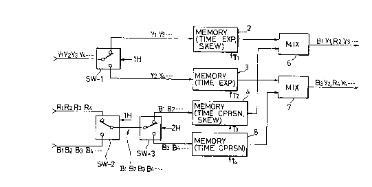
In the block diagram of Fig. 1, an encoder is
shown for converting input video signals in accordance
with the above-mentioned recording format, that is,
channel division, channel skew, and time expansion and
compression. The input luminance signal Y is divided
into the first channel (Y1, Y3, . . . ) and second channel
(Y2, Y4, . . . ) by a branch switch SW-1 switched at every
horizontal line interval (lH), and the signals are
written in time expansion memories 2 and 3, respectively.
. ,
. 2~065~3 35673
the contents of memories 2 and 3 are time-expanded in
response to a read-clock signal having a frequency that
is 3/5 times that of a write-clock signal and are
respectively read out in response to timing signals T1 and
T2 ~ ,
On the other hand, the input chrominance
signals R and B are fed in parallel to a selection switch
SW-2 and alternately switched at every H interval so that
the B signals in the odd-numbered lines and the R signals
in the even-numbered lines are alternately selected and
output, thus obtaining a serial signal (B1R2B3R4...). This
line sequential signal is divided into the first channel
(B1R2...) and the second channel (B3R4...) by a branch
switch SW-3 switched at every 2H interval, and the
divided signals are written in time compression memories
4 and 5, respectively. The contents of memories 4 and 5
are time-compressed in response to a read-clock signal
having a frequency two times that of a write-clock
signal, and are respectively read out in response to
timing signals T3 and T4.
The read timings of memories 2, 3, 4, and 5 are
respectively controlled in response to the timing signals
T1, T2, T3, and T4 to achieve a time-divisional
relationship therebetween, as represented in Figs. 3D and
3E. The first channels are mixed by a mixing circuit 6
and the second channels are mixed by a mixing circuit 7,
so that a pair of parallel signals for two channels of
--10--
35673
Z.~ iS~33
B1Y1, ~Y3, ..., and ~Y3, R4Y4, ..., are generated as shown
in Figs. 3D and 3E.
Memories 2 and 4 for the first channels have a
channel s~ew function and cause output timings of the
luminance and chrominance signals in the first channels
to be delayed from those in the second channels by 4H.
As a result, wide-band video signals are recorded on the
disk 1 in the format shown in Figs. 4A and 4B.
Fig. 5 is a block diagram of a reproduction
system, and Figs. 6A-6Z are timing charts for
reproduction processing. As described above, the pair of
parallel tracks on the disk 1 are simultaneously read by
a parallel beam pickup head. The reproduced signals are
obtained from two photodetectors 10 and 11 for the two
channels and are respectively supplied to FM demodulators
14 and 15 through RF amplifiers 12 and 13. The
demodulated video outputs are then converted into digital
signals by A/D converters 16 and 17, respectively.
Signal processing is performed in response to
the digital signals as follows. Digital video signals a
and b for each channel, respectively shown in Figs. 6A
and 6B, are time-base corrected by time base correctors
18 and 19 to obtain a line sequential serial signal i
shown in Fig. 6I from a mixing circuit 20. Mixing
circuit 20 has a function for compressing the time base
of the signals in each channel by 1/2, correcting their
skews, and decoding line sequential format as shown in
Fig. 6I. Since this function can be realized by a memory
Z~065~3 35673
of several lines, the line memories for time base
correctors 18 and 19 may have the function of mixing
circuit 20 in a modified embodiment.
Mixing circuit 20 also has a drop-out
compensation function utilizing the line memories. More
specifically, a drop-out of the disk reproduced signal is
detected by a drop-out detector 21 for respective
channels in response to outputs from RF amplifiers 12 and
13. Drop-out detection signals DO1 and DO2 are supplied
to mixing circuit 20 as compensation control signals
through a delay circuit 22. During a drop-out period,
mean value compensation signals formed on the basis of
the outputs from the line memories are output in place of
the drop-outs in the reproduced signals.
The line sequential signal i output from mixing
circuit 20 is separated into a luminance signal Y and
chrominance signals R and B by a separator 23, and the
separated signals are time-expanded to obtain normal
time-base signals w and x, shown in Figs. 6W and 6X, by Y
and C expansion circuits 24 and 25, respectively. The
expansion ratio of the Y expansion circuit 24 is 6/5
times, and the expansion ratio of the C expansion circuit
25 is four times. Outputs form expansion circuits 24 and
25 are subjected to analog processing such as frequency
and amplitude adjustment by Y and C signal processors 26
and 27, respectively. As shown in Figs. 6Y and 6Z, in C
signal processor 27 the line sequential signals B and R
are separated into parallel signals, and the R and B
S5~)3
35673
signals in the odd-numbered and even-numbered lines that
were eliminated upon recording are regenerated by an
interpolation process based on the preceding and
succeeding video lines.
Outputs from signal processors 26 and 27 are
supplied to D/A converters 28, 29, and 30, so that the
luminance signal Y, and the chrominance signals B and R
are obtained.
In regard to the audio portion, a PCM signal
recorded during a vertical blanking period is extracted
from the outputs supplied by FM demodulators 14 and lS by
separators 31 and 32. The separated audio signals are
respectively subjected to time-base correction and time
expansion by time-base correctors 33 and 34, and are
subjected to digital signal processing such as PCM
decoding, deinterleaving, error detection, error
correction, and compensation by a decoding error
correction circuit 35.
An output from decode error correction circuit
35 is frequency band-limited by a filter 36, and the
band-limited signal is divided into analog audio signals
L and R for the two channels by a separator and D/A
converter 37.
Fig. 7 shows a detailed arrangement of mixing
circuit 20 of Fig. 5, in which line memories and delay
circuits to perform time compression, decoding of
alignment of the signals divided into two channels, skew
correction, and generation of drop-out compensation
-13-
~65V3 35673
signals are provided. The line memories and the delay
circuits can be realized by RAMs and address controllers,
or the line memories in the time base correctors 18 and
19 may be utilized in the alternate embodiment.
It should be noted, relative to Figs. 9, and
10, that the ratios of the time widths for Y and R or B
are not to scale because of size limitations of the
drawings. The time width of the luminance portion is
greater than the chrominance portion.
Playback signals a and k, which are the time
base corrector outputs, for the respective channels shown
in timing charts Figs. 8A and 8B are respectively
supplied to Y/C separators 40 and 41. The time-division
multiplexed components Y and C are separated, and the
separated components are written in line memories 42 to
45, each having a period of 2H on the disk. The written
components are time-compressed to 1/2 by reading out in
response to a read-clock signal having a frequency twice
that of the write-clock signal. Figs. 8C and 8F show
time compression outputs. Although the components Y and
C (B and R) are not separated in Figs. 8C and 8F for the
sa~e of descriptive convenience, the components can be
separated, as shown in signal paths in Fig. 7, or the Y
and C signals may be separated after time compression.
In the first channel, a B signal portion in the
output from line memory 42 is derived through a 3H delay
circuit 46, and an R signal portion is derived through a
2h delay circuit 46, and an R signal portion is derived
-14-
~06S~3 35673
through a 2H delay circuit 47. These signals are mixed
again, as shown in Fig. 8D. The 2H and 3H delays may be
realized by control operations of read timings of line
memory 42. The Y signal output from line memory 43 is
output through a 3H delay circuit 48, as represented in
8E.
In the second channel, in the same manner as in
the first channel, a B signal portion in an output from
line memory 44 is derived through a 9H delay circuit 49,
and in R signal portion is derived through an 8H delay
circuit 50. These signals are mixed again, as shown in
Fig. 8G. The Y signal output from the line memory 45 is
output through an 8H delay circuit 51 (Fig. 8H).
Outputs d, e, g, and _, from the delay circuits
46 to 51 are respectively supplied to U contacts of
switches SW-11, 12, 13, and 14, and are com~ined by
commonly coupling the movable contact outputs-from the
switches, thus being output as the line sequential
reproduced signal i shown in Fig. 8I. The delay circuits
46 to Sl have delay amounts to correct skews of p~irs of
parallel signals for two channels and to decode the
parallel signals into a line-sequential serial signal.
Outputs form line memories 42 and 45 are also
supplied to the mean value compensation circuit. More
specifically, a B signal portion derived from line memory
42 in the first channel is delayed by a lH delay circuit
52 by lH, and is coupled to a non-delayed R signal
portion, as shown in Fig. 9J. A composite signal i is
~Q65~3 35673
supplied to a 4H delay circuit 53. A delay output k
(Fig. 9K) from delay circuit 53 is added to the input i
thereto by an adder 54, and is level-decreased to 1/2, so
that a mean value signal, shown in Fig. 9L, is formed.
The Y signal output from line memory 43 in the
first channel is delayed by a 2H delay circuit 55, as
shown in Fig. 9M. An input c to the circuit 55 is added
to an output m therefrom by an adder 56, and the sum is
averaged, thus forming a mean value signal n shown in
Fig. 9N. This signal n is further delayed as a signal o
by a 2H delay circuit 57 (Fig. 90).
Compensation signals 1 and o formed by mean
value processing are respectively supplied to D contacts
of the switches SW-11 and SW-12. When a drop-out has
occurred in the second channel the drop-out detection
pulse DO2 is supplied to these switches SW-ll and SW-12
as a switching signal, and the mean value compensation
signals 1 and o are respectively output from the switches
in place of the reproduced signals a and e.
As shown in the 'iming chart for drop-out
compensation in Fig. 9, when reproduced signals R52 and
U52, as shown in Fig. 9B, in the second channel are
dropped out, the drop-out portions are compensated by
mean value compensation signals R52 and Y52 formed by the
above-mentioned mean value circuit on the basis of
reproduced signals R50 and R54, Y51 and Y53, as shown in
Fig. 9A, of the first channel side, as shown in Fig. 9I.
Since the corresponding portions in each channel are
-16-
~ 65~3 35673
shifted in the longitudinal direction of the track due to
the 4H channel skew, the drop-out in one channel can be
accurately compensated by a normally reproduced signal
from the other channel.
Similarly, a drop-out in the first channel is
compensated on the basis of the reproduced signal from
the second channel. More specifically, the B signal
portion in the output from line memory 44 in the second
channel is delayed by a lH delay circuit 58 by lH, and is
coupled to a nondelayed R signal portion, as shown in
Fig. lOP. A composite signal ~ is supplied to a 4H delay
circuit 59. A delay output ~ (Fig. lOQ) from delay
circuit 59 is added to an input p thereto by an adder 60,
and the sum is level-decreased to 1/2, so that a mean
value signal _, shown in Fig. lOR, is formed.
The Y signal output from line memory 45 for the
first channel is delayed by a 2H delay circuit, as shown
in Fig. lOT. An input f to delay circuit 62 is added to
an output t by an adder 63, and the sum is averaged, so
that a mean value signal u, shown in Fig. lOU, is formed.
This signal u is further delayed as a signal _ by a 7H
delay circuit 64, as shown in Fig. lOV.
Compensation signals s and _ formed by mean
value processing are respectively supplied to D contacts
of switches S-13 and SW-14, and are output in place of
the reproduced signal i when a drop-out has occurred in
the first channel.
~ 35673
- 2~ 503
~ As shown in the timing chart of Fig. 10, when
reproduced signals R46 and Y47, as shown in Fig. lOA, in
the first channel are dropped out, the drop-out portions
are compensated by mean value signals R46 and Y47 formed
on the basis of normally reproduced signals R44, R48,
Y46, and Y48.
It will be noted that of switches SW-11 to SW-
14, switches SW-11 and SW-12 for the first channel are
controlled by the drop-out detection pulse D02 of the
second channel, and switches SW-13 and SW-14 for the
first channel are controlled by the drop-out detection
pulses DOl of the first channel. The drop-out detection
pulses DOl and D02 are supplied to the switches as
switching control signals after an optimal delay time and
a pulse width are given thereto.
As described above, in the present invention,
video signals are alternately divided into two channels
in units of lines, and the divided channels are recorded
on the disk as spiral parallel tracks for the two
channels. Recording operations in the channels are
simultaneously processed (in parallel) without using
field memories in both the recording and reproduction
systems. Signal processing for recording/reproduction
can be performed by using a memory of only several lines.
An interline mean value of one channel can form a
compensation signal approximating the other channel.
Since timing displacement (skew) is provided
between the channels during the recording operation, upon
-18-
~ 503 35673
occurrence of a drop-out in a reproduced signal in one
channel there is a low probability that a compensation
signal produced from the other channel for the drop-out
portion would be damaged due to that drop-out.
Therefore, as the signal compensation is performed from
one channel to the other channel, satisfactory and highly
reliable drop-out compensation can be achieved.
Furthermore, because a mean value compensation
is performed, discontinuous oblique lines do not appear
in an image so that degradation of the image quality can
be avoided.
Also, although in the above-described
embodiment, the control (CTL) signal is used to detect
the tape position, the method of detecting the tape
position need not be so limited and any other signal
corresponding to a CTL signal could be used for such
purpose.
The above description is given on a single
preferred embodiment of the invention, but it will be
apparent that many modifications and variations could be
effected by one skilled in the art without departing from
the spirit or scope of the novel concepts of the
invention, w-hich should be determined by the appended
claims.
--19--