Note: Descriptions are shown in the official language in which they were submitted.
oz~
~`
DANFOSS A/S, DK-6430 NORDBORC
-:
Inverter circuit and a method for controlling same
.; The invention relates to an inverter circuit whlch converts ~;
d.c. from a d.c. source to at least single phase a.c., compris-
ing two semiconductor switching elements ror each phase connec-
ted in series between the two poles Or the d.c. source, wherein
a recovery diode inparallel with each semiconductor switching
element is disposed in the blocking direction in relation to
the d.c. source and an a.c. outlet is disposed between the two
semiconductor switching elements, and comprising a control
circult for operating the semiconductor switching elements
with a pulse width-modulated operating signal. The lnvention
also relates to a method Or operating an inverter clrcuit which
~I converts d.c. to at least single phase a.c. and ln each phase
.~ , ,
comprises two semLconductor switching elements with parallel-
connecte,i recovery diodes connected between the two poles Or ~ ~-
the d.c. source, wherein the a.c. can be derived at an a.c.
outlet between the two semiconductor switching elements and the I
latter are operated with a pulse width-modulated operating
signal.
A known lnverter circuit (US-PS 4 617 622) is operated with a
pulse width-modulated signal and a control clrcuit. The
; .
~ signal o~ this control circuit can assume the lo6ic values zero
~.
~ .
7~23
. ,
,: ~
,
,.
and one. At the value one, the semiconductor switching element
connected to the plus pole of the d.c. source is brought to a
conductive state and the semiconductor switching element conne-
cted to the minus pole is brought to a blocked state, the
reverse being the case for the value zero. Operatlon takes
place by way of the rising or falling flank of the operating
signal. The scanning ratio, i.e. the ratio Or the duration in
one period for which the signal has the value one to the entire
lenght of the period governs the voltage at the a.c. outlet.
The voltage at the a.c. outlet referred to the voltage Or the
' negative pole Or the d.c. source corresponds to the voltage
; dlfference between the two poles of the d.c. source multiplied
by the scanning ratio. Ir, ror example, the d.c. source is
¦ constructed symmetrically, i.e. the voltage Or the negative
I pole amounts to exactly the same as the voltage of the positive
I pole, the voltage zero is obtained at the a.c. outlet with a
scànning ratio of 0.5. By means Or variations in time ror the
scanning ratio, e.g. in the form Or a sine curve, one can
achieve a variation in the time for the output voltage Or the
.
inverter, provided that the period Or pulse width-modulation is
considerably shorter than the period Or the sine curve. In
other words, the modulation rrequency must be substantially
hlgher than the frequency of the a.c..
, ~ ` , ' :
I In the ideal case, the inverter output voltage is exactly
:. -:
, proportional to the scanning ratio Or the pulse width-modulated
oz3
signal. In reality, however, all controllable semiconductor
switchine elements require a certaln time to switch Orr. This
switching off period is calculated from the instant at which
the switching element is to be brought to the switched-ofr
condition by the operating signal, e.g. by a transition from
the value one to the value zero, up to the instant at which the
current through the switching element disappears, i.e. the
switching element is indeed bloclced. In contrast, the switch-
ing on period, i.e. the time before arrival of the "operating"
signal, e.g. by a rising flank Or the operating signal from the
value zero to the value one, up to reaching the full current is
markedly shorter. This phenomenon i9 particularly apparent
ror certain types of bipolar transistors.
::
In US-PS 4 617 622, each control line therefore includes in
rront of each semiconductor switching element retarding means
which delay the ignition, i.e. opening or operation, Or the
semiconductor switching element by a time which must be at
least as large as the switching off period of the other switch-
ing element. If the delay period were to be shorter, the one
switching element will be operated whilst the other is not yet
closed and for every operation there would be a short circuit
between the two poles of the d.c. source. To avoid undeAirable
harmonics, a f`urther retarding element is introduced in the
signal path Or the pulse width-modulated operatlng signal, its
.~
,:. .~ ,' ' . ';' . ~ ' . ,
! ~ O ~ ~ OZ3
., .
~.
.
-4- ~
." ~
delay being variable and being reduced proportionally to the
,~ load current. With a positive current, the delay takes place
~ only at the falling flank and with a negative current only at
A' the rising flank. This system is particularly 3uitable for
compensatlng a linear current dependency in the swltchlng off
period of the semiconductor.
,~, '
.;,~ ..
The swltching off period of the semiconductor swltching elements
vary over a large range depending on many factors, including
the type and make of semiconductor, statistic scatterlng, i.e.
dirrerences between indlvidual specimens of semiconductors Or
the same type and the same make, temperature variations, the
switchlng off perlod being higher with a rise ln temperature,
and load current. In addition, there must be an adequate
safety margln, whereby the ignition delay in most operating
conditlon~ Ls conslderably longer than the actual switchlng off
period of the semiconductors. Conventionally, each retarding
means retards the operating signal by a period which is three
to four times larger than the actual switching Orr period of
1 ~ , I ` ; ' ~ " '
~- the semiconductor.
However, the excessively long retardation results in the actual
scanning ratio no longer correspondlng to the de~red scanning
ratio. Accordingly, the inverter output voltage no longer
71 exactly rollows the predetermined course but is smaller than
~ desired for a po3itive direction of current at the inverter -~
~ , ; .
1 ~0~3Z3
output and larger than desired for a negative direction Or
current at the inverter output. Positive current directLon
means that the current flows out of the inverter output when
the switchlng element is open or operated and negative direction
of current means that it flows into the inverter output. With
an ohmic load on the inverter, i.e. no phase displacement
between the current and voltage (cos ~ = 1), the amplltude of
the a.c. output voltage is reduced relatively to the predeter-
mined value, whereas with an inducted load (C09 ~ = 0), the
amplitude of the output voltage corresponds to the predetermined
voltage.
.
This phenomenon is of particular disadvantage when operati~ng
asyncronous motors with variable rrequency. Especially at low
rrequencies where the amplltude Or the voltage Or the basic
wave is also low, even a small voltage loss will be found
disruptive because the torque Or the motor is very much reduced
at an excessively low voltage. However, it will be known that
especially on starting from standstill a high torque is desi-
I rable. Normally, the problem is resolved by correcting the
scanning ratio of the pulse width-modulated operating signal in
the control circuit so that the voltage is increased. This
alleviates the problem Or an excess Or the low torque but
causes the motor to be fed with an excess of the high voltage
1 ~01~3Z3
--6--
in the unloaded condition because cos ~ drops when the torque
is reduced. This, in turn, results in the motor requiring an
inappropriately hlgh idling current at a low frequency, thereby
increasing the danger of overheating. Conventional IxR compen-
sation at which the voltage i9 increased depending on the load
current will not solve the problem because there is no clear
relationship between current and cos f . It has also been
tried to reduce the modulation frequency Or the pulse width-
modulated operating signal. However, this leads to higher
losses and more noise in the motor, so that it i3 still pre-
ferred to keep the modulation frequency as high as possible.
~, ,
For this reason, it is the problem Or the present invention to
provide an inverter circuit of the aforementioned kind that
produces the predetermined output voltage independently Or cos
gLven by the load and independen,tly Or the direction of
current.
.. . . .
This problem is solved in an inverter circuit of the aforemen-
tioned kind in that the control circuit controls with the
operating signal only the semiconductor switching element of
one phase into a pass condition which connects that pole of the
d.c. source to the a.c. outlet Or which the polarlty corresponds
to that Or the current rlowing at the a.c. outlet, and the
.
other semiconductor switching element blocks lndependently Or
the operating signal.
.
. , ;,~:
2007023
6a
Specifically, the invention relates to an inverter
circuit for converting d.c. from a d.c. source having
positive and negative poles to al least single phase a.c.,
,i comprising: first and second sem:iconductor switching elements
for each phase connected in series between the poles; an a.c.
output between the switching elements; recovery diodes in
respective parallel relation to the switching elements
disposed in blocking directions relative to the d.c. source;
signal generating means providing a pulse width modulated
operating signal for operating the switching elements; first
~ and second blocking means for effecting respective control of
; the switching elements with each of the blocking means having
, an input effectively connected to the signal generating means
and respective outputs respectively connected to the first
and second switching elements; and control means including
current directing sensing means responsive to current flow at
the a.c. output for selectively effecting nonblocking of the
j first and second blocking means in accordance with the
direction of current flow at the a.c. output; the control
means operating to effect nonblocking of both of the blocking
means when the current flow at the a.c. output is in a narrow
range on both sides of zero.
i
~ ,
rn/
:'
3 ~ ~
!~2c~7Uz3
!
-7-
Thus, according to the invention, no short circuits can occur
between the positive and negative pole of the d.c. source.
Accordingly, the semiconductor switching elements can be operat-
ed without regard to the possible occurence of a short clrcuit
situation. It is therefore not necessary to provide an excess-
ively long delay in the signal path of the operating signal for
changing the scanning ratio, whereby the output voltage can
more accurately ~ollow the desired course. Since no voltage
losses are created, there is also no dependence Or such losse
on cos~ or on the current direction.
, .
In A prererred embodiment, the contrtol circuit comprises block-
in~ means which are either released by a control logio dependin~ ;
on the polarity Or the current at the a.c. outlet to operate
the operating signal at the semiconductor element or are block-
ed. Ir the blocking means are released, they open a signalling
path for the operating signal which can then influence the
control electrode Or the semiconductor s~itching element.
I This embodiment enables a very simple control to be achieved
for the inverter circuit. The operating signal can be produced
~ in the same way as hitherto. No complicated changes are
¦~ necessary at the operating signal generator. If undeslrable
¦ because of the condition of the circuit, the operating signal
is simply not permitted to pass to the 3emiconductor switching
element. -~
.~. ,
I ~OI~V;;~3
Advantageously, the blocking means are in the form of AND gates
of which the outlet communicates with the respective control
electrode of the associated semiconductor switching element of
which the one lnlet is influenced by the operating signal for
the assiociated semiconductor switching element and the other
input in influenced by an outlet signal of the control logic.
AND gates are particularly easy ~o use as blocking means. As
long as the one inlet is influenced by a correspondlng signal,
for example a logic one7 the signal of the other inlet will ~`
appear at the outlet. On the other hand, if the AND gate at
the first inlet is fed with the logic value zero, the value
zero will also appear at the outlet, regardless of the cause of
the signal at the other inlet.
With advantage, a respective retarding means disposed between
each blocking means and the associated semiconductor switching
element retard~ by a predetermined delay period that part of
the operating signal which brings about operation of the semi-
conductor switching element. The part Or the operating signal
which operàtes the semiconductor element is for example the
rising flank for the semiconductor switching element connecting
the positive pole of the d.c. source to the inverter outlet and
for example the falling flank of the operating signal for the
other semicontluctor switching element which connects the neaa~ve ;~
pole Or the d.c. source to the inverter outlet. This con-
~::
t
I ~0~7VZ~
.,. ~ .
_9_
struction has the following advantage. When the switching on
period, i.e. the time from arrival Or the respective flank Or
the operatlng signal up to full current flow is substantially
shorter than the switching off period, the scanning ratio would
become larger than desired, with the result that there is
an excessively high output voltage at the lnverter outlet. By
incorporating a delay period, this phenomenon can be compensated
to a large extent.
'
Advantageou31y, the retarding means can be changed over between
a shorter and a longer delay period. As already mentioned,
the switching off period depends interlalla on the aurrent
strenght. Depending on the load, one can then select a shorter
or a longer delay period for the switching off compensating
period ir the dependence of the switching off period Or differ-
ent currents is to be taken into consideration.
,
However, it is particularly preferred for the change-over to be
carried out by the control logic depending on the polarity of
the current at the inverter outlet, the retarding means for the
semiconductor switching element which is to be driven to the
pass condition being changed over to the shorter delay period.
This ensures that it will always be the switching element which
i8 to be momentarily conductlve that will be influenced by the
shorter delay period. If an error causes the other semicon-
,ductor switching element to be changed over during the next
~ . ....
I éo 3,~z~
--10--
change Or the level of the operatine sienal, l.e. during a
rising or falllng flank, changing over will there take place
over a correspondingly longer delay period so that here, too, a
short circuit condition can be reliably avolded.
In a narrow range Or current about zero, it is often difricult
to determine the polarity of the current. For this reason,
the control logic releases the blocking means of both semicon-
ductor switchlng elements at a value Or the alternating current
in a predetermined range above and below zero. Consequently,
both switching elements are fed with operating signals. No
i losses are likely because the current i5 practically zero.
It is of advantage for the control logic to change the retarding
means over to the longer delay period when both blocking means
are released. For safety reasons, the one semiconductor
swltching element can then ignite only when the other is reli-
ably closed. The losses that can occur during this time are
not, as stated above, significant because practically no current
,' ' is rlowlng. ;~
Advantageously, the control logic comprises means for detecting
the directlon and amount Or the current flowing at the inverter
¦ ~ outlet, and comparator means which produce a releasine signal
¦ for one of the two blocking means when the current is not
! ~0~7~Z3
'I
less than zero and a releasing signal for the other blocking
means when the current is not larger than zero. Both signals
are thererore produced when the current ls substantially zero.
This is a simple way of ensuring that in the narrow range of
the current value around zero both semiconductor switching
elements are operative.
,', ' -:.
Preferably, the releasing signal for the blocking means of the
one semiconductor switching element changes the retarding means
Or the other semiconductor switching element from the shorter
,
to the longer delay period. As a result, at the instant when
both semiconductor switching elements can be fed with operating
signals because both blocking means are released, the longer
delay period will also always be switched on.
'
In a preferred embodiment, the inverter circuit produces a
three-phase alternating current of which the phases are elec-
trically displaced by 120 each. This embodiment is employed
with particular advantage for three-phase a.c. motors, partl-
cularly~ asychronous machines.
In a method of the aforementioned kind, the problem is solved
in that, as long as the current at the inverter outlet has the
one polarity, only that semiconductor switching element is fed
with the operating signal which connects the a.c. outlet to the
i ,' ~
~ pole of the same polarity, whilst the other one remains blocked.
5 ' , . . ' .
1 ~0~7t)2~ i
-12-
A preferred example of the invention will now be described in
conjunction with the drawing in which the single flgure illu-
strates a single phase inverter.
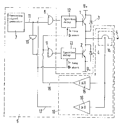
The inverter comprise3 two semiconductor switching elements 1,
2 connected in 3eries between the two poles U , U of a d.c.
source. Parallel to each semiconductor switchlng element 1,
Z there 19 a respective recovery diode 3, 4. Both recovery
diodes 3, 4 are poled in the blocking direction in relation to
the voltage direction of the d.c. source. ~etween the two
semiconductor switching elements, an alternating current can be
tapped at the inverter outlet 5.
Each semiconductor switching element l, 2 is fed with an operat-
ing signal by way of a control circuit 6. The control circuit
6 comprises an operating signal generator 7 which produces the
operating signal 11. This operating signal is a pulse width-
modulated ~ignal with two logic values zero and one. The one
semlconductor switching element 1 whlch connects the posltive
pole U~ of the d.c. source to the a.c. outlet 5 19 brought to a
conductive condltion by a change ln the operatlng slgnal from
the level zero to the level one, i.e. it is ignited or operated,
whereas the other semlconductor swltching element 2, which
connects the negative pole U Or the d.c. source to the a.c.
outlet 5 is ienited or operated by a change in the level ~rom ~
one to zero. After lgnition, the operated semiconductor
.; . .~:
- ' ~ ', ' .:
I ~olE170Z3
.` !
-13~
.~ , .
switching element 1,2 continues to allow current to pass or
remain3 open until the operating signal change3 the level
again, i.e. returns from one to zero for the semiconduetor
l switching element 1 or from zero to one for the semiconductor
, switching element 2. To enable the same semiconductor switch-
; ing elements to be employed, the operating signal for the
,
semiconductor switching element 2 i9 inverted by an inverter
19. However, the falling or rising flank does not immediately
block the respective semiconductor switching element 1, 2 but
only introduces the blocking. Between the occurence of this
flank up to actual blocking, i.e. the cessation of all current
through the respective semiconductor element, there i3 a 90-
called "switching off period".
I, `
The operating signal ll is not applied directly to the ignition
electrodes of the semiconductor switching elements. Every
semiconductor switching element is associated with ignition
retarding means 12, 13 connected to the control electrode of
i~ the respective semlconductor switching èlement 1, 2. The
~ ignition retarding means 12, 13 receive their input signal from
3 blocking means 8, 9 in the form of AND gates. Each gate has
i~ ~ two inlets, one Or whlch is fed with the operating signal 11
from the operatlng signal of the generator ?. The other lnlet
of the blocking means 8, 9 is connected to a eontrol logic 10.
, ~ The control logic 10 produces at an outlet 17 a signal with
the value of logic one when the current is not less than zero,
~ ' :
'
7~Z3
-14-
`i~
i.e. larger or equal to zero. This signal is fed to the
blocking mean3 8 for the semiconductor switching element 1 that
is connected to the positive pole of the d.c. source. The
other outlet of the control logic 10 carrleq a slgnal Or logic
one when the current is not larger than zero, l.e. equal or
less than zero. Th1s signal is fed to the blocklng means 9 of
the semiconductor switching element 2 that is connected to the
negative pole in the d.c. source. If the outlets 17, 18 do
not carry the value of logic one, they will carry the value of
logic zero. To produce the signals at the outlets 17 and 18,
.~
the control logic 10 comprises a current converter 14 which
detects the size and polarity Or the alternating current at the
a.c. outlet 5. The signal obtained by the current converter
14 i~ fed to a diagrammatically illustrated comparator 15 which
determlnes whether the current is smaller or equal to zero and
a likewise diagrammatically illustrated comparator 16 which
determines whether the current is larger or equal to zero.
Both comparators 15, 16 produce a signal level of logic one
`; when the stated comparison is positive, i.e. when the condition
is fulfilled, otherwise a signal level of logic zero.
- The retarding means 12J 13 can be changed over between two
~ ....
differently Long delay periods. This change-over takes place
depending on signals in the outlet lines 17,18 Or the control
, logic 10. If the comparator 15 determines
~ '' ' , ' '
~ ~
I ~OQ~z;~
~15-
that the current is smaller or equal to zero, the delay perlod
Or the retarding means 12 is set to a long value. If it is
determined that the condition Or the comparator 15 has not been
fulrilled, i.e. that the current i9 larger than zero, the
retarding means 12 are set to a short delay period. The
retarding mean3 13 are set to a long delay period when the
comparator 16 detects that the current i~ larger than or equal ~;
to zero. The delay period Or the retarding means 13 is, on ~ ;
the other hand, set to a shorter value when the comparator 16
finds that the value is smaller than zero.
Assume that the inverter i9 to be employed to produce a somewhat
sinusoidal alternating current at the a.c. outlet 5. The
operating signal generator 7 produces a pulse wldth-modulated
operatlng signal 11 which is fed to the two blocklng means 8,
9. The blocking means 8, assoclated with the semiconductor
switching element 1 which connects the posltive pole U of the
d.c. source to the a.c. outlet 5 is only released when the
control logic 10 detects that the current at the a.c. outlet 5
ls larger than or équal to zero. In this case, the operating
slgnal 11 can reach the control electrode of the semiconductor
switching element 1 through the retardlng means 12, whereby the
semlconductor s~itohing element is operated. Current can
therefore flow ~rom the positlve pole of the U+ o~ the d.c.
source to the a.c. outlet 5. A positive current is here
~t~7~z3
. ,
,.,.
.... ~
-16-
X; ~ i
.: ,
created, i.e. a current which flows out Or the lnverter. Depend-
ing on the duration Or the operatlng pulse of the operating
; `
1 signal 11 the semlconductor swltchlng element 1 ls closed agaln
: after a predetermined time. Some!what later, namely after the
. . ~
- switching off perlod has expired, the flow Or current from the ~;;
positive pole U+ Or the d.c. source to the a.c. outlet 5 ceases.
., '!
With an ohmic load, at which the current and voltage are in
phase, the flow Or current ceases altogether. With an in-
ductive load at the a.c. outlet 5, however, the current tends
to continue to flow. So long as the upper semiconductor
i swltching element 1 ls closed, a current will accordingly flo~
~I from the negatlve pole U of the d.c. source through the re- ;
covery dlode 4 lnto the a.c. outlet 5. The lower semiconductor
switchLng element 2 remalns closed all the time as long as a
positlve current flows at the a.c. outlet 5. The scanning
ratio of the operating signal 11 is varied somewhat sinusoidally.
Accordingly, in the positive hal~ wave, the pulses operating
the upper semiconductor switching element 1 are longer than the
pauses between the pulses. The voltagè of the a.c. outlet 5
therefore likewise changes sinusoidally. As long as the
current at the a.c. outlet 5 is in the positive half wave, only
the semiconductor switching element 1 is operated. The semi-
1: . : .
conductor swltching element 2 remains permanently blocked. In ~-j
no case can a short circult take place between the positlve j~
pole U~ and the negative pole U of the d.c. source.
~ ' ,~'`''~.
-
I ~o~az3!
--17--
At the end of the positive half wave, the current at the a.c.
outlet approaches zero. In this range, the current converter
14 can no longer determine reliably whether the current has a
positive or a negative direction. Accordingly, the control
logic produces at both of its outlets 17, 18 a signal with the
logic value of one. Consequently, both blocklng means 8, 9
for the control signal are brought to the pass condition. The
operating signal 11 now reaches the control electrodes of both
semiconductor switching elements 1, 2 by way of the retarding
means 12, 13 which are now both switched to a long delay period.
The semiconductor switching elements are now conventionally
operated for a short period, i.e. for the time required by the
current to leave the narrow range about the value zero in the
negative direction. Thereafter, the current converter 14 can
again reliably determine that only a negative current flows at
the a.c. outlet 5, i.e. the current flows from the load into
the inverter. During the negative half wave, the blocking
means 8 are blocked ror the upper semiconductor switching
element 1 and the operating signal 11 only reaches the semicon-
ductor switching eIement 2 by~way of the blocking means 9 and
the retarding means 12. Both semiconductor switching elements
1, 2 are alternately operated even if the effective value of
~the current at the a.c. outlet i9 substantially equal to zero.
I ~gO~7~ 3
-18-
With an inductive load, there is a phases dlsplacement between
the current and voltage. In this case, lt can happen, that a
positive voltage is applied to the load whilst a negatlve
current i3 flowlng. As long as a negatlve current flows, it
ls immaterlal whether or not the semlconductor swltchlng element
1 can be operated because in this condition no current can flow
through the semlconductor switching element 1. The required
current is in this case fed by way Or the recovery dlode 4
which is connected in parallel to the lower semiconductor
switching element 2. For the converse case, mainly negatlve
voitage with positive current, the current distrlbution is
exactly the opposlte, l.e. the upper recovery diode 3 carrles
the current whilst lt ls lmmaterlal whether or not the lower
semlconductor swltching element 2 can be operated. It is only
when the current has become posltive again, i.e. the semlcon~
ductor switchlng element 1 could àlso carry a current, that lt
wlll be fed wlth the operatlng signal 11 ln order intermittently
to produce a conductive connection between the positlve pole of
the d.c. source U and the a.c. outlet 5.
The retardlng means 12, 13 could in principle also be omltted.
However, since the switching off Derlod ls in most cases larger
; ~ than the switching on period, the scannlng ratlo and thu~ the
outlet voltage of the inverter would become larger than desired.
For this reason, the retarding means 12, 13 have a delay
corresponding to the switching off period of the semiconductor
I ~OIIa7Q~3
-19~
switci1ing elements 1, 2. The delay period must not, however,
be selected to be any greater, whereby excessive dead periods
are avoided. An exception is made in the region where the
current has a value approximately equal to zero. In this
range it is dirficult for the current converter 14 to determine
reliably whether the current has a positive or negative polar- ;
ity. Both blocking means 8, 9 are therefore released and the
operating signal 11 is transmitted to both semiconductor swltch-
ing elements 1, 2. In order to prevent a short circuit between
the two poles U and U of the d.c. source also in this operat-
ing condition, the retarding means 12, 13 are set to a long
delay period, l.e. a delay period amountlng to a multlple Or
the switching off period of the semlconductor swltching elements
1, 2. Since the retarding means are always operated depending
on the conditicn Or the blocking means assoclated wlth the
other semlconductor swltching element 1, 2, one ensures that a
long delay perlod is always set for both retarding means 12, 13
even if both blocking means 8, 9 drive the control signal 11 to
the semiconductor switching elements 1, 2. - ~ P
Naturally, the scanning ratio Or the operating signal 11 may
vary with any other time function to produce an inverter outlet
voltage which varies in tLme according to the same functlon. -~;
In every case, one ensures that, whlle avoldlng a short circuit
situation between the two poles of the d.c. source, an inverter ~ ~
outlet voltage is produced that substantially corresponds to ~ ;
the desired voltage. ~