Note: Descriptions are shown in the official language in which they were submitted.
- 20072~2
This invention relates to a combiner arrangement for use in a
radio base station which communicates with a number of mobile
stations in a mobile telephone system. More particularly,
this invention relates to a new arrangement of connecting the
resonators used in the combiner. The resonators can consist
of waveguide cavity resonators, coaxial resonators or ceramic
resonators.
Generally, combiners are used in a radio base station as
channel filters between the various transmitters and the base
station antenna to prevent the radio frequency signal
transmitted from one of the transmitters from influencing the
other transmitters, and so that the transmitting radio
frequency signal or signals will reach the antenna without
serious attenuation.
In the description of the prior art, reference will be made
to the accompanying drawings, in which:-
Figure 1 shows a principal block diagram of a combiner
arrangement known in the art;
Figure 2 shows the filter characteristics of the resonators
shown in Figure 1;
Figure 3 illustrates schematically a prior art combiner
arrangement including eight resonators;
Figures 4 is a reflection factor diagram;
Figure 5 is a block diagram of a combiner arrangement
according to one embodiment of the present invention;
Figure 6 is a cross-sectional view from one side of a
resonator in the arrangement according to Figure 5 and
including a decoupling element; and
Figure 7 is a cross-sectional view from above of the
resonator shown in Figure 6.
In Figure 1 a general combiner arrangement consisting of
four waveguide resonators Rl-R4 is connected between the
respective radio transmitter S1-S4 and the antenna A of a
radio base station.
- 1 -
2007212
Resonator R1 has a resonant frequency fl, which is the same
as the radio transmitting frequency of transmitter Sl.
Resonator R2 has a resonant frequency f2 that is the same as
the radio transmitting frequency of transmitter S2 and so on.
When, for example, transmitter Sl is going to transmit and,
simultaneously transmitter S3 transmits, radio signals with
the frequencies fl and f3 reach the antenna. Moreover, the
radio signals will be conducted and reflected back to the
other transmitters S2 and S4. The resonator filters F2 and
F4, however, will attenuate these signals, and very weak
signals with the frequencies f2 and f4 will reach the
respective transmitter. The filter characteristics of the
respective resonator are schematically shown in Figure 2.
The design of the resonator filters in the prior art combiner
is illustrated in Figure 3. Each resonator consists of a
bundle four-by-four waveguides of rectangular or
quadrilateral cross-section packed together. The input ports
il-i4 of the resonators Rl-R4 consists of loops. Each loop
can have a length equal to a quarter wavelength inside the
resonator waveguide. The output ports of the resonators can
be concentrated to one single output as shown in Figure 3 by
means of outgoing loops ol-o2, each with a quarter
wavelength. In order to connect the two packets of
resonators to the antenna A, coaxial cables KXl and KX2 are
at the antenna connection point AO. The length of each cable
KXl, KX2 should be an integral number of quarter wavelengths.
With this arrangement the influence of reflected waves from
the resonator packets and the antenna A in the common
connection point AO can be kept small.
Combiner arrangements, for example, as shown in Figure 3,
have certain shortcomings. The width of the resonator
elements R1-R4 and R5-R8 means that the cable length to the
common connection point AO has to be rather long (in the
_ ~ .
2007212
order of about 1 meter each). If the base station is to be
expanded with further transmitters and associated combiners,
an increasing number of combiner resonators gives rise to
connection problems between the various combiners and the
antenna. A further increase in the connection cable length
will seriously affect the matching of the resonator outgoing
ports to the antenna input. The antenna has a characteristic
impedance Z which should be as far as possible matched to the
various resonators, but if several cables are connected and
the cable lengths are increased, the variations in the
impedance as seen from the antenna in the common connection
point AO can be a serious problem. The diagram according to
Figure 4 illustrates the variation of the reflection factor r
between the connection point AO and the antenna input, i.e.
the variation of the output impedance of the resonator
arrangement in Figure 3 within a certain frequency band (935-
960) Mhz and in dependence on the number of quarter
wavelength elements (number of channels) used. In the ideal
case, the characteristics should be as flat as possible
within the frequency band, i.e. the variation of the
reflection factor r should be as small as possible so that
acceptable values are obtained even in the band limits (935
Mhz and 960 Mhz).
Curve a illustrates the variation of the reflection factor r
when more than 8 resonators (frequency channels) are
connected to the antenna. Curve b illustrates the reflection
factor variation for 8 channels, and curve c illustrates the
reflection factor variation when only 4 channels are
connected. The present combiner arrangement with 32 channels
connected can give a reflection factor characteristic
according to curve c, i.e. having properties as good as the
prior art arrangement with only 4 channels.
An object of the present invention is to provide a combiner
arrangement in which the waveguide resonators are connected
2007~2
in such a manner that a better matching to the antenna
impedance can be obtained within the whole frequency band.
Another object of the invention is to facilitate the
connection of further combiner resonators upon expansion of
the combiner arrangement.
The present invention achieves the above objects by dividing
each waveguide resonator into two parts to create a double
resonator filter, connecting a transmitter to each of the two
parts, and connecting the assembly of double resonators in a
serial manner separated by coaxial pieces with a length equal
to a quarter wavelength.
The invention will now be described in more detail, by way of
example only, with reference to the accompanying drawings
introduced above.
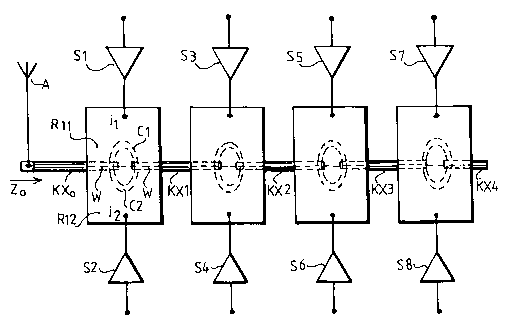
Figure 5 shows a schematic diagram of a combiner arrangement
according to the present invention, including four waveguide
resonators Rl-R4. Each resonator Rl-R4 consists of a
rectangular box as illustrated in Figure 5 (as seen from
above) and which will be further described in connection with
Figs 6 and 7.
Each resonator has the same external and internal structure.
Also the geometric dimensions of each resonator are
substantially the same, since the whole resonator assembly in
the combiner is broadband dimensioned, i.e. dimensioned for a
frequency band within certain limits, for example, 935-960
Mhz. The necessary tuning of each individual cavity
resonator due to the differing transmitter frequencies
fl,...fn is made by tuning screws, stubs etc. The channel
separation, i.e. the difference between frequencies fl,
f2,... is for example 475 KHZ.
20072~2
The cavity of each resonator, for example resonator R1
(Figure 5), is divided into two parts by means of a wall W,
to create a cavity resonator for the transmitter signals fmm
transmitter Sl (frequency fll) and a cavity resonator for the
transmitter signals from transmitter S2 (frequency f2). The
two cavity resonators within resonator R1 can be broadband
dimensioned as mentioned above.
In the center of resonator Rl, the wall W is provided with an
opening in order to give space for an output coupling
element, which consists of two clamps C1 and C2 connected
together at their ends. Clamp Cl extends into the resonator
cavity R11 and clamp C2 extends into resonator cavity R12.
Each clamp forms an output coupling loop with an electrical
length equal to a quarter wavelength. Inlets i1 and i2 to
the respective resonator cavities R11 and R12 from the
transmitters Sl and S2, respectively each consist of an
inductive loop which extends into a respective cavity in a
known manner.
The above described structure for resonator Rl is the same
for the remaining resonators R2-R4. Coaxial pieces KXO, KXl,
KX2 and KX3 connect the output coupling elements of each
resonator together and to the antenna in a serial manner.
With reference to Figure 6, the output coupling element and
the coaxial connections are shown more in detail. The two
clamps Cl and C2 are fastened at their ends to the lower
resonator wall and are bent near to the point of fastening so
as to be directed at an angle upwards from the lower
resonator wall to provide the desired degree of coupling.
When the clamps Cl and C2 are correctly directed they
together have a line impedance ZO = 50 n .
Tabs Tl and T2 at the respective points of fastening of
clamps Cl and C2 connect these to the center conductor of the
coaxial piece KXO and KXl, respectively. The two clamps Cl
_ ~ _
20a72l2
and C2 should be isolated from the wall W and from the lower
resonator wall, so that the emf induced in the loop formed by
the two clamps is coupled to the center conductor of the
coaxial line formed by the pieces KXO, KX1 and not to the
resonator walls.
As best can be seen in Figure 7, the coaxial piece KXO to the
antenna A is fastened to the lower resonator wall by means of
four screws, of which two, Bl and B2, are shown in Figure 7.
The center conductor of the coaxial piece KXO will then be
electrically connected to one shank of the clamps C1, C2.
Coaxial piece KX1 to resonator R2 is likewise fastened by
means of four screws, of which two, B3 and B4, are shown
connecting the center conductor of coaxial piece KX1 to the
other shank of clamps C1, C2. The length 1 of each clamp is
lamdaO/4 where lamdaO/4 corresponds to the center frequency
fO of the band (i.e. 935-960 Mhz).
The two clamps C1 and C2 form an output coupling element for
the electromagnetic field in the two cavity resonators Rll
and R12, respectively. Each clamp is dimensioned to have a
nominal impedance of 2Zo (= lOOn). Since the clamps are
electrically connected in parallel they together form an
impedance ZO (= 50n to the coaxial arrangement formed by the
two pieces KX0, KXl. Thus a match is obtained to the antenna
from each of the resonators Rl-R4. It is furthermore easy to
expand the number of resonators by connecting further coaxial
connection pieces to the right terminal of resonator R4.
This expansion only requires a coaxial piece having an
electrical length equal to a quarter wavelength. This in
turn implies that greater number of resonators in the
combiner can be connected to one and the same antenna.
6 -