Note: Descriptions are shown in the official language in which they were submitted.
2~7~7~
The present invention r~lates to semiconductor
photodetector devices, and more particularly to semiconductor
photodetector devices having an avalanche effect, and a
method of manufacturing them.
A so-called avalanche photocliode (hereinafter
abbreviated as an APD), wherein c:arriers are generated by
irradiating light onto a pn junction applied with a reverse
bias voltage, and are avalanche-multiplied by impact
ionization caused by the carriers, is f~atured by its
remarkable internal multiplication effect, high reæponse
characteristic, etc. Among various types of APDs, an InP-
based APD who~e light absorption layer is formed o~ either
InGaAs or InGaAsP and whose carriermultiplication layer is
formed of InP is particularly advantageous, in light of its
high quantum efficiency and low noise characteristic. This ~ :
type of InP-based APD is useful as a semiconductor
photodetector device for detecting waves in the 1 ~m band,
and constant efforts are being made to develop an improved,
practical InP-based APD.
Embodiments of the prior art and the present invention
will be described by reference to the accompanying drawings,
in which:
Fig. 1 is a sectional view showing the structure of a
conventional APD;
2~ Fig. 2 is a sectional view showing the structure of an
APD according to the first ~mbodiment of the present
invention;
:^ Figs. 3A to 3G are sectional views showing the steps for
manufacturing the APD æhown in Fig. 2;
Fig. 4 is a sectional view showing the structure o~ an
APD according to the second embodiment of the present
invention; and
;~, Figs. 5A to 5D are sectional views showing the steps for
manufacturing the APD shown in Fig. 4.
l 35
.,
..
.' i'''',,' ' ~
., .
"'-~ " ' ' . .: , ' ' , ,
20~67a
Fig. 1 is a sectional view for illustrating the
conventional APD disclosed in Published Unexamined Japanese
Patent Application No. 57-19~667. This conventional APD is
manufactured by executing a crystal growing step twice. The
manufacturing process will be briefly mentioned. ~i~st of
all, n-type InP buffer layer 52, n-type InGaAs light
absorption layer 53,
~0
- la -
2~7S70
-- 2 --
n-type InGaAsP buffer layer 54, and n~~type InP layer 55
are formed on n-type InP substrate 51 by crystal growth
in the order mentioned (the first crystal growing step).
Next, Si ions serving as n-type impurities are implanted
into a selected portion of n~-type InP layer 55, and the
resultant structure is annealed, to thereby form n~type
InP region 56. After n~-type InP layer 57 is formed on
the resultant structure by crystal growth (the second
crystal growing step), p-type region 59 serving as a
guard ring is formed by the implantation of Be ions and
subsequent annealing. ThereaEter, p+-type region 58
serving as a light-receiving region (which includes a pn
junction between n-type and p-type semiconductors and
its neighboring portions) is formed by the diffusion of
Cd. Finally, SiN film 60 serving as a reflection-
preventing film, p-type electrode 61, and n-type
electrode 62 are formed.
In general, a guard ring is formed for the
purpose of preventing an edge breakdown from occurring
in regions which are located around a light-receiving
region and in which the radius of curvature of a pn -~
junction i5 short. For this purpose, the guard ring is
made to have a graded junction, whereas the light-
receiving region is made to have an abrupt junction.
In the structure illustrated in Fig. 1/ the guard
ring fulfils its function effectively since n--type low
concentration layers 57 and 55 are located under the ~
'' ,~ ''
2~07670
guard ring so as to decrease the maximum electric field
and thereby suppress the breakdown in the guard ring
region. On the other hand, an n~type high concentration
region 56 is located under the light-receiving region so
as to increase the maximum electric field in the light-
receiving region.
To manufacture the above-mentioned structure,
crystals of InP have to be grown after the selective
ion-implantation of n type impurities and the succeeding
annealing. Normally, this crystal growth has been
performed by using a meltback technique in the liquid
phase epitaxial growth process, so as to provide a
satisfactory interface and a crystalline region. In
recent years, however, there is a tendency to manufac-
ture compound semiconductor devlces by use of a vaporphase epitaxial growth process, such as an rlocvD pro-
cess, which is superior to a liquid phase epitaxial
growth process in terms oE the controllability of
carrier concentration and film thickness. With this
tendency, more APDs have come to be manufactured by use
of the vapor phase epitaxial growth process, as long
as their manufacture requires only one crystal growing
step. In the case of the manufacture of super high-
speed APDs, the vapor phase epitaxial growth process
is indispensable.
However, if a crys-tal growing step is required
twice, as in the manufacture of the above-mentioned
. .
.
structure, and if the second crystal growing step is
performed by use of the vapor phase expitaxial growth
process, then distortion oi the lattice and precipita-
tion of impurities at the interface will be more marked
than in the case where the meltback technique is used in
the liquid phase epitaxial growth process. And in the
case of the above-mentioned structure, the interface
formed by the second epitaxial growth step will be
located in the n-side regivn of the p+n junction, as
lQ may be understood from Fig. 1. Since, therefore, a
high electric field is supplied at the interface which
is located n-side region during APD operation, a dark
current may increase and local breakdown may occur. In
addition to these problems, the above-mentioned struc-
lS ture has problems in that its guard ring is inevitably
formed in the region formed by the second crystal
growing step (which region does not have a good
crystalline condition~. These problems may also
occur where the second crystal growing step is performed
by use of the liquid phase growth process.
~ ~ .
.
2 ~ 7 ~
-- 5 --
.
In one aspect, the invention provides a semi-
conductor photodetector device which comprise~: a light
absorption layer of a fir~t-conductivity type; a window layer
~hich is of the first-conductivity type and formed o;n the
light absorption layer (the window layer is ~ormed o~ a
semiconductor whose forbidden band width is wider
than that of the semiconductor of the light absorption
layer, and ~hus allows a light of a predetermined
wavelength to pass therethrough~; a high concentration
region which is of the first-conductivity type and
located in the bottom of a depression formed in a
selected surface portion of the window layer; a re-grown
region which is of the first-conductivity type and
formed over the first-conductivity type high con-
centration region in such a manner as to fill the
depression; a guard ring which is of a second-conduc-
tivity type and formed around the depression; and a high
concentration region which is of the second-conductivity
type and formed in the window.region in such a way as to
.completely surround t.he re-grown region, the Eirst
and second-conductivity type high concentration regions
jointly providing a pn junction used as a light- :
receiving region.
In a further aspect, ~he invention provides a
method of manu~acturing a semiconductor
f.
~r ~
~7~70
-- 6 --
photodetector device, which method comprises the steps
of: growing a first-conductivity type light absorption
layer and a first-conductivity type window layer on a
first-conductivity type substrate crystal; forming
a depression in a selected surface portion of the
window layer; forming a first-conductivity type high
concentration region in the bottom of the depression
by doping first-conductivity type impurities into the ~ ~
bottom of the depression; forming a first-conductivity ~.
type re-grown region by growing a first-conductivity
type crystalline layer on the first-conducti.vity type
high concentration layer in such a way as to fill the
depression; forming a guard ring of the second-
conductivity type around the depression by doping
second-conductivity type impurities into a region ~.
located around the depression; and forming a second-
conductivity type high concentration region by doping ~
second-conductivity type impurities into the window .. ...
layer in a manner which completely surrounds the first- . ~.
conductivity type re-grown region, whereby a pn junction
used as a light-receiving region is defined between the
first and second-conductivity type nigh concentration
regions.
In the semiconductor photodetector device of .
the present invention, an interface located by the
second crystal growing step is located in the second-
conductivity type high concentration region and is not
2007670
therefore supplied with a high electric field during
the usage of the device. Therefore, the performance of
the device is not influenced by the re-grown interface
(which may not have a satisfactory crystalline
structure). Moreover, APDs which produce little dark
current and are very reliable can be manufactured with a
high yield.
In practice, it is preferable that the first and
second-conductivity types be n and p types respec-
tively, the light absorption layer be formed o:E eitherInGaAs or InGaAsP, and each of the substrate crystal,
the window layer and the re-grown layer be formed of
InP.
Normally, the above first-conductivity type
high concentration region and the guard ring are
formed by use of an impurity ion-implantation process,
and the second-conductivity type high concentration
region is formed by use of an impurity thermal diffusion
process.
Simultaneous with the above-mentioned guard ring,
a second guard ring of a second-conductivity type can
be formed such that it is located below the above guard
ring, with the first-conductivity type low-impurity
concentration layer inte:rposed~ To simultaneously
form the two guard rings, it is preferable that the
first-conductivity type impurity concentration in the
window layer be higher than that in the light absorption
' "
2~7~70
layer, and that the second-conductivity type impur~ties be
doped into the layers such that the impurity concentration
gradually decreases ~rom the surface o~ the window layer
toward the internal regions. Let it be assumed that CDx
denotes the first-conductivity type impurity concentration in
regions located between the substrate crystal and the surface
of the window layer, and CA~ denotes the doping concentration
of tha second-conductivity type impurities. In this case,
the relation CAG ~ CDx is established in the surface regions
of the window layer, the relation CAG ~ CDX is established in
regions just abvve the light absorption layer, the relation
CAG > CDx is established in the upper-most portion of the
light absorption layer and the relation CAG ~ CDx is
established in regions just above the substrate crystal.
..:
":
. ~
. ~
:
' ` ~ i
i~ '
2~7~7~
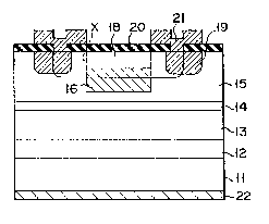
Fig . 2 is a sectional view showing an APD of the first
embodiment of the present invention, and Figs. 3A through 3G
shows the manufacturing process thereof, in order. In the
manufacturing process, n-type InP buffer layer 12, n-type
InGaAs liyht absorption layer 13, n-type InGaAsP buffer lay~r
14, and n-type InP window layer 15 are successively formed on
n-type InP substrate 11 by crystal growth (i.e. the first
crystal growing step). These layers are formed by use of the
MOCVD process in such a manner that the layers are in lattice
matching with substrate 11 (See Fig. 3A). The carrier
concentrations of layers 12, 13, 14 and 15 are approximately
5 x 1ol5 cm 3 2 x 1ol5 cm~3 1 x 1o16 cm~3 and 8 x 10¹⁵
cm 3 respectively, and the thicknesses of layers 12, 13, 14
and 15 are approximately 4 ~m, 2 ~m, 0.4 ~m, and 2 ~m,
respectively.
Next, after placing a mask on the surface of InP layer
15, a cylindrical depression having a diameter of 30 ~m~ and
a depth of 1 ~m is formed by selective etching, as is shown
in Fig. 3B. Si ions are doped into this depression, with ~n
acceleration voltage of 200 kV applied and with a dose amount
o~ 1 x 1013 cm
_ g _
.
. . .
2ao76~0
-- 10 --
maintained, as is shown in Fig. 3C. After the mask is
removed, the resultant structure is subjected to heat
treatment at a temperature of 700C. Thereafter,
n~-type InP layer 17 is formed by crystal growth (i.e.
the second crystal growing step) by use of the MOCVD
process such that the depression is filled with InP
layer 17, as is shown in Fig. 3D. As a result of the -
heat treatment, the region doped with the Si becomes
n-type high concentration region 16.
After high concentration region 16 is formed in
this fashion, an annular mask having an inner diameter
of 40 ~m~ and an outer diameter of 60 ~m~ is placed on
the region formed by the Eirst crystal growing step. In
this condition, Be ions are doped into the structure,
with an acceleration voltage of 150 kV applied and with
a dose amount of 5 x 1013 cm~2 maintained. After the
mask is removed, the structure is subjected to a heat
treatment at a temperature of 750C, to thereby form
guard ring 19, as is shown in Fig. 3E. The SiN film
deposited on the surface of the structure is patterned
out into a circular shape having a diameter of 50 ~m~,
and then Cd diffusion is performed at a temperature of
560C, to thereby form p+-type region 18 of the light-
receiving region, as is shown in Fig. 3F. At this time,
the Cd is diffused in such a manner as to completely
cover InP layer 17, so that the interface formed by the
second crystal growing step is included in p+-type
" ;, " , j ~ ; , ' ., .. ~ .~ ;. . ' ! ~
200767~
region 18. As a result, a pn junction serving as a
light-receiving region is de-Eined between n-type and
p+-type high concentration regions 16 and 18.
Finally, SiN film 20 serving as a reflection-
preventing film is formed over the light-receiving
region, and p-side electrode 21 formed by a Ti/Pt/Au
film and n-side electrode 22 formed by an AuGe/Au film
are respectively formed on the obverse and reverse
surfaces of the entire structure, as is shown in
Fig. 3G.
In the above-mentioned manufacturing process, the
doping of Be ions used for forming a guard ring may be
performed immediately after the first crystal growing
step. In this case, the formation of the depression
and the implantation of Si ions are performed after the
doping of the Be ions, and then InP crystals are grown
in such a manner as to fill the depression, with the -
ionimplanted region annealed simultaneously. If an APD
is manufactured in this fashion, the number of heat
treatments required can be reduced, and the manufac-
turing process is therefore simplified.
In the case of the conventional structure shown
in Fig. 1, interface Y formed by the second crystal
growing step is located in the n-side region of the
p+n junction and is therefore supplied with a high
electric field when -the APD is operated. In contrast,
in the case of the embodiment's structure shown in
20~76~
- 12 -
Fig. 2, interface X formed by the second crystal growing
step is located in the p+-side region, so that it is not
supplied with a high electric field when the APD is
operated. Therefore, the performance of an APD produced
by the above-mentioned manufacturing method is not
influenced by the interface which is formed by the
second crystal growing step and which may not have a
satisfactory crystalline structure. Further, the APD
; produces little dark current and is very reliable in
operation. It should be also noted that the above-
mentioned manufacturing method produces APDs with a high
manufacturing yield.
Fig. 4 is a sectional view schematically showing
the main portion of an InGaAs/InP-based APD according
to the second embodiment of the present invention.
Referring to Fig. 4, n -type InP buffer layer 31,
n~-type InGaAs light absorption layer 32, and n-type
InP layer 33 are formed on n-type InP substrate 30.
The carrier concentrations of layers 31, 32 and 33
are approximately 2 x 1015 cm~3, 2 x 1015 cm~3 and
2 x lQ16 cm~3, respectively. The thicknesses of
layers 31, 32 and 33 are approximately 4 ~m, 2 ~m and
3 ~m, respectively. In light-receiving region 38,
ion-implanted high concentration n-type region 28 and
crystal-grown n-type InP layer 29 (with which n type
region 28 is covered) are formed in a similar manner to
that of the first embodiment shown in Fig. 2. P+-type
2~1~767~
- 13 -
InP region 34 is formed in such a manner that it is 2
deep from the surface of InP layer 33 and that it
includes the interface between region 28 and layer 29.
InP region 34 provides a sharp pn junction with high
concentration n-type region 28. Around liyht-receiving
region 38, p-type guard ring 35a which is 2.5 ~m deep
from the surface of InP layer 33 and p-type guard ring
35b which extends from light absorption layer 32 to
buffer layer 31 are formed. To permit a reverse bias to
be applied to the APD, p-side contact electrode 36 and
n-side contact electrode 37 are respectively formed on
the obverse and reverse of the structure.
In the APD of the second embodiment, the guard
rings constitute a p-n-p-n thyristor construction, and a
voltage applied to the APD is distributed between the
two reverse bias junctions. Therefore, a sufficiently
high withstand voltage can be obtained with respect to
the guard rings.
Figs. 5A to 5D are sectional views showing the
steps for manufacturing the APD shown in Fig. 4.
As is shown in Fig. 5A, n~-type InP buffer layer
31, n~-type InGaAs light absorption layer 32, and
n-type InP window layer 33 are formed on n-type InP
substrate 30 in the order mentioned. Further,
ion-implanted high concentration n-type region 28 and
crystal-grown n-type InP layer 29 (with which n-type
region 28 is covered) are formed in light-receiving
2 ~7~70
- 14 -
region 38, in a similar manner to that of the first
embodiment shown in F'ig. 2. Next, as is shown in
Fig. 5B, an acceptor is doped by implanting ~Ig ions
into regions around light-receiving region 38 and
5 annealing the resultant structure, so as to form
guard rings 35a and 35b. The acceptor is doped such
that its concentration CAG is high in the surface
regions and decreases toward the deep regions. In
the meantime, the background donor concentration is
high in uppermost window layer 33, and low in both light
absorption layer 32 and buffer layer 31 (i.e., CD3 [the
donor concentration in the window layer] = 2 x 1016 cm~3;
CD2 [the donor concentration in -the light absorption
layer] = CDl [the donor concentration in the buffer
layer~ = 2 x 1015 cm~3). Therefore, the acceptor con-
centration can be controlled such that the relation
CAG > CD3 is established in the surface region (CAG >
2 x 1016 cm~3 in the case oE the second embodiment), the
relation CD3 > CAG > CD2 is established at the interface
between window layer 33 and light absorption layer 32
(2 x 1016 cm~3 > CAG > 2 x 1015 cm~3 in the case oE the
second embodiment), the relation CAG > CD2 = CDl is
established at the interEace between light absorption
layer 32 and bufEer layer 31 (CAG > 2 x 10~5 cm~3 in -the
case of the second embodiment), and the relation CAG <
CDl = CD2 is established at the interface between
buffer layer 31 and substrate 30. With the acceptor
~ 2~7~7~
- 15 -
concentration controlled in the above way, guard ring
35a which is 2.5 ~m deep from the surface of InP layer
33 and guard ring 35b which extends from light absorp-
tlon layer 32 to buffer layer 31 are formed.
Next, as is shown in Fig. 5C, Cd is difEused in a
selected portion of light-receiving region 38 such that
p+-type InP region 34 having a depth of 2 ~m is formed.
At this time, the Cd is diffused in such a manner as to
completely cover InP layer 29, so that the interface
formed by the second crystal growing step is included in
the p+-type region.
Finally, as is shown in Fig. 5D, Ti/Pt/Au
electrode 36 serving as a p-side electrode and
an AuGe/Au electrode 37 serving as an n-side
electrode are formed.
In the APD of the second embodiment, the guard
rings constitute a p-n-p-n thyristor construction, as
mentioned above. In addition, the carrier concentration
in each portion of the guard rings is as low as about
10l6 cm~3 as a result of the compensation effect acting
between the acceptor and the donor. Therefore, a high
guard ring effect is obtained in the case oE the second
embodiment.
~, ~ 25 referring to ~ erred embodiments shown in the
accompanying drawings ~ that