Note: Descriptions are shown in the official language in which they were submitted.
:~`
2~78~
The present invention relates generally to
photosensors, and more particularly to a photosensor for
detecting information on a subject such as blood pressure and
concentration of pigments in blood by transmitting light from
: 5 one side to the other side of a patient and then detecting a
. change in the magnitude of absorption of light transmitted
: through the patient's tissue.
Such an apparatus has conventionally been known for
evaluating the pulse and blood pressure by calculations made
: 10 after transmitting light through the tissue of a finger tip,
detecting a change in the transmittance (reflectance) of light
in the blood in the finger and then processing a detection
signal thereof. One example of a photosensor employed in this
apparatus is disclosed in Japanese Utility Model Laying-Open
No. 60-158803.
. The features of the prior art and the invention will
be described, by way of example, with reference to the
accompanying drawings, in which:
Figures lA and lB show one example of an arrangement
of light emitting diodes and a photodetector on a substrate
` in a first embodiment of the present invention;
~, Figure 2 is a schematic block diagram of one
embodiment of the present invention;
Figure 3 is a flow chart drawn for describing an
d 25 operation of one embodiment of the present invention;
`, Figure 4 is a timing chart for desaribing the
' operation of one embodiment of the present invention;
~ Figure 5 is a diagram showing changes in the power
! of emitted light due to a change in the temperature of the
j'. 30 light emitting diode as a~function of time;
Figure 6 is a characteristic view showing the
relationship between a current flowing through the light
~1 emitting diode and an output voltage of a photodiode;
`~ Figure 7 is a graph showing a relative light output
of the light emitting diode as a function of temperature;
Figures 8A to 8C are views showing a second
embodiment of the present invention; specifically, Figure 8A
:~ 2~7~
.
~` 2
is a plan view of the second embodiment, Figure 8B is a side
view thereof, and Figure 8C is Zl bottom view;
: Figures 9A and 9B are views showing an example in
:`. which a thermistor is provided in a heat sink of the light
emitting diode; specifically, F:igure 9A i5 a side Vi8W, and
Figure 9B is a bottom view;
Figure 10 is a schematic block diagram of a third
~ embodiment of the present invention;
; Figure 11 is a view showing one example of a
v. 10 conventional photosensor;
Figure 12 is a longitudinal section view of the
photosensor shown in Figure 11;
Figure 13 is a cross sectional view in which the
photosensor of Figure 10 is attached to a finger; and
Figure 14 is a perspective view of an attachment
tape for securing the photosensor to a finger.
~: Figure 11 is a perspective view of a conventional
photosensor disclosed in the above Japanese Utility Model
` publication; Figure 12 is a cross sectional view of the
" 20 photosensor shown in Figure 11; Figure 13 is a cross sectional
view showing the photosensor of Figure 11 attached to a
`~; finger; and Figure 14 is a perspective view of a fixing tape
for securing the photosensor onto a finger.
First, a conventional photosensor 8 will now be
~ 25 described with reference to Figures 11-14. The photosensor
`~ 8 shown in Figure 11 transmits light from one side to the
other side of the finger and detects a change in the magnitude
of this transmitted light depending on the blood content in
I the finger. A light emitting element 2 and a light receiving
3 30 element 3 are spaced a predetermined distance, corresponding
to the size of the finger, apart from each other on a flexible
film substrate 1. A transparent flexible light transmissive
film 6 is attached to the film substrate 1 so as to cover the
~ light emitting and receiving elements 2 and 3.
., 35 The usage of the photosensor 8 shown in Figure 11
j will be described with re~erence to Figures 12-14. The
2~778'~
.
photosensor 8 is wound around a finger 7 so that the tip of
the finger 7 is sandwiched between the light emitting element
2 and the light receiving element 3, as shown in Figure 12.
The fixing tape 9 shown in Figurs 14 is then wound on the
photosensor 8 and around the ~inger. This fixing tape 9 is
; rectangular and comprises physical adhesion means on a front
surface of its one end and on a reverse surface of the other
end. Winding this tape 9 on the photosensor 8 to lap the
front surface of one end over the reverse surface of the other
end causes the photosensor 8 to be firmly secured onto the
finger 7. When a power is supplied to conductors 4 through
~ a connector 5 of a signal processing apparatus (not shown),
,~ the light emitting element 2 emits light. This emitted light
- is transmitted through the finger 7 and directed to the light
receiving element 3. The light receiving element 3 receives
this light and supplies a detection signal to the main body
of the signal processing apparatus through the lead 4 and the
connector 5. The signal processing apparatus detects a change
in the transmittance at this time, processing the detected
signal and then performing a calculation to provide a pulse
and a blood pressure value.
The light emitting element 2 employed in the above
photosensor 8 generally uses a light emitting diode. ~he
light emitting diode is liable to have its output power and
the wavelength of emitted light change depending on ambient
temperature. In addition, attaching the photosensor 8 onto
a living body, e.g. the finger 7 renders the living body
ischemic or hemostatic, so that the body temperature of the
finger 7 ls decreased, or increased due to an increase in
blood pressure. Thus, the ambient temperature of the light
emitting element 2 changes, and consequently the output power
or the luminescence wavelength change. However, the output
power or the luminescence wavelength of the light emitting
- element 2 is required to be kept constant in order to
`~ 35 correctly measure a pulse value, a blood pressure value and
the like.
,............................................................................ .
-:
'I .
2~7~8~
; It is an object of the present invention to provide
a light absorption detector referred to herein simply as
photosensor in which an output power or wavelength of a light
emitting element does not changeleven with a change in ambient
temperature.
It is another object of the pxesent invention to
provide a photosensor for detecting a change in the quantity
; of light with a change in the temperature of a light emitting
element, controlling current flowing through the light
emitting element in response to a detected output thereof and
correcting the change in the quantity of light with the change
in the temperature of the light emitting element.
It is a further object of the present invention to
provide a photosensor in which an output pover or wavelength
does not change with a light emitting element or ambient
;I temperature of the light emitting element being kept constant,
even if the photosensor is attached to a subject.
Briefly, the photosensor or light absorption
` detector according to the present invention emits light to a
subject, receives light from the subject and detects the
magnitude of absorption of light by the subject. In this
photosen~or, a light emitting element which directs light to
the subject is provided on a film substrate; a first light
receiving element is spaced, on the film substrate, a
~ 25 predetermined distance apart from the light emitting element;
;'l and a second light receiving element is provided near the
light emitting element. Current flowing through the light
emitting element is controlled so as to correct a change in
the quantity oE light with a change in the temperature of the
light emitting element in response to the power of received
~ light of the second light receiving element.
3 Therefore, in accordance with the present invention,
the light emit:ting element or the temperature of the light
emitting element can be kept constant independently of a
change in the temperature of the subject. This enables the
output power or wavelength of the light emitting element to
r~
; 2~7~8~
be kept constant, thereby obtaining correct information on the
subject.
According to another aspect o~ the present
; invention, a heater and a temperature sensor are provided near
at least either one of the light emitting element and the
light receiving element, and the vicinity of either the light
emitting or the light receiving element is heated by such a
heater so that a detected temperature is maintained constant.
Therefore, also in this aspect, the temperature of
the light emitting element or the light receiving element can
be kept constant independently of the subject's changing
temperature so that the output power or wavelength of the
light emitting element is kept constant, and thus correct
subject information is obtained.
The foregoing and other objects, features, aspects
and adva~tages of the present invention will become more
apparent from the following detailed description of the
present invention when taken in conjunction with the
accompanying drawings.
~`l 20 Figure lA is a plan view of one example of light
i emitting diodes and a photodetector in one arrangement of an
embodiment of the present invention, and Figure lB is a side
view thereof. Referring to Figures lA and lB, a light
; emitting diode 10 substitutes for the light emitting element
2 of the conventional photosensor 8 shown in Figure 10. Two
LED chips LEDI and LED2 are provided on a substra~e 12, and a
photodiode PD is provided near these LED chips LEDI and LED2.
The photodiode PD directly receives light from the LED chips
LEDI and LED2. The LED chips LEDI and LED2 usually radiate
light also to portions beneath a p-n junction plane, and this
~, radiated light is received by the photodiode PD acting as a
photodetector.
The photodiode PD detects a change in the quantity
of light from the LED chips LEDI and LED2 in accordance with
a change in the ambient temperature. Transparent epoxy resin
13 is applied onto the substrate 12 so as to cover these LED
,j
' '.i' '' " ' ~ ' . ", ' , , ` ' ' ' ~ '
2~7~
chips LEDI and LED2 and the photodiode PD. The epoxy resin may
~ be replaced by transparent polyester resin. The photodiode
; PD may be provided at a position where light radiated from the
LED chips LEDI and L~D2 can reflect on an inner surface of the
semi spherical epoxy resin 13 to be received by the photodiode
: PD. Further, the following process may be employed as shown
in Figure lB. An Ag film 131 on which Ag is evaporated is
formed on a portion of the surface of the epoxy resin 13. The
~ light radiated from the LED chips LEDI and LED2 i5 then
; 10 positively and partially reflected at the Ag film 131, and
` this reflected light is detected by the photodiode PD.
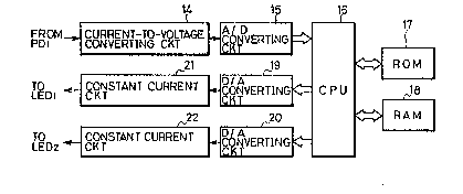
Figure 2 is a schematic block diagram of the first
. embodiment of the present invention. Referring to Figure 2,
;`~ power generated by light received by the photodiode PD shown
: 15 in Figures lA and lB, is supplied to a current-to-voltage
converting circuit 14. Current flowing through the photodiode
PD is then converted into voltage, and this voltage is
~;~ supplied to an A/D converting circuit 14. An A/D converting
~;. circuit 15 converts a voltage value into a digital value and
l 20 then supplies the digital value to a CPU 16. The CPU 16 is
il connected to a ROM 17 and a RAM 18. As shown in Figure 3
which will be described later, a program for correcting the
. change in the quantity of light of the LED chips LED~ and LED
with the change in temperature, has been stored in the ROM 17.
The CPU 16 supplies a current value flowing through the LED
. chips LED~ and LED2, as a digital signal, to D/A converting
circuits 19 and 20. The D/A converting circuits 19 and 20
convert a digital value ajs the current value into an analog
~ value and supply this analog value to constant current
i 30 circuits 21 and 22. The constant current circuit 21 supplies
a current to the LED chip LED~, while the constant current
circuit 22 supplies a current to the LED chip LED2.
Figure 3 is a flow chart drawn for the description
of a detailed operation of one embodiment of the present
l 35 invention; Figure 4 is a timing chart therefor; Figure 5 shows
.` a change in the power of emitted light of the light emitting
. ~
.,
2~7~
,.
diode due to a change in the temperature thereof; Figure 6 is
a characteristic diagram showinq the relationship between a
current flowing through the light emitting diode and an output
voltage of the photodiode; and Figure 7 shows a relative light
output as a function of temperature characteristic of the
light emitting diodes LED~ and LE~2.
Referring to Figures lA-7, the detailed operation
of one embodiment of the present invention will now be
described. Since each of the LED chips LEDI and LED2 operate
in a similar manner, only the operation of the LED chip LED~
will be described. An output current ipDIp of the photodiode
PD receiving light shown in Figure 4(a) is supplied to the
current-to-voltage converting circuit 14 to be converted into
a voltage VPD~P~ as shown in Figure 4 (b). This converted
voltage is then further converted into a digital signal by the
A/D converting circuit 15 which supplies the dig~tal signal
to the CPU 16. The CPU 16 samples the output voltage VPDIP of
the photodiode PD to determine if this output voltage VrD~p is
lower than a predetermined output voltage Vl of the photodiode
PD and lower than allowable voltage ~V~ thereof. If the
output voltage VPDIP is determined as VPDIP > Vl + ~VI, the CPU
16 increas~s or decreases a value of a current iL~DI flowing
through the LED chip LEDI.
In this case, the relationship of VPDIP =a~iL~Ip at a
specific temperature may be obtained with respect to the
characteristic of VPDIP as a function of iL~Ip shown in Figure
,~ 6 to increase or decrease the value of the current iL~I by the
.! value of ¦ VPDIP -V¦/a. The specific temperature in this case
is preferably selected in the range of 35C-38C close to the
~ 30 body temperature of a human body.
`r In general, the power of emitted light of the light
emitting diode 10 increases with a decreasing temperature or
decreases with an increasing temperature, as shown in Figure
7. Thus, when the temperature decreases as shown in Figure
5 (a), the power of emitted light of the light emitting diode
10 increases as shown in Figure 5 (b). However, decreasing
,i .
" ' id'`
.'.
~'" ;,: '' ' . ` ' ' ' ~ ` , :
2~77~ll
:.
a supply current i of the light emitting diode 10 to offset
this increased amount of the emitted light power (Figure 5(c))
enables the emitted light power to approximately be constant
and thus enables a correction of a fluctuation in the emitted
light power with a change in the temperature, as shown in
Figure 5 (d) as a function of time.
Figures 8A to 8C show another embodiment of the
present invention; specificallyl Figure 8A is a plan view,
Figure 8B is a side view and Figure 8C is a bottom view.
lo The construction of this embodiment of the present
invention will now be described with reference to Figures 8A
i to 8C. A photodiode 31 as one example of the light receiving
element is provided at one end of the surface of a film
` substrate 30. Lead terminals of the photodiode 31 are
~,! 15 soldered onto patterns 32 formed on the film substrate 30.
~ A light emitting diode 34 as one example of the light emitting
¦ element is provided at the other end of the surface of the
, film substrate 30. Lead terminals of the light emitting diode
;~ 34 are soldered onto patterns 35 formed on the film substrate
30. A thermistor 37 as one example of temperature detecting
means is provided near the light emitting diode 34. Patterns
~; 33, 36 and 38 for connecting cables are formed on the left
side of the pattern 35. The patterns 33 and the patterns 32
are for the photodiode 31, the patterns 36 and the patterns
35 are for the light emitting diode 34, and the patterns 38
are for the thermistor 37. The patterns are electrically
`! connected through linear conductors as shown.
A heater 39 as one examplè of heating means is
`l provided at a position, corresponding to the light emitting
i 30 diode 34, on the reverse surface of the film substrate 30.
This heater 39 comprises a nichrome (trademark) resistor
i thinly formed, for example. Terminals of the heater 39 are
`~ electrically connected to patterns 40.
In the photosensor constructed as above, a main body
of a processing apparatus shown in Figure 10, which will be
described later, is connected through a cable (not shown) to
. ; .
.~
2~ 3778
ll 9
the patterns 36 for the light emitting diode 34, the patterns
38 for the thermistor 37, the patterns 33 for the photodiode
31 and the patterns 40 for the heater 39.
, Figures 9A and 9B show an example in which the
3 5 thermistor 37 is located in a heat sink 341 of the light
emitting diode 34. Terminals 34~ for the light emitting diode
34 and terminals 343 for the thermistor 37 are attached to the
. heat sink 341.
While the above embodiment shows the example in
~: 10 which the thermistor 37 is provided near the light emitting -
diode 34, the thermistor 37 and the heater 39 may be located
near the photodiode 31, as shown by the dotted line of Figure
8B, in relation to ambient temperature of the photodiode 31.
Figure 10 is a schematic block diagram for
illustrating the operation of ~he detector according to the
above described second embodiment of the present invention.
A temperature detecting signal of the thermistor 37 shown in
~ Figure 8A is applied to a current-to-voltage converting
.~ circuit 41 for conversion into a voltage which is further
,, 20 converted into a digital signal by an A/D converting circuit
42 the output of which is applied to a CPU 43. The CPU 43 is
connected to a ROM 44 and RAM 45, The ROM 44 has stored ~.
;`~ therein a program for controlling the heater 39 in response
,~ to a temperature detected by the thermistor 37 so that the
l 25 ambient temperature of the light emitting diode 34 shown in
j Figure 8A is maintained constant. The RAM 45 stores data of
the temperature detected by the thermistor 37. The CPU 43
supplies data of a current, which is to flow through the
heater 39, to a D/A converting circuit 46 in response to the
digital signal representing the detected temperature, which
is supplied ~rom the A/D converting circuit 42, in accordance
with the program stored in the ROM 44. The D/A converting
`~ circuit 46 converts the digital signal into an analog signal,
so that a current is supplied from a constant current circuit
~ 35 47 to the heater 39.
,' , .
~ ;.s
.'~ .
.~
2~77~
:
As has been described above, according to this
embodiment, since the thermistor 37 and the heater 39 are
located near at least either one of the light emitting diode
34 and the photodiode 31 so that the vicinity of at least one
of the light emitting diode 34 and the photodiode 31 is heated
by the heater 37 to make the detected temperature constant,
the temperature of the light emitting diode 34 or that of the
photodiode 31 is kept constant independently of the change in
. the temperature of the subject. Consequently, it becomes
possible to keep the output power and wavelength of the light
emitting element constant and thus obtain correct subject
information.
Although the present invention has been described
and illustrated in detail, it is clearly understood that the
same is by way of illustration and example only and is not to
be taken by way of limitation, the spirit and scope of the
present invention being limited only by the terms of the
appended claims.
~ I .
`i :: :
, :
:~,
}
s
. .
.
,..
$
:~,