Note: Descriptions are shown in the official language in which they were submitted.
` c~ ~o~y
2C~7952
S P E C I F I CAT I ON
:.
Title of the Invention
PIEZOELECTRIC ELEMENT WITH GIANT ELECTROSTRICTIVE EFFECT AND
CERAMIC COMPOSITION FOR PREPARING SAME
. .
.
sackqround of the Invention
a) Field of the Invention
The present invention relates to a longitudinally effective
piezoelectric element. More particularly, it relates to a
longitudinally effective piezoelectric element exhibiting a giant
- displacement at low voltage and to a ceramic composition suitable for
. .7
producing the longitudinally effective piezoelectric element.
Such type of longitudinally effective piezoelectric element is
; practically applied to a wire driving element of impact dot matrix
printers, a positioning element of super precision main table for use
in the production of semiconductors and other various elements. It
is now expected to further develop in the future for accurate
.,
positioning elements and micro driving elements.
:
'1 ' '
b) Prior Art of the Invention
Conventionally, typical actuators are motors driven by
electromagnetic force, systems converting rotation of electromagnetic
motors to a linear motion through combination of gears or voice coils
.7, ~.
obtained by combining electromagnetic coils with springs. These
~ actuators are widely used in machinery for high speed continuous
'':'3'', rotation and positioning.
:::
... .
. ..,~
" .: : .
.$ ` . . : -
Z~3~7952
Recently, the demand for new actuators has rapidly increased
mainly in the field of optical precision instruments and semiconductor
elements. For example, the demand is in the working of optical
instruments such as lasers and cameras, in the positioning of
semiconductor production equipment, and in the adjustment of optical-
pass length in optics and astronomy. The required precision has
already reached to a level of 1 micron or less and the requirement
for precision will become increasingly severe. In order to satisfy
these requirements, conventional positioning devices utilizing
electromagnetic motors are too complex in construction and
controlling, and voice coils have also disadvantages in output and
response.
General characteristics required for a novel actuator in place
of the above conventional actuators are summarized as follows.
1. Large displacement,
2. No or small hysterisis error,
3. Quick responsivility,
4. Driving ability under low energy,
5. Large output,
6. Slight influence by temperature variation,
7. Small size and light weight,
8. No deterioration during use.
Recently, attention has been rapidly focused on an
electrostrictive actuator utilizing piezoelectric and/or
electrostrictive properties of ceramics as a candidate for the novel
actuator satisfying the above requirements.
The electrostrictive property sometimes includes, in a broad
~,
~ - 2 -
... .
x
. ..
. ~ . . - . . .
,,......... :, . .. . .
,,. - . , : . :.. ,, : . .
: . , : : - .. , , :
, : : ,, ~ -
20~79~2
.
sense, a piezoelectric property in that ceramics generate strain when
an electric field is applied to the ceramics. However, in a narrow
sense, the electrostrictive property is defined as a propert-y where
the strain factor is proportional to the square of electric field
strength. On the other hand, the piezoelectric property is defined as
a property where the strain factor is proportional in a first order
to electric field strength. Further, the ceramics having a
piezoelectric property causes spontaneous polarization and hence
. exhibits a very high coercive field and polarization treatment must be' 10 carried out in order to use it for elements. The present invention
- defines the piezoelectric material having a coercive field in excess
~ of 5 kV/cm as a hard material. On the other hand, the ceramics having
..
an electrostrictive property have a coercive field of 0 kV/cm and
causes no spontaneous polarization. Consequently, no polarization
treatment is required. The present invention defines the ceramics as
an electrostrictive material. In addition, an intermediate
piezoelectric material between the hard material and the
electrostrictive material, practically a piezoelectric material
having a coercive field of approximately from 0 to 5 kVtcm, easily
changes its direction of polarization depending upon the applied
~ electric field. Such type of piezoelectric material has also no
j requirement for polarization treatment. The present invention defines
;~ such type of piezoelectric material as a soft material.
Reference is made in the following description to various Figures of the
accompanying drawings which, eor the sake of convenience, are first briefly introduced
~1 below:
. - 3 -
...... ..
ix:
.... , : .. -.. ;. .-:.^
", .. ,, . .: : : ;:
~ 20079~2
Figure 1(a), Figure 1(b) and Figure 1(c) are electric field-strain cuuves of an
electrostricthe material, a hard material and a soft material, respectively.
In Figures l(a), 1(b) and 1(c), A indicates a displacement amount ~ I/l at a
coerche field of 10 IcV/cm, and B indicates a coercive field.
Fgure 2 is a multilayered type longitudinally effective piezoelectric element having
an internal electrode plate which covers a portion of the element section. In Figure 2,
1 indicates a ceramic composition, 2 indicates an external electrode and 3 indicates an
' internal electrode and 4 indicates a lead wire.
Figure 3(a) is a multilayered type longitudinally effective piezoelectric element
having an internal electrocb plate which covers the whole section of the element. In the
Figure, an external electrode and a lead wire are omitted for the purpose of simplicity.
:~ In the Figure, S indicates a ceramic composition, 6 indicates an insulation layer and 7
indicates an internal electrode. Example 38 has 51 sheets of ceramic composition 5 in the
laminated layer.
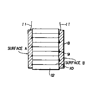
Figure 3(b) is a multilayered type longitudinally effecthe piezoelectric elementhaving an internal electrode plate which covers the whob section of the element. Figure
3(b) is a drawing of sections vertically cut on surface (A) and surface (B) in Figure 3(a).
In the drawing, 8 indicates an external electrode, 9 indicates an insulation layer, 10
indicates an internal electrode, 11 indicates a lead wire and 12 indicates a ceramic
2 0 composition.
-. Fgure 4 is a single plate of a longitudinally effective piezoelectric element.
. In the drawing, 13 indicates a ceramic composition and 14 indicates an electrode and lS
indicates a pair of lead wire.
" 1
As mentioned above, the electrostrictive material is roughly classified into three
:::
groups, that is, (1) a hard material, (2) a soft material and (3) an electrostrictive material.
~ Representathe examples of electric field-strain curves of these materials are
.
:.;
.; _
.:, . -. , - ~ .
, . . . . .
:: . -. .,: . , s.,
: . . ~ :
illustrated in Figures l(a), l(b) and l(c). 2~7952
As illustrated in the electric field-strain curves of Figures
l(a), l(b) and l(c), in the cases where the electric field is
alternately applied to these materials, the samples initially cause
shrinkage in appearance due to their residual polarization as
compared with the state thereof in the electric field level of 0
kV/cm and then lead to a rapid expansion. The coercive field of the
present invention is defined as a value of the electric field where
the rapid expansion starts. The strain factor is a value represented
by the displacement amount ( ~ ~ ) and the length (~ ) of a sample in
the direction of applied electric field when an electric field of 10
kV/cm is applied to the sample. The strain factor is indicated by
,,,
X 100 (%).
At present a generally known electrostrictive material is:
'~ pb(Mgl/3Nb2/3 )O~
and further includes ceramics based on:
(Pb,sa)(Zr,Ti)03
(hereinafter abbreviated as PBZT).
As to PBZT ceramics, K.M. Leung et al of HANEY WELL C0. already
:.3 reported on a composition:
}~ (Pbo 73Bao 27)o. o7BiO. o~ZrO. 70Tio. 300
~Ferroelectric, vol 27, page 41-43(1980) ~ .
According to the report, the composition had an electro-
strictive property and a coercive field of 0 kV/cm. Even though an
electric field of 10 kV/cm was applied to them, the ceramics of the
above composition exhibited a strain factor of only 0.06 ~. The
present inventors also confirmed the same result in the below
:3,
:- . . . , : ' . ,
2C`~9S2
described Example 40. According to the investigation of this
inventors, the dielectoric permittivity is from 5000 to 6000.
The ceramics of such composition require high voltage in order
to obtain a large displacement, also have a disadvantage of a large
electrical consumption due to their high dielectric permittivity
during drive in high-frequency electric field and hence are quite
difficult to be used for actuators. Further, the ceramics of such
composition exert a marked weight loss in a sintering process. The
weight loss amounts to 10 %. The weight loss is assumed to depended
on lead evaporation which causes severe problems in the industrial
production.
On the other hand, Japanese Patent Laid-Open Publication 60-
144984(1985) discloses a ceramic composition on the basis of
PBZT + Pb-Ba-Bi-W where the content of W+ Bi is 1.5 atom % or less.
The composition can be applied to actuators utilizing a transverse
piezoelectric effect.
The transverse piezoelectric effect refers to the effect
utilizing displacement in the rectangular direction to the direction
of applied electric field. The effect is used, for example, for
bi-morph elements etc. On the other hand, the longitudinal
piezoelectric effect refers to the effect utilizing displacement
parallel to the direction of applied electric field. The effect is
used for multilayered piezoelectric elements etc. as illustrated in
the present invention. The ceramic composition disclosed in Japanese
Patent Laid-Open Publication 60-144984(1985) is a hard material
having a coercive field of exceeding 5 kV/cm. The composition must
be subjected to polarization treatment prior to use as illustrated in
:;
.:~
~ - 5 -
. . .
. .,
"
20~7952
the examples of the publication. As illustrated in Examples 41 and
42 described below, the ceramic composition exhibits a strain factor
of only 0.08 ~ even in the electric field of 10 kV/cm, and cannot be
employed at all for the elements exerting 2 large displacement.
Many patents have been applied for ceramic compositions
containing PBZT and various metal dopants. Several patents have also
been applied for ceramic compositions containing alkali metals and/or
alkali earth metals in place of lead. Any of these compositions,
however, is used for elements or filters having a high dielectric
permittivity and not characterized by a large displacement.
As to the longitudinally effective electrostrictive element, a
multilayered type longitudinally effective piezoelectric element is
marketed from NEC Corp. According to the catalog thereof, the element
has a coercive field of 6 kV/cm. The strain factor is 0.09 % at an
applied electric field of 15 kV/cm and about 0.06 ~ at an applied
electric field of 10 kV/cm. These displacements are considerably
small and hence a complex displacement magnifying mechanism or a high
voltage generator is required. The element still has many
disadvantages to be improved.
Other longitudinally effective electrostrictive elements have
also been reported in papers etc. However, any of these elements has
a similar strain factor to that of the above NEC's element.
As mentioned above, the longitudinally effective piezoelectric
element having a large displacement has not yet been fully developed.
SummarY of the Invention
One object of this invention is to provide a longitudinally
- 6 -
,
s, , , . ~ ., . ,, . - .. ,
:. :
: ' '' ' ,, . , -, ' . :,
, ~, - , , . ., ~,;
",
,- . ..
2C$79S2
effective piezoelectric element having a large strain factor, a
multilayered type longitudinally effective piezoelectric element and
a soft material for use in making the elements.
The present inventors have carried out an intesive
investigation in order to achieve the above object. As a result, the
following information has been obtained. A hard material having a
coercive field of more than 5 kV/cm and an electrostrictive material
having a coercive field of 0 kV/cm cannot provide an element having a
large displacement. Only a soft material having a coercive field of 0
to 5 kVlcm can provide the longitudinally effective piezoelectric
element having a large displacement. In order to obtain the soft
material, it is also important to optimize the kind of PBZT
composition and the amount of dopants. Further, the longitudinally
effective piezoelectric element exhibiting a very large strain factor
can be obtained by utilizing an electrostrictive ceramic composition
having a coercive field of 0 to 5 kV/cm, preferably 1 to 4 kV/cm.
One aspect of this invention is a piezoelectric element
i .,~
exhibiting a giant displacement which essentially comprises providing
an electrode on both sides of a thin plate or thin film of a ceramic
composition represented by formula (I ):
(Pb~ sa~-x). Me~(ZrJ Til-J)c O~ ( I
~:`
wherein x, y, a, b and c are a value having a range of 0.70<x<0.80,
0.455 y5 0.65, 0.855 aS l.lS, 0.0015 b~ 0.1 and 0.855 cS 1.15,
`;~ respectively; d is a value determined by the oxidized state of each
element; and Me is one or more of metals selected from the group
consisting of Ta, Nb, Nd, Y, Th, Bi and W, and exhibiting an
j electrostrictive property having a coercive field in the range of from
;~
;. .
2G~7952
....
higher than 0 kV/cm to 5 kV/cm or less.
Another aspect of this invention is a piezoelectric element
exhibiting a giant displacement having a ceramic composition
represented by formula (I ) wherein x, y, a, b and c are a value
having a range of 0.70<x<0.75, 0.45~ y5 0.65,
0.85~ a~ 1.15, 0.001S b~ 0.06 and 0.855 c5 1.15, respectively; d
is a value determined by the oxidized state of each element; and Me is
i one or more of metals selected from the group consisting of Ta, Nb,
Nd, Y, Th, si and W.
S Further aspect of this invention is a piezoelectric element
exhibiting a giant displacement having a ceramic composition
represented by formula (I ) wherein x, y, a, b and c are a value
having a range ofO.755 x<0.80, 0.455 yS 0.65, 0.85~ a~ 1.15,
0.02~ b~ 0.01 and 0.85 ~ c~ 1.15, respectively; d is a value
determined by the oxidized state of each element; and Me is one or
~;~ more of metals selected from the group consisting of Ta, Nb, Nd, Y,
Th, Bi and W.
: ~ .
Still another aspect of this invention is a multilayered
piezoelectric element exhibiting a giant displacement which
essentially comprises alternately stacking an electrode plate and a
ceramic composition represented by formula (I ) wherein x, y, a, b and
c are a value having a range of 0.70<x<0.80, 0.455 yS 0.65,
0.855 a~ 1.15, 0.0015 bS 0.1 and 0.855 cS 1.15, respectively; d is
a value determined by the oxidized state of each element; and Me is
one or more of metals selected from the group consisting of Ta, Nb,
Nd, Y, Th, Bi and W, and exhibiting an electrostrictive property
having a coercive field in the range of from higher than 0 kVicm to 5
:~ - 8 -
,.,.,.~
..... .
.. ., ~ . . ..
.
, ..... . ..
.
~. . .. ~
.~~
XG~7952
kV/cm or less, and further providing an external electrode.
Still further aspect of this invention is a multilayered
piezoelectric element exhibiting a giant displacement having a ceramic
composition represented by formula ( I ) wherein x, y, a, b and c are
a value having a range of 0.70<x<0.75, 0.45~ y~ 0.65,
0.85~ aS 1.15, 0.001~ b~ 0/06 and 0.85~ c~ 1.15, respectively; d
is a value determined by the oxidized state of each element; and Me is
one or more of metals selected from the group consisting of Ta, Nb,
Nd, Y, Th, Bi and W.
Another aspect of this invention is a multilayered
piezoelectric element exhibiting a giant displacement having a
composition represented by formula ( I ) wherein x, y, a, b and c are
a value having a range of 0.75~ x<0.80, 0.45~ y~ 0.65,
0.85~ a~ 1.15, 0.02~ b~ 0.1 and 0.85~ c~ 1.15t respectively; d is
a value determined by the oxidized state of each element; and Me is
one or more of metals selected from the group consisting of Ta, Nb,
Nd, Y, Th, Bi and W.
Further aspect of this invention is a piezoelectric ceramic
composition exhibiting a giant piezoelectric effect represented by
formula ( I ) wherein x, y, a, b and c are a value having a range of
0.70<x<0.80, 0.45~ y~ 0.65, 0.85~ a~ 1.15, 0.001~ b~ 0.1 and
0.85~ c~ 1.15, respectively; d is a value determined by the oxidized
state of each element; and Me is one or more of metals selected from
the group consisting of Ta, Nb, Nd, Y, Th, Bi and W.
Still another aspect of this invention is a piezoelectric
ceramic composition exhibiting a giant piezoelectric effect
represented by formula ( I ) wherein x, y, a, b and c are a value
_ g _
.
2~79~2
,:
having a range of 0.70<x<0.75, 0.45~ y~ 0.65, 0.85~ a~ 1.15,
O.OOlS b~ 0.06 and 0.85~ c~ 1.15, respectively; d is a value
determined by the oxidized state of each element; and Me is one or
more of metals selected from the group consisting of Ta, Nb, Nd, Y,
i. Th, Bi and W.
Still further aspect of this invention is a piezoelectric
ceramic composition exhibiting a giant piezoelectric effect
represented by formula ( I ) wherein x, y, a, b and c are a value
: having a range of 0.75 ~ x<0.8, 0.455 y~ 0.65, 0.85S a5 1-15,
0.02~ b~ 0.1 and 0.85~ c~ 1.15, respectively; d is a value
determined by the oxidized state of each element; and Me is one or
.:. more of metals selected from the group consisting of Ta, Nb, Nd, Y,
, ....
Th, Bi and W.
,~ .
,~
~, ,
~,
s~
1 0 --
~',' .
~ . . .
.': ', , ' ' ` .
,'1', ` ' . ' ' ' ' : ''
,',. ' ' ~ ` , .
.',', ' ' ' ' ' ' ` ' .
, . . .
20079~2
~ .5
Detailed Description of the Invention
In the practice of this invention, the PBZT skeleton
composition is important. In the above formula (I ), x, y, a and c
are a value in the range of 0.70<x<0.80, 0.45 ~ y~ 0.65,
0.85~ aS 1.15 and 0.85~ cS 1.15, respectively. When the value of x
is smaller than 0.70, the value of y is larger than 0.65, or the
value of a is smaller than 0.85 or larger than 1.15, or when the value
of c is smaller than 0.85 or larger than 1.15, the composition is an
electrostrictive material and unsuitable for use because the coercive
.~
' 't
. .,
~ A,
~'
.-.; .
20~379S2
, . . .
field becomes 0 kV/cm and strain also lowers. On the other hand, in
the cases where the value of x is larger than 0.80 or the value of y
is smaller than 0.45, the composition is a hard material and the
, .
coercive field exceeds 5 kV/cm. The composition requires
polarization treatment, gives a small strain and hence is also
unsuitable for use.
In the present invention, one or more of elements selected from
the group consisting of Th, Ta, Nb, Nd, Y, si and W must be added to
the psET skeleton composition as a dopant, that is, Me in the above
formula (I ).
Patents which comprise addition of A~ 2 03 have been applied.
However, addition of elements other than those found by the
present inventors has no effect on the magnification of strain. As
illustrated in Examples 43 and 44 described below, metals such as
aluminum and iron give adverse effects because these metals
remarkably increase thier coercive field and decrease strain.
When the values of x, y, a and c in the PBZT skelton
composition of the above formula (I ) are in the range of 0.70<x<0.80,
0.45~ y~ 0.65, 0.85~ a~ 1.15 and 0.85~ c~ 1.15, respectively,
the amount of dopants is in the range of 0.001~ b~ 0.10. When the
value of b exceeds 0.10, the ceramic composition becomes an
electrostrictive material and is unsuitable for use because the
coercive field is 0 kV/cm and strain decreases remarkably. On the
other hand, in the case where the value of b is smaller than 0.001,
the ceramic composition exhibits a hard piezoelectric property having
a coercive field of exceeding 5 kV/cm and is also unsuitable for use
due to its decrease in strain.
. .
- l 2 -
: ., . , '
,,. ~ ' . . . .
~: ' . , , :... ,
:: .
~., :~. .. . .
.;.;. ^ ' . '
` ZG~79~2
:,
.
A preferred range of b is 0.001 ~ b~ 0.06 when the ranges of
x, y, a and c are 0.70<x<0.75, 0.45 ~ y~ 0.65, 0.85~ a~ 1.15 and
0.85~ c~ 1.15, respectively. Another preferred range of b is 0.02
b~ 0.10 when the ranges of x, y, a and c are 0.75~ x<0.80,
0.45~ y~ 0.65, 0.85~ a~ 1.15 and 0.85~ c~ 1.15, respectively.
The structure of a multilayered type longitudinally effective
piezoelectric element exhibiting a giant displacement of this
invention is illustrated in Figures 3(a) and 3(b). Films or thin
plates of ceramic composition obtained by this invention and internal
electrode plates are alternately multilayered. The internal
electrode plates are wired so as to have a plus or minus pole
alternately every layer and equipped with lead wires and external
connection terminals in order to couple with external circuits. The
size of the element is arbitrary and specified by the system where
the element is integrated. The thickness of film or thin plate of the
ceramic composition is also arbitrary. However, a thinner film or
plate is preferred for preparing an element exhibiting a large
displacement at low voltage. Hence, the thickness of the ceramic
composition is usually 2000 ~ m or less, preferably 500 ~ m or less
and more preferably 200 ~ m or less. On the other hand, when the
ceramic composition becomes too thin, unfavorable effects are
observed, for example, cracks are liable to generate during operation
and poor insulation occurs between electrodes. Accordingly, the
thickness of the ceramic composition is preferably 1 ~ m or more,
more preferably 3 ~ m or more and most preferably 6 ~ m or more.
Materials of the internal electrode plates are usually gold,
silver, palladium, platinum, copper, nickel etc. and alloys of these
- 1 3-
.~
.
: . -
~` . ..
,
.. : . .: i . . . ,.. , . ~: . ..
.;, -, ,, ` , .. . .
, , ., -. . . ...
. .. ...
, .
2CJ~79S2
metals. As illustrated in Figure 2, the internal electrode plate may
cover merely a portion of the section of the element. In this case,
however, stress is concentrated around the edge of the electrode plate
during operation and sometimes causes destruction. Consequently, it
is preferred to cover the whole section of the element with the
internal electrode plate.
The multilayer numbers of the internal electrode plate and the
film or thin plate of the above ceramic composition is arbitrary. The
.
multilayer number may be one, that is, a single plate. Various ways
of multilayering are admitted. Ceramic compositions having different
kinds of thickness may be multilayered and those containing different
components may also be multilayered. The latter case, in particular,
is advantageous in that properties other than displacement of the
element, for example, dielectric permittivity , tan ~ and temperature
dependency, etc. can be varied to meet the requirements of the system
where the element is integrated.
The element of this invention is sometimes sealed in order to
protect a jointing portion of the internal electrode plate and the
lead wire or the external connection terminal. The preferred sealing
material is a flexible resin. Sealing is conducted on the four
surfaces rectangular to the internal electrode panel. Two surfaces
parallel to the internal electrode panel are usually not sealed.
: .
Raw materials used for the preparation of the ceramic
composition of this invention are compounds of Pb, Ba, Ta, Nb, Nd, Y,
Th, Bi, W, Zr and Ti. Any compounds may be used so long as the
compound converts to an oxide by heating. Exemplary compounds of
these metals suitable for use include, for example, an oxide,
~'
-1 4-
!
`~',. .,, ' ' :
`~" ~ ' ' ' ' , .
':' , . .
,`: ' , " . :
; '
, ~ . ' '
.~ ' ' .
- 2~37952
hydroxide, nitrate, sulfate, phosphate, oxynitrate, oxysulfate,
oxychloride, halogenides such as chloride, fluoride, bromide and
iodide, carbonate, and salts of organic carboxylic acids such as
oxalic acid, acetic acid and citric acid.
These raw materials are measured or weighed and then are mixed
at a pre-determined ratio.
As a mixing apparatus, a ball mill is desirable, but it may be
other apparatus which is commonly used to mix powders, for example, a
homo-mixer, an attrition mill, or a vibrating mixer. The period of
time necessary for mixing raw materials depends on the mixing
apparatus and properties of raw materials, but it is generally within
.
the range of 2 to 20 hours. The period of time is, of course, not
,:
limited to said particular value.
~, The powders of these raw materials are calcined. The calcination
temperature is within the range of 600 to 1,000 C , preferably 800
- .
to 900 C . The calcination is preferably carried out in the air for
1 to 10 hours. The pre-determined strain factor can not be obtained
when the calcination temperature is under 600 C . On the other
hand, if the calcination temperature is not lower than 1000 C , grains
become too large. Further, even if the calcination is made over 10
hours, there is no effect to be noted. The calcination over 10 hours
is not desirable from the economical view point. This calcination
can be performed in a nitrogen gas, an oxygen gas, or an argon gas as
,
well as the air.
The calcined powders are fine-ground in the next process. As a
; fine-grinding apparatus, for example, a ball mill, a vibrating mill
. and an attrition mill are used, whereby the raw materials are
- 1 5 -
.
. . .
:, . , , :
: ~
:, ~
., . -:
: , :
''' ;2~q9~Z
fine-ground to the order of 80 mesh. A purpose of such fine-grinding
; . ..
is to eliminate a bad influence on the grain growth caused by the
calcination process.
Any process may be used for preparing the element of this
invention from the calcined powders so long as the process satisfies
the above constitution. Processing with a doctor blade is usually
carried out.
;.
~' In this process, the calcined powders are mixed with a suitable
binder and solvent. A film is prepared from the resulting mixture by
,;~ .
using a doctor blade. A metal electrode is printed on the film~
multilayered and then thermo-pressed. Organic components such as
binder are removed from the molded article and sintering is carried
out at 1100 C to 1350 C , preferably at 1200 C to 1320 C . A
multilayered product of the internal electrode plate and the ceramic
~ composition is thus obtained. Pinally, end portions of the internal
:,A
electrode plates which are emerged on the side faces of the elements
are fitted with external connectors such as lead wires, and the side
faces are sealed.
The above process is advantageous in producing a large amount
of elements at relatively low cost. As an alternative process, the
ceramic composition may be previously sintered, cut into a desired
.~? thickness and then the resultant thin plate of the ceramic composition
may be bonded with an electrode plate by using adhesive. The thin
plate may be used as such for a single plate. In a further process,
the ceramic composition is deposited by CVD or PVD on the surface of
an electrode plate and then another electrode palte is bonded on the
deposited surface by using adhesive. Thereafter the ceramic
,...
~ - 1 6 -
.
','~.
,,: ~ . .
'
: : ~ ,. .
:
: .:
-- 2Q~3795~2
composition is deposited again by CVD or PVD on the surface of the
newly bonded electrode plate. The process may be repeated to prepare
the stacked element.
The present invention will hereinafter be illustrated further
in detail by way of examples.
. .
ExamPle 1
;- In a ball mill, 26.06 g of PbO, 8.523 g of saCo3, 11.178 g of
ZrO,, 5.93 g of TiO2, and 0.736 g of si2O3 were mixed for 10 hours.
The mixture was calcined in the air at 850 C for 2 hours.
,,
Thereafter the calcined material was pulverized by the wet
process at a slurry concentration of 30~ by weight. The thus-obtained
powder was dried and pressed into a disc with a pressure of 2 t/ c~.
The disc was sintered at 1250 C for 5 hours. The sintered disc had
a density of 7 g/c~ to 7.2 g/c~. The sintered disc was cut into a
thickness of 0.3 mm and silver electrodes were baked on both surfaces
of the disc.
An electric field was applied to both ends of the thus-obtained
sample. Strain factor at 10 kV/cm and coercive field were measured
by using a potentiometer. $he results are illustrated in Table 1.
ExamPles and ComParatiVe ExamPles 2-45
The same procedure as conducted in Example 1 was carried out
except the following procedure.
Pb, Ba, Zr, Ti and dopants were charged in amounts so as to
obtain compositions illustrated in Table 1. The starting materials
of Pb, Ba, Zr and Ti were the same as used in Example 1. The
. . .
- 1 7 -
. .. " ".~ ., - ~ -
,' '~,' ' ' ,
20~795Z
- starting materials of the dopants were Ta,~ , Nb,~ , ThO,, Y, 03,
si,ol, WO, and Nd, 03, respectively.
..
The results are illustrated in Table 1.
In Table 1, the symbol* indicates comparative examples.
,~
,.:r,;
xample 46
?~c In a ball mill, 271 g of PbO, 88 g of saCo3, 110 g of ZrO2 58
"?~ g of TiO2 and 7.3 g of Ta, ~ were mixed for 10 hours. The mixture was
~ calcined in the air at 850 C for 2 hours.
.,. x
~c The calcined materlal was charged again into the ball mill, 50
: .,
g of water was added, and the mixture was pulverized for 18 hours and
dried.
,., ~
In the ball mill, 100 g of the pulverized powder, 10 g of
polyvinyl butyral, 2 g of butyl phthalyl glycol and 20 g of xylene
were mixed until the powder was uniformly dispersed in the solution
and polyvinyl butyral was completely dissolved. The thus-obtained
slurry had a viscosity of 6000 cps at 25 C . The slurry was cast
into a film with a doctor blade. The thus-obtained ceramic film had
.. .
a thickness of 120~ m.
"s ..
A platinum paste for use in the internal electrode was printed
on one side of the film and cut into a rectangular thin plate being 30
mm in width and 50 mm in length. Subsequently, 50 sheets of thin
plate thus obtained were multilayered so as to alternately stack the
ceramic film and the printed electrode paste. The printed electrode
paste on the surface of the laminate was covered with a non-printed
film and the laminate was hot-pressed at 80C .
The hot-pressed laminate was placed in an air stream and
: .
~.~? l 8 -
. .~
.,
.
!:. `
'','~,............. ' ' ' ', ' : ~
Z~7952
gradually heated from room temperature to 450 C over about 3 days to
carry out degreasing. The degreased laminate was sintered at 1250 C
for 5 hours. One layer of the ceramic film in the sintered laminate
had a thickness of about 100 ~ m. One layer of the electrode in the
sintered laminate had a thickness of 3~ m.
; The sintered laminate was cut in the direction perpendicular to
the ceramic film while maintaining the multilayer number. A small
piece having dimensions of 5 mm X 5 mm was obtained.
:,,
As conceptionally illustrated in Pigures 3(a) and 3(b), glass
insulation layers were installed so that adjacent electrodes mutually
constituted oppositely charged poles. Purther, silver paste was
equipped as an external electrode and a lead wire was connected to
obtian a multilayered type longitudinally effective piezoelectric
element. Strain factor and coercive field of the multilayered element
were measured by the same method as in Example 1.
The results were a strain factor of 0.12 % and a coercive field
of 1.4 kV/cm.
As clearly illustrated in the above examples, the
longitudinally effective piezoelectric element of the present
invention exhibits a strain factor of 0.10 % or more in the electric
field of 10 kV/cm. The maximum strain factor is 0.13 ~, which value
is epoch-making in view of the fact that commercially available
elements have a value of about 0.06 ~. Consequently, a remarkably
broad field of application is expected for the piezoelectric element
of the present invention.
,.
.
,., -1 9-
;,
~ ,
, '~ ' ' `~ . , ' '
':
2G~7952
Tab 1 e
Example Additive x Y a b c Stram Coercive
facbor field
X 10-2 (kV/cm)
,". (%)
.~
1 Ta 0.79 0.55 1.00 0.070.912512.5 1.5
2 " 0.77 " " 0.05 0.9375 12.8 1.8
3 " 0.75 " " 0.04 0.9500 13.1 1.9
4 " 0.73 " " 0.02 0.9750 13.8 1.3
~ 5 " 0.705 " " 0.005 0.9938 12.6 1.0
',A 6 " 0.80 0.45 " 0.10.8750 12.1 1.5
~ 7 " 0.77 " " 0.08 0.9000 13.1 1.7
" 8 " 0.75 " " 0.06 0.9250 13.6 1.9
9 " 0.73 " " 0.03 0.9625 13.8 1.3
" 0.705 " " 0.02 0.9750 12.5 0.8
11 " 0.80 0.65 " 0.050.937512.6 1.6
`J~3 12 " 0.77 " " 0.03 0.9625 12.7 1.5
,,~r, 13 ~, 0.75 " " 0.02 0.9750 12.8 1.4
14 " 0.73 " " 0.01 0.9875 13.5 1.3
" 0.705 " " 0.001 0.9988 12.4 0.8
*16 " 0.68 0.55 " " 0.9994 4.0 0.0
~'~ *17 " " 0.45 " " " 6.0 "
,~ *18 " " 0.65 ~ ~, ~, 4.0 "
, *19 " 0.80 0.70 " 0.020.975 " "
*20 " 0.75 " " " " 5.0 "
*21 " 0.70 " " " " 6.0 "
*22 " 0.80 0.40 " 0.060.925 " 6.2
*23 " 0.75 " " " " 4.6 6.3
*24 " 0.72 ~ ~ ~ ~ 4.3 6.5
~'; *25 " 0.83 0.45 " 0.100.875 3.6 6.0
*26 " 0.83 0.55 1.00 0.10 0.875 4.2 6.5
*27 " ~ 0.65 " ~ ~ 3.3 6.2
:.
~.~
, .
;; -20-
,`
:
. . .
... . .
.` ~ ~.
. ` .
. . -
.. . .
,. . .
~ .
7952
T a b I e 1 (continuted)
.,:
Example A~ditive x Y a b c Strain Coercive
factor field
X 10-2 (kV/an)
,, (O
.,.,~, . _
,, 28 Nb 0.73 0.55 1.000.020.975 13.7 2.0
"j 29 ~ " " 0.96 " 1.0013.4 1.9
~, 30 Y " " 0.97 " " 12.8 1.6
~' 31 Bi " " " " " 13.8 1.9
32 W " " 1.00 " 0.9713.2 1.6
x 33 Nd " " 0.97 " 1.0013.8 1.7
*34 Ta " " 1.00 0.0008 0.99 4.0 7.0
~, *35 " " " " 0.12 0.85 2.0 0.0
;~ 36 " " " " 0.07 0.9125 10.0 0.3
37 " 0.78 " " 0.0180.9775 10.4 3.2
*38 " 0.73 " " 0.0005 0.9970 6.0 7.2
*39 " 0.78 " " 0.120.8500 4.0 0.0
*40 Bi 0.73 0.70 0.970.021.00 6.0 ~,
; *41 Bi +W 0.75 0.55 1.000.015 " 7.0 6.3
*42 " 0.78 0.54 " " " 7.6 6.4
*43 Al 0.73 0.55 " 0.020.99 7.5 6.3
*44 Ee " 0.55 " " " 2.0 6.7
- l *45 _ " 0.65 " _ 1.00 7.8 6.8
,,.,,, .... _
Note: * Ca~rative Exanple
,.~
.,
~.,.
,:~
.,
::
. -2 1-
`
,
~ ,
.. . .
.: .
. .
.~, . , . : . . .