Note: Descriptions are shown in the official language in which they were submitted.
20365-3012 CA 02008549 2000-08-08
FIELD OF THE INVEPJTION
The present invention relates to an information
separation device that, has a transformer functioning as a
filter separating transmitted a.c. voltage information
~~ bearing signals from direct current power. Such a device is
used as a bus-coupler for information processing devices that
are coupled to data transmission lines which also supply
direct current power. The data transmission lines carry a.c.
voltage information bearing signals as a ripple voltage on
the do power on the input side of the information separation
device.
BACKGROUND OF THE INVENTION
There are known systems that have stations which
can either process data or operate sensors, wiring
1~ accessories or motor-driven equipment, like venetian blinds.
These stations arE: coupled to a bus via a bus-coupler. The
systems are designed either in a centralized or decentralized
manner. Either digital or analog signals can be transmitted
over the bus for measuring or controlling the stations. In
addition to the information, i.e. messages, sent to the
stations, the system power for the electrical apparatus is
also supplied via the bus-coupler. Bus systems of this type
are also suitable for voice transmission, as discussed in
European Patent EF~-B-0-365 696.
In such a system it is necessary to separate the
information sent aver the bus from the power for the
electrical apparatus. To do this, there is a need for an
information separation device that operates especially
economically.
1
2008549~:~~, ~ ~..f~~~
SUMMARY OF THE INVENTION
This and other needs are met by the present
invention which provides an information separation device
having a transformer that acts as a filter separating
transmitted a.c. voltage information bearing signals from
direct current power which is supplied on the same lines. The
transformer has at least two windings on a first side which is
the direct current power supply side. Between these windings
a capacitor is serially arranged and blocks direct current
flow. The windings are coupled at their other ends to the
transmission lines carrying the direct current power and the
a.c. voltage information bearing signals as a ripple on the
direct current voltage.
The capacitor blocks the direct current power but
transmits the information bearing signals, i.e., it acts as a
conductor for the information bearing signals thereby sep-
arating the information bearing signals from the do power.
The transformer has one winding on a second side, which
receives the information signal, and is of simple design due
to the relatively low power demand. Controllable switches of
opposite polarity having output electrodes are coupled between
the transmission lines. For example, two transistors are
coupled in a push-pull circuit. Control electrodes of the
controllable switches of opposite polarity are coupled to a
load-independent voltage source when transmitting, i.e., in
addition to separating received signals, the device of the
present invention can also transmit signals by outputting an
a.c. voltage signal on the direct current power lines.
Another switch, controlled by the transmission voltage and
-2-
20365-3012
~0~~549
~~~ ~ ~~ 197
placed in at least one of two lines connecting the load-
independent voltage source to the capacitor is enabled to
control the coupling of the switches in the push-pull circuit
to the load-independent voltage source.
In the illustrated embodiment of the invention, the
controllable switches of opposite polarity in the push-pull
circuit are thus arranged between the transformer and the
connections for the transmission lines of a bus, thereby
providing a transmit path that is upstream from the trans-
former on the bus side. The transformer is thus bypassed when
transmitting. As a result, the transmission power, which is
high in comparison with the receiving power capacity, does not
pass through the transformer. As a result the transformer can
be designed in an especially compact and economical manner.
In one embodiment, one of the controllable switches
of opposite polarity is an npn-transistor and the other a pnp-
transistor. In another embodiment, one of the controllable
switches of opposite polarity is an N-channel FET and the
other is a P-channel FET.
According to the illustrated embodiment of the
present invention, the load-independent voltage source is a
voltage divider having at least three resistors connected in
serial. The load-independent voltage is maintained on the
middle resistor. The voltage divider is coupled to the
capacitor by at least one switch controlled by the
transmission voltage signal. When a transmission signal is
present, the controllable switches of opposite polarity are
conductively controlled through the coupling via the middle
resistor of the voltage divider. For the embodiment having a
-3-
20365-3012
~AQ~~~9
pnp-transistor, the control electrode is supplied with a
positive transmission voltage for this purpose. During the
breaks in transmission, the voltage source, when it is
designed as a voltage divider, is disconnected from the trans-
mission lines. In other words, it is disconnected from the
positive, internal transmission line and from the negative,
internal transmission line. During disconnection, zero volts
are present on the middle resistor of the voltage divider so
that it short-circuits the control electrodes of the switches
of opposite polarity, whereby the transmission function
becomes insensitive to interference effects of all kinds,
i.e., to both asymmetrical and symmetrical interference
effects .
As a result of the load-independent voltage on the
control electrodes of the switches of opposite polarity, a
load-independent current which is limited by an internal
limiting resistor or by a discrete limiting resistor, flows
through these switches. A voltage limitation of the trans-
mission function follows via the voltage divider. The
characteristics of a transformer are simulated in this manner,
namely by limiting the voltage amplitude through its trans-
mission ratio and by limiting the amplitude of the trans-
mission current through its internal resistor. The current
and voltage limitations of the transmission amplitude protect
the transmission device from damage, especially in the case of
a short-circuit on an external transmission line, for example,
a bus. An initial pulse is further shaped by the complex load
on the bus. The voltage divider can also operate with other
than ohmic resistors. For example, the middle part of the
-4-
20365-3012
CA 02008549 2000-10-30
20365-3012
voltage divider can also include a Zener-diode in addition to a
resistor.
In the illustrated embodiment of the invention, the
capacitor on the direct current power side of the transformer
is a storage capacitor because of its size or composition,
whereby a short-term failure of the power supply voltage can be
bridged. At the same time, in connection with the capacitor,
the winding on the side of the transformer that receives
information forms a free-wheeling circuit dissipating the power
absorbed in the winding during the reception. This power
appears during the breaks in reception as a high, voltage spike
which is of opposite polarity with regard to the received
signal, on the ends of the winding. This power could possibly
lead to interferences in the electronic network. To account
for this, the illustrated embodiment of the invention provides
a switch, such as a diode, that is serially coupled to the
winding to pick off the receiving voltage between the winding
and the switch.
In summary, this invention seeks to provide an
information separation device for receiving and transmitting a
voltage information bearing signal, comprising: (a) a
transformer functioning as a separating filter separating a
received a.c. voltage information bearing signal from a direct
current power, said transformer comprising: (1) a first side
having at least a first and second winding, each having a first
and second end; (2) a second side having a second winding
outputting the received a.c. voltage information bearing
signal; (3) a capacitor having a first terminal and a second
terminal, said capacitor being coupled between the first end of
the first winding and the second end of the second winding; (b)
a first transmission line being coupled to the second end of
5
CA 02008549 2000-10-30
20365-3012
the first winding, and carrying the direct current power and
received a.c. voltage information bearing signal; (c) a second
transmission line being coupled to the first end of the second
winding, and carrying the direct current power and the a.c.
voltage information bearing signal, whereby said capacitor
transmits the a.c. voltage information bearing signal appearing
on said first and second transmission lines; (d) a first
controllable switch having an input electrode, a control
electrode, and an output electrode being coupled to the first
transmission line; (e) a second controllable switch of opposite
polarity to the first controllable switch, having an input
electrode being coupled to the input electrode of the first
controllable switch, having a control electrode, and having an
output electrode coupled to the second transmission line; and
(f) applying a load-independent voltage source across the
control electrode of said first and second controllable
switches when transmitting the a.c. information bearing signal.
BRIEF DESCRIPTION OF THE DRAWINGS
FIG. 1 is a schematic diagram of an embodiment of an
information separation device constructed in accordance with an
embodiment of the present invention.
FIG. 2 shows an alternative embodiment of switches of
opposite polarity used in the circuit of FIG. 1.
DETAILED DESCRIPTION
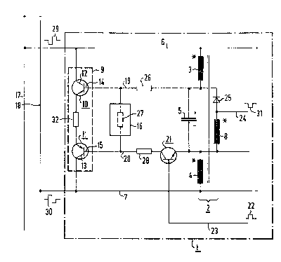
An embodiment of an information separation device 1
according to the present invention shown in FIG. 1, has a
5a
~0~549
transformer 2 that acts as a filter for separating the trans-
mitted direct current power from the a.c. voltage information
being signal. However, according to the invention, only the
information that is received is transmitted via the trans-
former 2. The transformer 2 has at least two windings 3 and 4
on the transformer side which is connected to the direct
current power. A capacitor 5 is serially arranged between
these windings 3 and 4. This capacitor 5 acts as a conductor
for information bearing signals received and represents a
barrier for the direct current power. When the capacitor 5
has a suitable capacity, i.e., is designed as a storage
capacitor, it can in the event of short, external voltage
interruptions, buffer the do voltage on the transmission lines
6 and 7 supplying the direct current power to the information
separation device 1. For receiving direct current power and
the alternating voltage information, the end of the coil 3
that is not coupled to the capacitor 5 is coupled to the
transmission line 6. Likewise, the end of coil 4 not coupled
to the capacitor 5 is coupled to the transmission line 7. The
transformer 2 operates with a winding 8 on the side that
outputs the received information.
A circuit 9, e.g., a push-pull circuit, with two
controllable switches of opposite polarity has its output
electrodes 12 and 13 coupled between the transmission lines 6
and 7. Control electrodes 14 and 15 of the circuit 9 are
coupled to a load-independent voltage source 16 when a
transmission signal is applied to the circuit. In this
manner, a transmitter is provided that, with regard to the
transformer 2, is enabled on the coupling side of the
-6-
20365-3012
200~~~9 ~~~ ~ ~ ~r:~~
information separation device 1.
The information separation device 1 is coupled to a
power source (not shown) via a bus line having bus conductors
17 and 18 in the embodiment of FIG. 1. For the transmit mode,
the switch 21 e.g. a transistor controlled by a transmission
voltage 22 is intercoupled into one of the connection lines 19
and 20. In the embodiment of FIG. 1, the transistor 21 is in
the connection line 20, which extends between the capacitor 5
and the winding 4 on the side of the transformer coupled to
direct current power. A positive transmission signal 22 is
supplied to the transistor 21 via a transmission line 23.
During reception, a receiving line 24 is coupled to
one end of the winding 8 on the transformer side that outputs
the received information. A switch 25, a diode in the FIG. 1
embodiment, acts as a receiver. The receiving line 24 is
connected to the junction between this diode 25 and the
winding 8.
The controllable switches of opposite polarity 10
and 11 are, in the embodiment of FIG. 1, an npn-transistor for
the switch 10 and a pnp-transistor for the switch 11. In the
embodiment of FIG. 2, the switch 10 is an N-channel MOSFET and
the switch 11 a P-channel MOSFET.
The load-independent voltage source 16, as illus-
trated in FIG. 1, is part of a voltage divider comprising at
least three serially-connected resistors 26, 27 and 28 on
whose middle resistor 27 the load-independent voltage is
developed. The voltage divider is coupled to the capacitor 5
via the transistor 21 controlled by the transmission voltage.
The voltage divider with the resistors 26, 27 and 28 can be
-7-
20365-3012
OA~~~9
' ~ ~~~~
switched on and off symmetrically on both sides by including a
switch (not shown) up-stream from the resistor 26. Using both
this switch and switch 21 further promotes a performance
response that is symmetrical and insensitive to interferences.
The information separation device 1 is supplied with
positive do voltage from bus conductor 17 and negative do
voltage from bus conductor 18. The bus conductors each supply
symmetrical alternating voltage signals 29 and 30. The do
voltage is maintained at the ends of the transmission lines 6
and 7 in the information separation device 1. When there is a
negative information bearing signal present on the trans-
mission line 6 and a positive information bearing signal
present on the transmission line 7, the alternating voltage of
the information bearing signal received leads to a flow of
current across the capacitor 5 and a transmitted voltage in
the winding 8. The winding sense is illustrated by an
asterisk so that in FIG. l, in the case of a negative signal
on the winding 3, a negative receiving signal 31 is present on
the winding 8. At the end of the signal the magnetic lagging
of the winding 8 leads to the generation of a relatively
higher positive spike on the winding 8. This higher spike is
sent to the free-wheeling circuit over the diode 25 and the
capacitor 5.
When a positive transmission signal 22 is present on
the transmission line 23, the switch 21 controlled by the
transmission voltage becomes conductive so that the switch 11
also becomes conductive. Due to the coupling across the res-
istor 27, the switch 10 will also be conductively controlled.
In FIG. 1 a limiting resistor 32 is serially coupled between
_g_
20365-3012
~0 A~~~r9
'REV F : .. . ,
the switches of opposite polarity 10 and 11 in order to limit
the current. For reasons of symmetry, it is advantageous to
arrange the limiting resistor 32 between the switch 10 and 11.
Alternatively, the limiting resistor 32 can be included within
the switches of opposite polarity 10 and 11.
In order to operate the switches of opposite
polarity 10 and 11 by the load-independent voltage source 16,
the load-independent voltage source 16 advantageously uses
part of the voltage divider with the resistors 26, 27 and 28.
In place of the middle resistor 27 or in connection with it,
another suitable means of switching can also be used, for
example a Zener-diode. Even when nothing is being trans-
mitted, a fully symmetrical load appears between the trans-
mission lines 6 and 7 when the switches 10 and 11 are closed.
In this manner, no interfering signals can be transmitted on
the bus conductors 17 and 18.
Due to the load-independent voltage source 16, the
information separation device 1 according to the present
invention operates with a load-independent current in the
circuit 9 with the two switches of opposite polarity 10 and
11. This provides a transmit mode that is insensitive to
interferences.
The illustrated embodiment of the information
separation device 1 of the present invention uses a voltage
divider for the load-independent voltage source 16, limits the
voltage during transmit mode and limits the current through
the limiting resistor 32, and simulates the performance char-
acteristics of a typical transformer. When the amplitude of
the transmission voltage and the transmission current is
-9-
20365-3012
~OA~~~9
limited, the transmit mode becomes insensitive to inter-
ferences on the bus, especially to short-circuits on the bus.
On the other hand, during the transmit mode, transmitting
power bypasses the transformer 2 since the transmitting power
is emitted between the transformer and the bus. The trans-
former can thus be designed in a compact and economical
manner, and a bus-sided transmit mode attained.
-10-
20365-3012