Note: Descriptions are shown in the official language in which they were submitted.
20(~4'76
PHA 1180 1 26.10.1989
Differential amplifier using voltage level shifting to
achieve rail to-rail input capability at very low power
supply voltage.
The invention relates to an electronic circuit for
amplifying a circuit input signal differentially provided
between first and second input teL ; nal S as respective
first and second input voltages, the circuit comprising:
main supply means, coupled between respective
sources of a high supply voltage VHH and a low supply
voltage VLL whose difference is a power supply voltage Vps
that defines a power supply range, for providing opposite
first and second operating currents;
first differential means for amplifying the voltage
difference between first and second input points by largely
dividing the first operating current into a pair of
amplified first internal signals, the first and second
points being respectively coupled to the first and second
terminals, the first means being operatively conductive to
so produce the first internal signals when the common-mode
voltage VcM of the circuit input signal is in a portion of
the supply range extending up to VH~;
second differential means for amplifying the
voltage difference between third and fourth input points
by largely dividing the second operating current into a
pair of amplified second internal signals, the third and
fourth points being respectively coupled to the first and
second terminals, the second means being operatively
conductive to so produce the second internal signals when
VcM is in a portion of the supply range extending down to
VLL such that at least one of the differential means is
operatively conductive as VcM traverses substantially the
entire supply range when Vps is greater than or equal to a
specified ~in; level; and
Yl ; ng means for combining the internal signals
to generate at least one circuit output signal;
2~9~'7t;
PHA 1180 2 26.10.1989
Such a circuit is known from US Patent 4,555,673
and relates to a differential amplifier suitable for use in
an operational amplifier ("op amp") made in semiconductor
integrated circuit form and, more specifically, ~o a
differential amplifier that employs complementary
differential portions to attain rail-to-rail input
capability.
An integrated circuit often needs a lower power
supply voltage to avoid heat-dissipation problems.
Low supply voltage will be even more necessary in the
future as integrated circuits become increasingly more
dense. It thus becomes desira~le that a dif~erential
amplifier used as an input stage in an op amp have rail-to-
rail input capability. That is, the output signal of the
amplifier should be representative of the differential
input signal as its common-mode voltage travels the full
range of the power supply voltage. As used here to describe
the relationship between two signals, "representative"
means that their amplitudes have a substantially one-to-one
(typically linear) relationship as long as the amplitudes
are not too great.
Referring to the drawings, Fig.l illustrates a
general arrangement for a prior art differential amplifier
that can achieve rail-to-rail input capability at
moderately low power supply voltage. See U.S. Patent
4,555,673. Also see U.S. Patents 4,463,319 and 4,532,479.
The amplifier in Fig. 1 employs a pair of
complementarty differential input portions 10 and 12 to
amplify a circuit input signal differentially supplied
between input terminals Tl and T2 as input voltages VI1 and
VI2. Differential portion 10 consists of NPN transistors Q1
and Q2 whose bases receive the circuit input signal at
input points Pl and P2 connected to te~ ; n~ ls Tl and T2.
The emitters of transistors Q1 and Q2 are connected
together at a node NA to receive a first operating current
IA. Differential portion 12 is formed with PNP transistors
Q3 and Q4 whose bases receive the circuit input signal at
input points P3 and P4 connected to terminals Tl and T2.
200~
PHA 1180 3 26.10.1989
The emitters of transistors Q3 and Q4 are connected
together at a node NB to receive a second operating
current IB. A main current supply 14 connected between
sources for a high supply voltage VHH and a low supply
voltage VLL provides currents IA and IB in opposite flow
directions.
Portion 10 supplies amplified internal currents IBl
and IB2 from the Ql and Q2 collectors. Portion 12 similarly
provides amplified internal currents ID3 and ID4 from the
Q3 and Q4 collectors. A summing circuit 16 connected
between the VHH and VLL supplies suitably combines currents
IDl - ID4 to generate a pair of complementary output
currents Io and Io.
In looking at amplifier operation, it is convenient
to define several terms. Let "-V" and I~vcM" respectively
represent the differential voltage VIl - VI2 and the
common-mode voltage (VIl + VI2)/2 of the circuit input
signal. Let ''Vps'' represent the power supply voltage VHH -
VLL.
The prior art device in Fig.l can be characterized
by a pair of threshold voltages VTA and VTB that may vary
with Vps. Fig.2 shows a general example of how VTA andVTB
may appear. Fig 3 shows the resulting operational regions
for the amplifier. The horizontal axis in Fig.3 represents
the condition where VcM equals VLL. Line 18 (at 45~)
represents the condition where VcM equals VHH. The region
between the horizontal axis and line 18 thereby encompasses
the rail-to-rail operational range for the amplifier.
Input portion 10 is operatively conductive (turned
on) when VcM is sufficiently high. More specifically:
VcM - VLL 2 VTA- ~1)
Eq. (1) basically corresponds to the portion of the Vps
range between line 20A and line 18 in Fig. 3. The
conductive region for portion 10 does, however, extend
slightly above line 18 to a point where VcM is several
tents of a volt more than VHH. When portion 10 is turned
on, it amplifies the voltage difference between points Pl
and P2 by splitting current IA between currents ID1 and ID2
~oo~
PHA 1180 4 26.10.1989
at values whose difference is representative of ~V.
Input portion 12 is operatively conductive when VcM
is sufficiently low. In particular:
VHH - VCM ~ VTB (2)
Eq. (2) basically corresponds to the portion of the Vps
range between the horizontal axis and line 20B in Fig. 3.
In addition, the conductive range for portion 10 extends
slightly below the horizontal axis to a point where VcM is
several tenths of a volt less than VLL. When portion 12 is
turned on, it amplifies the voltage difference between
points P3 and P4 by splitting current IB between current
Ip3 and Ip4 at values whose difference is representative
of V.
Fig. 3 indicates that portion 10 is turned off i~
the space between the horizontal axis and line 20A -- i.e.,
when VcM - VLL is less than VTA. Likewise, Fig.3 shows
portion 12 as being turned off in the area between line 20B
and 18. This corresponds to the condition in which VHH -
VcM is less than VTB. In actually, each of portions 10 and
12 usually switches between on and off over a spacing on
the order of 100 millivolts. Lines 20A and 20B are thus
idealizations of narrow voltage regions.
When Vps is reduced, the amount of VcM space
available for the non/conductive regions for portions 10
and 12 decreases. The two non-conductive regions start to
overlap when Vps reaches a level VpsO. If Vps drops below
VpsO, VcM passes through a "dead zone" indicated by thick
line 22 in which neither of portions 10 and 12 is
operatively conductive. VpsO is thus the value of the
minimum Vps level at which the differential amplifier in
Fig. 1 can achieve rail-to-rail input capability.
Threshold VTA and VTB have respective ; n; ,
values VMA and VMB. See lines 24 and 26 in Fig. 3. In known
embodiments of the amplifier in Fig. 1, VpsO is
approximately equal to VMA -~ VMB.
The numerical value of VpsO depends on the base-
emitter voltages of transistors Q1 - Q4 and on the internal
construction of current supply 14. Figs. 4a and 4b depict
X01~9~7ti
PHA 1180 5 26.10.1989
two ways, both described in U.S. Patent 4,555,673, for
implementing supply 14. Figs. 5a and 5b graphically show
the specific idealized operational regions for the
amplifier of Fig. 1 as implemented with the main current
supplies shown respectively in Figs. 4a and 4b.
Starting with the embodiment of Fig.4a, supply 14
consists simply of a pair of current sources SL and SH.
Current source SL supplies current IA at a constant value
IL. Current source SH provides current IB at a constant
value IH. For current source SL and SH to be conductive,
the voltage across each of them must be at least equal to a
minimum level VSAT
V~M exceeds the voltage at node NA by lVBE when
portion 10 is turned on. VBE is the magnitude of the
standard voltage across the base-emitter junction of a
bipolar transistor when it is just turned on. The voltage
at node NB similarly exceeds VcM by lVBE when portion 12 is
turned on. In view of this, each of threshold ;n; ~ VMA
and VMB equals VBE ~ VsAT. VpSO thereby equals
2VBE + 2VSAT
At a standard collector-emitter current of several
microamperes, VBE is approximately 0.6 volt. VSAT can be as
low as 0.1 voltO using these values for VB~ and VSAT (in
the present computation and in all the additional ones
below), VpSO is approximately 1.4 volts for the
differential amplifier of Figs. 1 and 4a.
A disadvantage of using the current supply in
Fig. 4a is that the transconductance of the amplifier
changes by a factor of approximately 2 whenever either of
portions 10 and 12 turns on or off. The variation in
transconductance makes it difficult to optimize the
frequency compensation for the amplifier when it is used
in an op amp with negative feedback. The implementation
shown in Fig. 4b overcomes this problem.
When the circuitry of Fig. 4b is used, supply 14 is
formed with current source SH, a PNP steering transistor QP
whose base receives a reference voltage VRp, and a current
mirror 28 that supplies current IA at a value largely equal
;~0~9'~
PHA 1180 6 26.10.1989
to the current IQp through transistor QP. Current steering
through transistor QP enables the sum of IA and IB to
approxima~ely equal IH. As a result, the transconductance
is nearly constant as VcM varies across the entire Vps
range.
The voltage across current mirror 28 between node
NA and the VLL supply must be at least lVSAT for mirror 28
to be conductive. Under optimum conditions, the current
steering causes lines 2OA and 2OB in Fig. 3 to merge into a
single line 20 separated from line 18 by a vertical
displacement equal to VMB as depicted in Fig. 5B.
VMA equals VBE + VsAT again- VMB may be as low as
VBE + VsAT. Consequently, VpsO may again be equal to
1.4 Volts.
As the above discussion indicates, the lowest
tolerable value for Vps in the differential amplifier of
Fig. 1 is approximately 1.4 volts. In practice, Vps may
have to be a few tenths of a volt higher. While this is
still relatively good, it would be quite useful to get down
to 1.0 volt or less. For example, a single-cell battery
having an unloaded rating of 1.5 volts typically drops down
to about 1.0 volt under loaded conditions near the end of
its life. The amplifier of Fig. 1 cannot operate
efficiently from such a battery.
It is the object of the invention to provide a
differential amplifier that can achieve rail-to-rail input
capability at a very low power supply voltage. In bipolar
embodiments/ the power supply voltage can be at or slightly
below 1.0 volts. This makes the invention particularly
attractive for future low-voltage op amp applications.
The invention can be powered from a single-cell 1.5-volt
battery during the entire battery life.
According to the invention a circuit asset forth in
the opening paragraph is characterize in that the circuit
further comprises:
level-shift means for selectively causing the
voltages at the first and second points to be respectively
higher than the first and second input voltages by
~(~0~4'7~i
PHA 1180 7 26.10.1989
respective first and second voltage level shifts and for
selectively causing the voltages at the third and fourth
points to be respectively lower than the first and second
input voltages by respective third and fourth voltage level
shifts.
The level shift means extend the conductive
operational ranges of the differential means so as to
reduce the value of the ; n; level of the power supply
voltage at which the differential amplifier achieves rail-
to-rail input capability.
The circuit may be characterized further in that
the level-shift means comprises:
network means, coupled between the teL ;n~ls and
the points, for providing the level shifts; and
level-shift supply means for providing current to
the network means to control the values of the level
shifts.
The network means may be characterized in that the
network means comprises a first level~shift element coupled
between the first te~ ; n~ 1 and the first point, a second
level-shift element coupled between the second teL ; n~l and
the second point, a third level-shift element coupled
between the first te~ ;nAl and the third point, and a
fourth level-shift element coupled between the second
25 teL ; nal and the fourth point.
The level shift supply means may be characterized
in that the level-shift supply means comprises a first
current source coupled between the first point and the V~H
source, a second current source coupled between the second
point and the VHH source, a third current source coupled
between the third point and the VLL source, a fourth
current source coupled between the fourth point and the V
source, and control means for controlling conduction of the
current sources. The control means preferably operates in
such a way as to gradually turn off the level-shift means
as the power supply voltage rises to a point where level
shifting is not needed.
Embodiments of the invention will now be described,
Z0C~94~76
PHA 1180 8 26.10.1g89
by way of example, with reference to the accompanying
drawings, in which:
Fig. 1 shows a block and circuit diagram of a prior
art differential amplifier,
Figs. 2 and 3 show graphs depictiny operational
features for the amplifier of Fig. 1,
Figs. 4a and 4b show circuit diagrams of prior art
embodiments of the main current supply in Fig. 1,
Fig. 5a and 5b show graphs showing the primary
operational regions for the amplifier of Fig. 1 as
respectively embodied with the current supplies of Figs. 4a
and 4b,
Fig. 6 shows a block diagram of a general
differential amplifier in accordance with the invention,
Fig. 7a and 7b show graphs generally illustrating
the operational regions for the amplifier of Fig. 6,
Fig. 3 show a block diagram of an e~bodiment of the
level-shift current supply in Fig. 6,
Fig. 9a, 9b, and 10 show graphs generally showing
operational aparameters for the amplifier of Fig. 6 as
embodied with the circuitry of Fig. 8,
Fig. 11 shows a block and circuit diagram of a
general embodiment of the amplifier of Fig.6,
Fig. 12 shows a block diagram of an embodiment of
the level-shift current control in Fig. 11,
Figs. 13a, 13b, and 13c show graphs illustrating
how level-shift voltage preferably varies as a function of
input common-mode voltage for the amplifier of Fig. 11,
Figs. 14a and 14b show graphs showing the
operational regions for the amplifier of Fig. 11 as
respectively embodied with the currents supplies of
Figs. 4a and 4b,
Fig. 15 shows a circuit diagram of a preferred
bipolar embodiment of the amplifier of Fig. 11,
Fig. 16 shows a circuit diagram of a preferred
embodiment of the reference voltage circuitry in Fig. 15,
Fig. 17 shows a graph illustrating the operational
regions for the amplifier of Fig~ 15 as embodied with the
2~1~9~
PHA 1180 9 26.10.1989
complete reference voltage circuitry in Fig. 16,
Figs. 18a and 18b show graphs showing an
alternative variation for level-shift current as a function
of input common-mode voltage for the amplifier of Fig.11,
Fig. 19 shows a graph illustrating the operational
regions for the amplifier of Fig.ll as embodied with the
current supply of Fig.4a for the level-shift variation
indicated in Figs. 18a and 18b and
Fig. 20 shows a block and circuit diagram of
another general embodiment of Fig. 6.
Like reference symbols are employed in the drawings
and in the description of the preferred embodiments to
represent the same or very similar item or items.
Referring to Fig.6, it illustrates a general
arrangement for a differential amplifier that amplifies a
circuit input signal differentially supplied between input
tel in~ls Tl and T2 as input voltages VIl and VI2.
This differential amplifier uses a level-shifting
technique in accordance with the invention to attain rail-
to-rail capability for the common-mode voltage VcM of the
circuit input signal at Yery low power supply voltage.
The amplifier is particularly suitable for use as an input
stage of a low-voltage op amp fabricated in semiconductor
integrated circuit form.
The device in Fig. 6 centers around complementary
differential input portions 30 and 32. Differential
portion 30 consists of like-configured three-electrode
input amplifiers Al and A2. Differential portion 32 is
formed with like-configured three-electrode input
amplifiers A3 and A4 which are complementary to amplifiers
Al and A2. The term "complementary" means opposite
polarity.
Amplifiers Al - A4 are referred to here as the "A"
amplifiers. Each "A" amplifier has a first flow electrode
(lE), a second flow electrode ~2E), and a control electrode
(CE~ for controlling current flow between the flow
electrodes (lE and 2E). Charge carriers, either electrons
or holes, that move between the flow electrodes of each "A"
Z0~ '7~:i
PHA 1180 10 26.10.1989
amplifier originate at its first flow electrode and
terminate at its second flow electrode. The current (if
any) flowing in the control electrode is much smaller than
that otherwise moving between the flow electrodes.
Each "A" amplifier preferably consists of a single
transistor. In the case of a bipolar transistor, its
emitter, collector, and base are respectively the first,
second, and control electrodes. These elements are
respectively the source, drain, and gate for a field-
effect transistor of either the insulated-gate or junction
type.
Although generally undesirable, each "A" amplifier
could consist of more than one trans~stor. One example is a
bipolar Darlington circuit in which the emitter of an input
transistor is connected to the base of a trailing
transistor. In this case, the control electrode of the "A"
amplifier is (connected to) the base of the input
transistor, while the ~irst and second control electrodes
are (connected to) the emitter and collector of the
trailing transistor.
As used in describing amplifiers Al and A2 or A3
and A4, "like-configured" means that the two amplifiers in
question have corresponding elements interconnected in the
same way and that each sst of corresponding elements is of
the same semiconductor polarity. For example, amplifiers Al
and A2 are like-configured if both are NPN transistors but
not if one is an NPN transistor while the other is a PNP
transistor. Likewise, Darlington circuits are like-
configured as long as the input transistors are of the same
polarity and the trailing transistors are of the same
polarity (even if different from that of the input
transistors).
Turning back to Fig.6, the first electrode of
amplifiers Al and A2 are connected together to receive
operating current IA at node NA. Similarly, amplifiers A3
and A4 have their first electrodes connected together to
receive operating current IB at node NB. A main current
supply 34 connected between the VHH and VLL supplies
213~4'7~j
PHA 11~0 11 26.10.1989
provides oppositely directed currents IA and IB. Current
supply 34 may be implemented using either of the circuits
shown in Figs. 4a and 4b. Other embodiments described in
U.S. Patent 4,555,673 may also be used.
Differential portions 30 and 32 function in a
complementary manner. When VcM is sufficiently high,
portion 30 amplifies the voltage difference between input
points Pl and P2 connected to the A1 and A2 control
electrodes by dividing current IA into amplified internal
currents ID1 and ID2 supplied from the Al and A2 second
electrodes. The difference between the currents IDl and ID2
is representative of the voltage difference between points
Pl and P2. When VcM is sufficiently low, portion 32
amplifies the voltage difference between input points P3
and P4 connected to the A3 and A4 control electrodes by
dividing current IB into amplified internal currents ID3
and ID4 supplied from the A3 and A4 second electrode. The
difference between currents I~3 and ID4 is representative
of the voltage difference between points P3 and P4.
A summing circuit 36 connected between the VHH and
VLL supplies suitably combines curruents ID1 - ID4 to
produce complementary circuit output currents Io and Io.
Summing circuit 36 may be implemented in any of the ways
shown in U.S. Patents 4,555,673 and 4,532,479. If desired,
circuit 36 may provide only a single circuit ou~yut
current.
A level-shift circuit consisting of a network of
level-shift elements 38, 40, 42, and 44 and a level-shift
supply circuit 46 selectively enables voltages Vpl and Vp2
at points P1 and P2 to exceed voltages VI1 and VI2 by
controllable level shifts VLsl and VLS2~ The level-shift
circuit likewise selectively enables voltages Vp3 and Vp4
at points P3 and P4 to be less than voltages VIl and VI2 by
controllable level shifts VLS3 and VLs4. Level shift
elements 38 - 44, which are connected between teL ;n~1s Tl
and T2 and points Pl - P4 in the manner shown in Fig. 6,
directly provide level~shift voltages VLsl - VLs4.
Level-shift current supply 46, which is connected
2(~4'7~;
PHA 118Q 1~ 26.10.1989
between the VHH and VLL supplies, controls the operation of
level shifts 38 - 44. Current supply 46 accomplishes the
control by providing supply currents ISl~ IS2~ Is3 and Is4
along lines connected to points Pl - P4. Although not
indicated in Fig. 6, supply 46 is typically connected to
other points in the amplifier circuit. For example, supply
46 may provide current at te. in~l S Tl and T2 in some
embodiments of the invention.
As indicated in Fig. 6, level-shift currents ILSl,
ILSl~ ILS3~ and ILS4 actually flow through elements 38 -
44- Currents ILSl ~ ILS4 respectively differ from currents
ISl - Is4 by the currents (if any) flowing through the
respective control electrodes of amplifiers A1 - A4. The
control-electrode current normally can be neglected. As a
result, each level-shift current ILSi is substantially
equal to corresponding supply current ISi (where i is 1, 2,
3, or 4).
To have a good common-mode rejection ratio, VLSl
and VLS2 are preferably equal. Consequently, ILSl and ILS2
are preferably equal. Likewise, VLs3 and VLs4 are
preferably equal so that ILS3 and ILS4 are also preferably
equal.
It is desirable to avoid loading the circuitry that
supplies circuit inputs VIl and VI2. Except for the
situation in which other internal current of significant
magnitude is supplied at terminals Tl and T2, this
objective can usually be reached by setting ILS3 equal to
ILSl. Likewise, ILS4 is usually chosen to equal ILS2.
The result is that currents ILSl and ILS4 are typically all
equal. Nonetheless, voltages VLs3 and VLs4 may still
respectively differ from voltages VLs1 and VLs2.
Current supply 46 utilizes currents I2Sl - Is4 to
control the values of voltages VLSl ~ VLS4 in a way that
reduces the minimum rail-to-rail VcM level for the power
supply voltage to a value lower than that which would be
ne~ded if (a) Vpl and Vp3 always equalled VIl and (b) Vp2
and Vp4 always equalled VI2O An understanding of how the
level-shift control is accomplished can be facilitated by
200~
PHA 1180 13 26.10.1989
first considering what would happen if components 38 - 46
were absent. In that case, the operation would proceed
basically in the manner described above for the
differential amplifier of Fig. 1. When power supply voltage
VPS drops below prior art value VpsO, VcM would pass
through (at least part of) the dead zone in which neither
of portions 30 and 32 is operatively conductive.
With the level-shift circuit present, the operation
can still be described in terms of thresholds VTA and VTB
~hown in Fig.2. However, VcM in Eq. (1) must be replaced
with the common-mode voltage VCMA at points Pl and P2.
Differential portion 30 is turned on when:
VCMA ~ VLL 2 VTA
In view of Eq. (3), VLSl and VLS2 must be related to VTA as
follows in order to make portion 30 operatively conductive
if VcM is not high enough in itself to turn portion 30 on:
VLSl/ VLS2 2 VTA ~ VCM - VLL (4)
Because supply 46 operates from the VHH supply, Eq. (4) is
at least subject to the limitation that:
VLSl~ VLS2 < VHH ~ VCM ( )
VcM in Eq. (2) must similarly be replaced with the
common-mode voltage VcMB at points P3 and P4. Portion 32 is
turned on when:
VHH - VCMB 2 VTB (6)
Accordingly, VLs3 and VLs4 must satisfy the following
relationship with VTB so as to make portion 32 operatively
conductive if VcM itself is not low enough to turn portion
32 on:
VLS3~ VLS4 2 VTg = VCM - VHH (7)
Since supply 46 also operates from the VLL supply, Eq. (7)
is at least subject to the restriction that:
VLS3~ VLS4 < VCM ~ VLL (8)
A level shift is usually not needed when Vps is
greater than VpsO (since VcM will be sufficient in itself
to cause one or both of portions 30 and 32 to turn on).
When Vps is less than VpSO so that a level shift is needed,
thresholds VTA and VTB are preferably at their respective
minimum values VMA and VMB. As a result, V~A and VMB can be
200~4'7~i ~
PHA 1180 14 26.10.1989
respectively substituted for VTA and VTB in Eq. (4) and
(7).
Let VSATH be the minimum voltage spacing that
supply 46 allows between VHH and the highest of Vpl and
Vp2. Likewise, let VSATL be the minimum voltage spacing
that supply 46 permits between VLL and the lowest of Vp3
and Vp4. When Vc~ is not adequate by itself to cause at
least one of portions 30 and 32 to become conductive,
supply 46 thereby normally provides currents ISl - Is4 at
values that enable level shifts VLSl - VLs4 to satisfy the
following relationships:
VHH ~ VCM - VSATH 2 VLsl, VLS2 2 VMA ~ ~CM + VLL (9)
VCM ~ VLL ~ VSATL ~ VLS3~ VLS4 2 VMB + VCM VHH (10)
For the situation in which V~A and VTB vary in the
manner indicated in Fig. 2, Figs. 7a and 7b show the
operational regions that result from using the level-shift
circuit. Fig. 7b is a 3X magnification of a lower portion
of Fig. 7a encompassing the VMA-to-Vps0 part of the Vps
range. Lines 1~, 24, and 26 are the VHH, VMA, and VMB lines
as in Fig. 3. Lines 20A, 20B, and 22 of Fig. 7a have the
same meaning for the invention that lines 20A, 20B, and 22
have in Fig. 3 for the prior art circuit of Fig.1.
The point where the non-conductive region for
portion 30 starts to overlap with the non-conductive region
for portion 32 occurs when Vps is at a value VpsF as
indicated in Fig.7a. This is the lowest value of the power
supply voltage at which the differential amplifier of
Fig. 6 can achieve rail-to-rail input capability. Due to
the level shift, VpsF is less than VpsO. For the usual case
in which Vpso equals VMA + VM~, VpsF is thus less than
VMA + VMB-
The low~r limit for VpsF is slightly greater than
the larger of VMA and VMB in the normal situation. More
specifically, VpSF usually equals (a) VMA + VSATH or ~b)
VMB + VSATL~ whichever is larger.
Turning briefly to Fig. 7b, the three different
zones of the triangular operational region formed by lines
22, 24 and 26 are labeled with reference numbers 48, 50,
Z0094'7~:i
PHA 1180 15 26.10.1g89
and 52. If VcM is in zone 48, the level-shift circuit
preferably adjusts VLSl and VLS2 according to Eg. (9) so as
to turn portion 30 on. If VcM is in zone 50, the level-
shift circuit preferably adjusts VLs3 and VLs4 according to
Eq. (10) in order to turn porton 32 on. Finally, the level-
shift circuit adjusts VLsl - VLs4 according to Eqs. (9~ and
(10) so as to turn on both of portions 30 and 32 when VcM
is in zone 52.
Fig. 8 illustrates in general functional embodiment
for current supply 46 in Fig. 6. In this embodiment, a
common-mode generator 54 responsive to circuit inputs VIl
and VI2 produces operating voltages VyA and VyB that bear
specific relationships to Vc~. For example, each of
voltages VyA and VyB may differ from VcM by an amount that
is largely constant at a given temperature. In response to
signals VyA and VyB~ a level-shift current control circuit
56 generates a pair of control voltages VcL and VcH that
control the operation of a set of level-shift current
sources 58 suitably connected between the VLL and VHH
supplies. Sources 58 provide supply currents ISl - Is4.
Turning back to current control 56, it consists of
voltage reference sources 60 and 62, differential
amplifiers 64 and 66, and a linear AND/NAND generator 68.
Reference sources 60 and 62 provide reference voltages VRA
and VRB at values respectively "referenced" to low supply
voltage VLL and high supply voltage VHH. In particular,
VRA typically exceeds VLL by an amount VKA that is largely
constant at a given temperature. VRB is likewise lower than
VHH by an amount VKB ~hat is largely constant at a given
temperature.
Amplifier 64 amplifies the difference between
voltages Vy~ and VRA to produce an amplified voltage VzA
that gradually changes from high level VzD to low level Vzc
as VyA passes VRA. Amplifier 66 amplifies the difference
between voltage VyB and VRB to produce an amplified voltage
VZB that gradually changes from Vzc to VzD as VyB passes
VRB. Figs. ga and 9b respectively show how voltages V~A and
VZB basically vary. Transition zones 70 and 72 in Figs. ga
20(~9~76
PHA 1180 16 26.10.1989
and 9b are typically 100 millivolts in width.
Generator 68 supplies (a) control voltage V~L as
the linear AND of voltages VzA and VzB and (b) control
voltage VcH as the linear NAND of voltages VzA and VzB.
Referring to Fig.10, the top curve depicts how voltage VcL
varies between low level VcLc and high level VCLD as a
functi~n of VCM-
Transition zones 70 and 72 for VzA and VzB are
reflected in VcL as respective transition zones 74 and 76.
The centres of zones 74 and 76 are respectively
"referenced" to VLL and VHH. That is, the center of zone 74
is separated from VLL by a voltage spacing VCLL that is
largely constant at a given temperature. The center of zone
76 is similarly separated from VHH by a voltage spacing
that is largely constant at a given temperature. As a
consequence, the separation between zones 74 and 76 varies
inversely with vps.
Fig.10 indicates that the VcL curve has a flat
portion 78 situated between zones 74 and 76. It is usually
preferably that zones 74 and 76 meet so that portion 78
compresses to a point. If zones 74 and 76 do so meet, an
increase in Vps causes zones 74 and 76 to merge into each
other. High level VCLD decreases in value.
Typical level shift VLsi vary when control voltage VcL
(or VcH) has the indicated variation. Zones 74 and 76 are
reflected directly in the I5i and VLsi curves. If a
sufficient increase in Vps causes zones 74 and 76 to merge,
high levels ISM and VLSM for the ISi and VLSi curves
usually decrease. In this way, the level-shift circuit
gradually shuts off as Vps rises.
Moving to Fig. 11, it shows an embodiment of ~ig. 6
in which amplifiers Al - A4 are formed with bipolar
transistors Ql - Q4 arranged the same as in Fig. 1. Level
shifts 38 - 44 ar~ embodied with resistors R1, R2, R3, and
R4 in Fig.ll. Common-mode generator 54 of Fig.8 is
implemented with components 30, 32, 34, and Rl - R4 in
Fig.11. These components in combination with current supply
56 form a level-shift feedback control loop. Finally,
z~
PH~ 1180 17 26.10.1989
current sources 58 of Fig. 8 are implemented with variable
current sources Sl, S2, S3, and S4 in Fig.ll. Signal VcH
controls current sources S1 and S2, while signal VcL
controls current sources S3 and S4.
In Fig. 11, VMA equals VBE + VsAT when main supply
34 is implemented with the circuitry of Fig. 4a or 4b.
For the optimum case in which VRp equals VHH - VMB in
Fig. 4b, the same applies to VMB. The i n; voltage
across each of current sources Sl - S4 when they are fully
conductive is lVSAT. Since each spacing VSATL or VSATH
thereby equals lVSAT, Vpss equals VBE ~ 2VSAT- Using the
above values of 0.6 volt for VBE and 0.1 volt for VSAT~
VPSF is approximately 0,8 volt.
Fig. 12 depicts a preferred way for implementing
current control 56 in Fig.ll. The circuitry in Fig. 12
differs from current control 56 in Fig. 8 in that the
circuit of Figh. 12 employs a differential amplifier 78 to
perform the functions of components 66 and 68 in Fig. 8.
Amplifier 78 amplifies the difference between voltages VyB
and VRB just as amplifier 66 does in Fig. 8. However,
amplifier 78 has a gain control terminal that receives
voltage VzA from amplifier 64. This allows amplifier 78 to
produce control voltages VCL and VcH in much the same way
as shown in Fig. 10.
Figs. 13a - 13c indicate the manner in which level-
shift voltage VLSi preferably varies as a function of VcM
for the differential amplifier of Fig. 11 when implemented
with current control 56 of Fig. 8 or 12. For the case
illustrated in Figs. 13a - 13c, resistors R1 - R4 all have
the same resistance. Fig. 13a depicts the basic situation
at standard temperature and l.0-volt Vps. Fig. 13b
illustrates how the level-shift circuit gradually "turns
off" as Vps increases. No level shifting is needed when Vps
is at or above 1.4 volts. As indicated in Fig. 13c, the
level-shift circuit also automatically increases VLSi with
decreasing temperature, and vice versa, to provide
temperature compensation.
Figs. 14a and 14b graphically show the idealized
xo~
PHA 1180 18 26.10.1989
operational regions that arise for the differential
amplifier of Fig.ll when main current supply 34 is
respectively embodied with the circuitry of Figs. 4a and
4b. In Fig. 14a, the merged portion of lines 20A and 20B
lying between VpSO and VpsF is equally separated from YLL
and VHH. The same applies to the portion of line 20 located
between VpFo and VpsF in Fig. 14b.
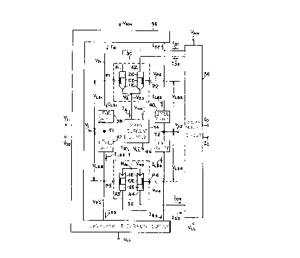
A preferred bipolar embo~; ~nt for the present
differential amplifier is shown in Fig. 15. Subject to the
following comments, the elements used in Fig. 15 to
implement the components of the amplifier of Fig. 11 can be
determined by inspection. Main supply 34 is implemented
with the circuit of Fig. 4b. Consequently, the
transconductance of the amplifier in Fig. 15 is largely
constant. A voltage reference source 80 supplies reference
voltage VRp at a value lower than voltage VHH by an amount
VKp that is largely constant at a given temperature.
For supply 34 to operate optimally, VKp equals VBE + VsAT.
That is, VRp equals VHH ~ VBE ~ VSAT-
Current control 56 in Fig. 15 uses the arrangement
shown in Fig.12. Based on what has been said above about
Fig. 12, a detailed underst~n~;ng of the various circuit
elements in control 56 should be evident to a skilled
artisan. Resistors Rl - R4 introduce an extra frequency
pole. Capacitors Cl, C2, C3, and C4 provide frequency
compensation by introducing a frequency zero at
approximately the same location as the extra pole.
Fig. 16 illustrates two ways for implementing
voltage reference sources 60, 62, and 80. Using only the
circuit elements shown in solid line, VRB and VRp are
separated from VHH by relatively constant amounts at a
given temperature. Howev~r, it is usually desirable to
employ portion 30 over more of the Vps range than portion
32 because NPN transistors require less base current than
PNP transistors. This objective can be reached by using the
entire circuitry (both solid line and dashed line~ shown
in Fig. 16. The full circuitry in Fig. 16 also avoid Zener
problems that NPN components 30 and 78 might otherwise
Z0(~94~6
PHA 1180 19 26.10.1989
encounter. In this case, Fig. 17 illustrates the resulting
idealized operational regions. The level-shift circuit
shuts off when Vps goes above 1.6 volts.
As indicated above, the level-shift circuit
S normally shuts off when Vps rises. Nonetheless, there may
be some applications in which the level-shift circuit
should remain fully on as Vps is increased. Figs. l~a and
18b indicate how level shift VLSi would vary with VcM in
such an application for the case in which main supply 34 is
implemented with the circuit of Fig. 4a. The basic
variation at a l.0-volt Vps is shown in Fig. 18a. Fig. 18b
illustrates what happens as Vps is raised. Fig. 19 shows
the resulting idealized operational regions.
In the embodiments of the invention variously
illustrated in Figs. 8 - 19, supply currents ISl - Is4 are
all approximately equal. Consequently, portion 30 receives
a level shift when portion 32 receives a level shift, and
vice versa. The level shifts received by portions 30 and 32
are normally close to the same value.
Fig. 20 depicts an embodiment of Fig. 6 in which
the level shifts supplied to portions 30 and 32 are largely
independent of each other. This is achieved by usin~ four
additional variable current sources S5, S6, S7, and S8
arranged as indicated in Fig. 20. Sources Sl, S2, S7, and
S8 fix the level shift for portion 30O Sources S3 - S6
similarly fix the level shift for portion 32.
In addition to control voltages VcL and VcH,
current control 56 in Fig. 20 supplies control voltages
VcL and VcH'. Signals VcH and VcL' are generated at
complementary values to control the level shift for portion
30. Signals VcL and VcH. are likewise supplied at
complementary values to control the level shift for portion
32. However, signals VcL and VcH' do not necessarily track
signals VcH and VCL -
While the invention has been described with
reference to particular embodiments, this is solely for the
purpose of illustration and is not to be construed as
limiting the scope of the invention claimed below. For
Z0~ 76
PHA 1180 20 26.10~1989
example, the level shifts might be implemented with
Schottky diodes to improve the noise behavior. Thus,
various modifications and applications may be made by those
skilled in the art without departing from the true scope of
S the invention as defined in the appended claims.