Note: Descriptions are shown in the official language in which they were submitted.
Description
Capacitive Accelerometer With Separable
Damping and Sensitivity
Technical Field
This invention relates to solid state
accelerometers micro-machined from silicon.
Background Art
In the field of accelerometers, it is known to
form a small compact accelerometer by etching the
relevant parts out of silicon. U.S. Patent
4,574,327 illustrates one version of such,a
transducer in which a proof mass having a textured
surface containing many grooves and apertures
extending through the proof mass has its surface
tailored in order to achieve the desired frequency
response by using the squeeze-film damping
phenomenon. In that apparatus, response is hindered
by the fact that the surface of the proof mass is
corrugated and is not unifor~ so that the
capacitance is much less than it would be if the
, surface were smooth. Further, the removal of a
substantial portion of mass limits the amount of
mass available and thereby decreases the ensitivity
of the accelerometer.
~ Other forms of micro-accelerometers employ
cantilever proof masses that introduce an asymmetry
~ R-3138hsgc
: : - 1 -
:: : ~
~ .
'':
, ;: . .~ ~,;
: ;
~: ..
2~ 9
that can give an undesirable cross-axis sen~itivity.
The preceding '327 patent avoids that asymmetric
effect by showing a flexible hinge all around the
proof mass so that the respon~e i8 directed
preferentially to an axis perpendicular to the
plane of the proof mass.
The problems evidenced by such prior art
devices are the difficulty of tailoring the
parameters of the device to accommodate different
ranges of acceleration to be measured and the
different ranges of freguency response of the
device. In a typical design, the mechanical,
damping and electrical parameter~ are interrelated
so that changing one parameter will have an adverse
affect on others.
Disclosure of Invention
The invention relates to an improved
capacitive accelerometer in which a three-plate
capacitor is formed with the proof mass being the
central plate, and in which the proo~ mass i8
suspended from a silicon frame by means of a novel
arrangement of flexures that have highly improved
symmetry resulting in decreased cross-axis coupling.
Other features and advantages will be apparent
~5 from the specification and claims and from the
accompanying drawings which illustrate an embodiment
of the invention.
Brief Description of Drawings
Fig. 1 illustrates in cros~ section an
embodiment of the invention.
Fig. 2 illustrates in perspective a proof mass
constructed according to the invention.
- 2 -
. ~
2~ 39
Fig. 3 illustrates a plan view of an alternate
version of flexures usable together with the
invention.
Fig. 4 illustrates different shapes of proof
mass usable in the invention.
Best Mode for Carrying Out the Invention
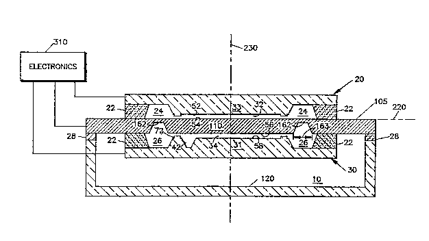
Referring now to Fig. 1, there is shown in
cross section an embodiment of the invention adapted
to register acceleration coaxial with an axis 230
extending upwardly through the drawing. For
clarity, the vertical dimensions are greatly
exaggerated. Electrically, the apparatus is a
three-plate capacitor in which top and bottom plates
20 and 30 respectively are formed of rigid silicon
members that are bonded to an intermediate cilicon
frame 105 that contains a proof mass 110. Bonding,
by means of standard anodic or thermal methods, i~
between frame 105 and glas~ borders 22 formed on the
top and bottom plates 20 and 30 using standard glass
deposition and etching techniques.
Differences between prior art three-plate
capacitor arrangements and that of the present
invention may be illustrated conveniently with
respect to Fig. 2, showing frame 105 and proof mass
110 in simplified perspective. The same axis 230 is
the Z axis in this drawing with corresponding X axis
210 and Y axis 220 which lie an the midplans of the
proof mass and pass through its centroid. Proof
mass 110 is surrounded by a gap 163 formed by
anisotropic etching, illustratively EDP etching. An
important distinction between prior art arrangements
and the present invention is that of the layout of
the flexures, or hinges, which couple proof mass 110
to frame 105. Looking along Y axis 220, it can be
seen that there is a relatively large flexure 162 in
.. ., ~. . . :
.
~ . . .
-' -
2~ 89
the top plane at both the top and bottom of the
drawing. On the bottom surface of proof mass 110,
there is a pair of smaller flexures 164 disposed
symmetrically about Y axis 220, each having half the
width of flexure 162, so that the total stiffness of
the flexures on the top and bottom surface is the
same. Also, on the lower portion of gap 163 on the
opposite side of the proof mass, there i8 a
s~mmetric arrangement of corresponding flexures 162
and 164. Thus, not only is th~ top and bottom of
the arrangement symmetric about axis 220, but also
it is symmetric about X axis 210 since there i8 a
balance on the top and bottom of the drawing.
on the left and right of the drawing, there is
a corresponding symmetric arrangement of flexures
1~4 and 162 that differs from the top and bottom
sides in that the smaller flexures 164 are on the
top surface and the larger one, 162, is on the
bottom surface. The importance of this arrangemont
can be seen by looking at axes 240 and 250,
respectively, which extend along the diagonals of
the square proof mass 110 midplane. Looking at axis
240, for example, there is a flexure 164 on the
bottom surface of proof mass 110 on the left and a
corresponding flexure 164 on the top surface on the
~ight. This would induce a sliqht torgue about axis
240 but that is balanced by corresponding flexures
162 on the bottom right and top left, respectively.
Similarly, about axis 250, thera 1B a corresponding
top/bottom matching of flexures, both flexures being
spaced equally from the corner. For purposes of
this application, the arrangement shown in Fig. 2
will be referred to as being symmetric about the
diagonal plane defined by axes 230 and 240, even
though corresponding flexures are in opposite top or
bottom surfaces of the proof mass.
,
. : : .
.
z~
The flexure layout i5 not, of course, confined
to a three-flexure per side arrangement and many
other arrangements relative to widths, number~ and
placement of the flexures will be evident to those
skilled in the art. Flexures may be placed on the
top and bottom surface~, as shown, or in the
midplane of the proof mass. The principle being
followed in this embodiment is that of high symmetry
about the transverse axes 210 and 220 togeth~r with
sy D etry about the diagonal axes 240 and 250.
Alternative forms of proof mass 110 are
illustrated in Fig. 4A, 4B and 4C. Etching of
square corners in silicon is known to those skilled
in the art to be possible by various technique~
disclosed in the literature, such as "Corner
Undercutting in Anisotropically Etched Contours", by
M.M. Abou-Zaid, in Journal of the Electrochemical
Society, Solid State Science and Technology, Sept.
1984, page 2138. Some expense can be saved by an
arrangement such a~ that in Fig. 4A, in which the
corners are permitted to be "faceted" or non-square.
Fig. 4B has inside corners, which are square, a~
well as outside corners and haæ a longer "lever arm"
for the hinges than for the capacitor which would be
in the central portion. This may be useful for
closed-loop applicationq. It still preserve~ the
symmetry of the embodiment of Fig. 2 about the X and
Y axes and also about the diagonal axes. Fig. 4C
6hows a 12 sided layout that ~ollows the contour~
that naturally result from differential etch~ng.
The proof mass is approximately circular, whi~h aids
in preserving the symmetry of the proof mass about
the acceleration axis. The 4C embodiment would
preferably have springs on four sides, for easa in
fabricating consistent hinges of uniform length in
the gap between the proof mass and the frame.
-- 5 --
, ~
-,, ' ' ,
,
20(~ 39
In the illustrative embodiment, <lOo~ oriented
silicon was the starting material, with the
geometry laid out so that the edges are along the
<110> directions. Anisotropic etching does not
proceed at the same rate in the different crystal
planes.
According to the present invention, the
flexures 162 and 164 are fabricated by masking and
boron doping both top and bottom ~urface~ of a
silicon wafer illustratively 10 mil~ in thickness
such that the limit Or 6xl019 boron atoms per cubic
centimeter is reached at the depth corresponding to
the desired flexure thickness, illustratively 2
microns. With this arrangement, the boron layers, in
the top and bottom surfaces, serve a~ etch stops for
a standard anisotropic etchant, illustratively
ethylenediamine pyrocatohol (EDP), so that when gap
163 is etched, the gap is opened until the boron
layer is reached which serv~s as an etch stop in
those areas where it exists and the etchant opens
the apertures around the gap 163. Pre$erably, the
wafer is etched from both top and bottom at the 3ame
time by immersing in a fluid bath.
Referring back to Fig. 1, it can be ~een that
the cross section is taken through the Y/Z plane
showing two of flexures 162 at the top of proof mass
110. Apertures 24 in the top plate 20 and 26 in
bottom plate 30 have been opened by any convenient
etching method to sharply define the area of the
variable capacitors formed by plates 20 and 30 and
the proof mass 1}0 and also to reduce para~itic
capacitance. When the proof mass is displaced
upward or downward, ga~ will be forced out of the
inter-plate chambers 32 or 34 downward respectively
into these apertures and into other apertures
described below.
.. . . .
;
4~9
It has been found that sub~tantial factor~ in
the temperature and temporal stability of capacitor
transducers are the temperature coefficient and the
aging characteristics of the glass dielectric 22
which bonds together the several plates of the
capacitor. The smaller the bond area and the
greater the thickness of the glass dielectric 22
between plates 20 and 30 and the frame 105, the less
effect the temperature and aging will have on the
capacitance measurement being made. Preferably, the
thickness of bonding glass 22 i8 relatively large
compared with the capacitor gap and the horizontal
dimension of the bonding glass 22 is relatively
small compared with the width of mesa 31. In an
illustrative example, the width of mesas 31 and 33
was about 0.150 inch and the width of the glas~ 22
was about 0.010 inch. Illustratively, the entire
arrangement will be enclosed in a hermetically
sealed enclosure having a pressure chosen for
convenient damping and havinq a gas volume
communicating with apertures 24 and 26 far in excess
of the volume of capacitance chambers 32 and 34 plus
the apertures 24 and 26.
In operation, as the unit i8 accelerated
upwards along axis 230, the proof mass 110 will drop
toward the bottom in the diagram reducing the gap
between surfaces 56 and 58 and thus, the gas volume
in lower chamber 34. Insulating travel stops 72 are
shown as being located at various locations on mesas
31 and 33 in order to prevent the proof mass from
coming in contact with either mesa. These stop~ are
illustratively glass coated in order to prevent
electrical short circu$ts when the proof ma~s
toucheq them and have illustrative dimension~ o~
0.005 inch in width and 0.4 micron in height, with a
glass layer of 0.5 micron in thickness for
.
- 7 -
2(~ 9
insulation. The distanca between capacitor plates
may be controlled conveniently by the thickness of
layer 22, so that the nominal capacitance, and thus
the sensitivity of the sensor, may be altered
without affecting the proof mass.
The squeeze film damping phenomenon is used to
control the frequency response of the proof mass. A
sample channel or passageway is shown that serves to
provide a reservoir to hold displaced ga~ that is
squeezed out from the volume between the plates,
denoted by the numeral 42. This channel will b~
part of a network covering surfaces 58 and 52. As
chamber 34 contracts, gas is forced into or out of
these reservoirs. The total volume of the gas
reservoirs should be considerably greater than the
change in volume of gas chamber 34 so that there
will be only a small increas~ in pressure in the
reservoirs. Preferably, the ratio is about 10 to 1
or greater and the channels have a width of 0.005"
and a depth of 12 microns. Channels 42 are formed
by any of several standard silicon processing
techniques, such as ion milling or reactive ion
etching. Since the passageways are relatively
shallow, little additional surface i8 removed beyond
that associated with their width in spite of the
non-vertical walls that result from a wet etch
process, as illustrated in the figure. In contrast,
if th~ passageways are formed in the proof mass, its
much greater thickness ~typically .01") would
`require deep trenches in order to form the through
holes, thereby removing appreciable mass and surface
area. Thus, the surface area effectively available
for the capacitor is much reduced, and for a given
capacitance the area of the capacitor itsel~ must be
larger. With this arrangement of relatively narrow
shallow trenches in mesas 31 and 33, the affected
-- 8 --
, ,
.
2~
area available for the capacitance measurement is
maximized and, since the proof mass is not pierced
and trenched, maximum inertial mass is retained.
These channels 42 com~unicate with reservoir 26 by
extending perpendicular to the plane of the paper
and/or in the plane of the paper.
The overall arrangement of upper plate 20,
lower plate 30 and frame 105 is supported by a
three-dimensional silicon isolation support frame
120 having a generally U-shaped cross section. It
is connected to frame 105 by joints 28 connected to
support frame contact areas where joints 28 connect
the extension o~ frame 105 and the support members
extending from the base region in the bottom of Fig.
1. These may be insulating or conducting, as
desired. An advantage of this method is that the
thermal effects of heat conduction or los3 to the
outside world are entirely symmetrical relativa to
the upper and lower plates. Experience has shown
that if the device is mounted on lower plate 30, for
example, upper plate 20 will typically be at a
different temperature, with consequent thermal
stresses and distortion introduced by the
temperature differential. Moreover, use of a
di~similar material to mount the accelerometer, such
as an epoxy, results in unacceptably large
asymmetries. Typical temperature performance
achieved with the above described symmetric mount
arrangement results in device sensitivities below 2
ppm/ C. Additionaly, the perferred configuration
is mounting on all four sides of frame 105.
For a given surface area, the capacitance of
the upper and lower capacitors is set by the gap
between the proof mass and the surfaces of the top
and bottom plates. This gap, illustratively 2
microns, is determined both by the thickness of
_ 9 _
. : ~ , .. . .: -
- , .; -. . :: . , : . :
~: . : . , .- , . ;
.~
- .~:, ' . '
- , , ~. . . . :
. ~-. . . ':; :
2~
glass layers 22 which are deposited across the
surface of the wafers and etched away except in
predetermined areas and by the heights of mesas 31
and 33. Consequently, the gap can be controlled
simply by changing the thickness of glass layer 22,
in contrast to other art wherein the gap is set by
removing material from the face of the proof mass.
It is a further advantageous feature of this
invention that the network of damping passageways
have minimal impact on the surface areas 52 and S8,
and therefore on the capacitanco , and being located
on the plates 20 and 30 rather than on the proo~
mass 110 have no effect on the maximum detectable
acceleration GmaX. For a given capacitance, the
full scale range can be controlled independently by
selecting the thickness of the proof mass and by
controlling the numbers and the thicknesses of
flexures 162 and 16~ and their lengths and widths.
In the illustrative embodiment, flexures 162 and 164
had a thickness of 2.5 microns and respective widths
of 0.066" and 0.033" for gap spacing 163 of 0.010"
and a proof mass 110 having a thickness of 0.010"
and a mass of 7 milligrams. Since no material i8
removed from the proof mass to create the damping
passageways in this invention, GmaX is independent
of damping characteristics. Further, since the
sensitivity i~ proportional to the ratio of the
nominal capacitance to GmaX, two of the three
parameters, sensitivity, capacitance and GmaX can be
selected independently with the damping
characteristics being virtually independent of
these. This is in contrast to prior art designs
wherein these parameters are all closely linked
together and compromised because of ths exten~ive
sculpturing of the proof mass.
-- 10 --
,
.. ~ . .
' ~
: . - :'
20(~ 39
Referring now to the method of fabrication,
the top and bottom silicon slab~ 20 and 30 having a
nominal thickness of 0.050" have within them top and
bottom mesas referred to by the numeral~ 33 and 31,
respectively. These mesas are formed by repeated
oxidation of the areas that will be gas plenums 24
and 26 and that will contain the glass spacers 22,
followed by etching to remove the silicon dioxide
formed in repeated oxidation. Th~ result of this
method is a desirable, tightly controlled mesa area
surrounded by an ~xtrem~ly smooth surface upon which
the glass dielectric i8 deposited. Further detail~
may be found ~n copending com~only owned
application, Attorney Docket Number R-3272h~ed,
filed on the same day herewith and incorporated by
reference herein.
An accelerometer constructed according to the
invention with a generally circular cross section
and having a nominal proo~ mass diameter of .150
inches and a gap thickne~e o~ 2 microns has
demonstrated resolution to one part in ten thousand
with a response frequency from 0 hertz to an
adjustable upper limit of over lOK hertz using an
open loop configuration. In an alternative
embodiment, a closed loop configuration would re~ult
in even better performance. The electronic portion
of the apparatus i8 illustrated schematically in box
310. This box contains straightforward circuit~
which may apply forcing voltages to the electrodo~
for closed loop operation and also to sense
capacitance by monitoring the unbalance of a bridge
circuit of which the three-plate capacitor forms a
part. A signal proportional to the external
acceleration is derived from the forcing voltages
required to return the proof mass to its null
position.
. .
,;, , ~ - . .
.
: -
- -
Z009489
Analysis of the moments experienced by the
proof mass for small rotation about an in-plane axis
through its centroid show that torsionally unstable
conditions exist for some combinations of total
S spring constant of the flexures, K, and the applied
voltage to both capacitors, V. If the proof mas~ i8
tilted, either by the fabrication process, or by a
vibration, there will be a torque tending to pull
the proof mass up until it touches the clo~er
capacitor plate. The acting electrostatic force
depends on the square of the voltage applied between
the plates and, since the derivative of this forc~
with respect to the displacement of the plates i8
positive, can result in an instability of the proof
mass position.
In order to avoid such an instability in
closed-loop operation, the restoring torques due to
hinge deflections must overcome the electrostat$c
torques experienced by a proof mass that is not
parallel to the plane defined by the surface of
either mesa. The condition derived from the spring
constant on the restoring voltages is that the
voltage required to bring the proof mass back from
contact with the travel stops, Vnull, be greater
than the maximum voltage times a numerical factor,
N: i.e., Vnull > N*Vt, where N is of the order one,
typically between 1/2 and 2 depending on the
geometry and stiffness of the hinges and the shape
of the proof mass, and Vt is the maximum voltage
available to be applied to the capacitor plates.
The particular value of N will depend on the shape
of the proof mass and the location and stiffness of
the hinges and may readily be calculated by those
skilled in the art using the condition that the
spring constant be able to oYercome the electr~cal
torque produced by misaligned capacitor plates.
- 12 -
: , .
'
' : ,
.
2009489
Small values of N are associated with a geometry in
which the capacitor area is smaller than the proof
mass, so that the torque exerted by the flexure~ has
a larger lever arm than the electrostatic torque.
Since the maximum voltage will detsrmine the
maximum acceleration that can be measured with the
device, the condition can be reexpre~sed a~
Gbottom/N = Gmax~ where` Gmax is the maximum
acceleration that can be measured with the
instrument and Gbottom is the acceleration that will
drive the proof mass in contact with the travel
stops. Closed-loop accelerometers readily can be
designed which will satisfy this tability
constraint, which, when allowing for the numerical
range given abo~e, becomes:
bottom/4 < Gmax 4< Gb0ttom. The art
customarily considers that the stiffness of the
hinges in closed-loop accelerometers i8 not
important. It can be seen, however, that the
flexures may not be too soft and that there ls a
constraint on the sensitivity of the device. The
sensitivity is close to the nominal capacitance
divided by the acceleration that will force the
proof mass down to the stops (about 3pf/G with this
technology). Depending on design choices, then~ the
maximum acceleration that can be measured may be
only one quarter of the acceleration that one would
think of as the maximum.
Referring now to Fig. 3, there i~ shown an
alternative layout for the flexures. In this
drawing, which is a plan view of a portion of frame
105 and proof mass 110, there are two diagonal
flexures, both referred to by the numeral 165,
crossing gap 163. ~he symmetry of the arrangement
35 may be expressed by ~aying that flexures 165
together form an X, centered on the midpoint of
,., : .... ~ . . .
.
.
2009489
either of the hinges, with an open space between the
two bars of the X. The angle of these flexures with
the straight edges of frame 105 and proof mass 110
and their width and length is such that the right
hand edge of the upper flexure 165 intersects proof
mass 110 to the left of the point where the left
hand edge of the same flexure intersect3 frame 105.
The lower flexure has a similar displacement
condition. The intersection of one of these hinges
with the proof mass (or sensing plate) will be
referred to as an upper or lower sen~ing plate
intersection, as the hinge is in the upper or lower
portion of the proof mas~. Similarly, there will be
reference to an upper or lower support member
intersection. The condition on the hinge angle
above may be rephrased as that the projection of the
support member intersect~on does not overlap the
proof mass intersection. Under these conditions, a
wet etch in EDP will be able to penetrate in the
space between the two bars of the X and selectively
undercut both Boron doped flexures leaving a gap in
the space between them. An advantage of this
embodiment is that there i8 improved symmetry by
placing the flexures above one another and the angle
of the flexures may be chosen to follow the planes
etched out by the EDP etch.
It should be understood that the invention i~
not limited to the particular embodiments shown and
described herein, but that various changes and
modifications may be made without departing from the
spirit and scope of this novel concept as de~ined by
the following claims.
- 14 -