Note: Descriptions are shown in the official language in which they were submitted.
RD - 19470
~ 9 7
ELECTRONIC CIRCUIT BREAKER USING DIGITAL
CIRCUITRY HAVING INSTANTANEOUS TRIP
CAPABILITY
The invention relates to electronic circuit breakers
and more particularly, to ones using digital electronics to
discriminate between sustained overcurrent on the protected
line which must be responded to and momentary overcurrent
s pulses on the protected line which have insufficient energy
associated therewith to be harmful and should not be responded
to.
BACKGROUND OF THE INVENTION
An electronic circuit breaker using digital circuitry
0 inserts the primary winding of a respective current
transformer into each conductor of a power line it protects;
and signal at the secondary winding of each current transformer
so employed is rectified and converted to digital form. The
resulting samples are squared by means of digital
multiplication, and integrated over a time period fifty
milliseconds or so long. The integrated squared samples are
then accumulated over prescribed periods of time and threshold
detected to generate a trip signal, should overcurrent occur
over too long an interval of time. A trip signal actuates an
electromechanical switch for interrupting,the~flow of current
through each conductor of the power line. Accumulation has
been done over a relatively small numbered plurality of samples
and the accumulat-ions threshold detected at a relatively high
level, to generate a short-time-constant trip signal; and
accumulation has been done over a relatively large-numbered
plurality of samples and the accumulation threshold detected at
A
~ ~ Q 9 5 9 7 RD - 19470
-
a relatively lower level to generate a long-time-constant trip
signal as well.
The generation of trip signals as thusfar described
is invariably too slow, however, when catastrophic fault
5 conditions are imposed on one or more of the power line
conductors. The electromechanical switches used to interrupt
the power line conductors can respond to a trip signal in about
fifty milliseconds, and it is desired to generate
"instantaneous" trip signals in a fraction of that time. One
millisecond is the commercial requirement for the analog-to-
digital converter and threshold detection apparatus in an
electronic circuit breaker to generate instantaneous trip
signal. It is desirable that such apparatus be powered
directly from the power line conductors the circuit breaker
protects, as pointed out by S. E. Noujaim in U.S. Pat. No.
4,768,018 issued August 30, 1989; entitled "Analog to Digital
Converter For an Electronic Circuit Breaker With Out-Of-Supply-
Range Input Signals" and assigned to General Electric Company.
A typical power-up time for such a supply is about 400
microseconds, which leaves only about 600 microseconds
thereafter for the analog-to-digital converter and threshold
detection apparatus to generate the instantaneous trip signal.
So about 1600 conversion results or more have to be generated
per second for instantaneous trip to be fast enough to be
commercially acceptable. Such rapid conversion rates reduce
the amount of time integration of power line current response
that can be done in the analog-to-digital converter and
threshold detection apparatus. This makes it likely that
short-duration, high-current transients on the power line
conductors will generate instantaneous trip signals, even when
their energy content is insufficiently large to be of concern.
~ 9 7 RD - 19470
That is, "false" trips become a significant problem. An aspect
of the invention is reducing the likelihood of false trips by
requiring at least two consecutive conversion results
indicative of over-current to occur before an instantaneous
trip signal is generated. When this is done, about 3200
conversion results or more have to be generated per second for
instantaneous trip to be fast enough to be commercially
acceptable.
SUMMARY OF THE INVENTION
0 In an electronic circuit breaker embodying the
invention in a principal one of its aspects, an oversampled
delta-sigma modulator followed by a decimation filter is used
as an analog-to-digital converter. The oversampled delta-sigma
modulator supplies conversion results in bit-serial form to the
digital multiplier used for squaring signal samples prior to
accumulation and threshold detection procedures.
In an electronic circuit breaker embodying the
invention in another of its aspects, instantaneous trip signals
are generated in the digital electronic circuit breaker of the
present invention by determining when a prescribed threshold
value is exceeded by the digital samples supplied from the
analog-to-digital converter, before the squaring, integration
and accumulation procedures associated with generating short-
time-constant and long-time-constant trip signals commence. In
preferred embodiments of this aspect of the invention, to
reduce false trips, two successive samples must exceed the
prescribed threshold value before the instantaneous trip signal
is generated.
- 2a -
A
9 7
RD - 19470
BRIEF DESCRIPTION OF THE DRAWING
FIG. 1 is an overall schematic diagram of an
electronic circuit breaker embodying the invention.
FIG. 2 is a more detailed schematic diagram of
5 circuitry for generating short-time-constant, long-time-
constant and instantaneous trip signals.
DETAILED DESCRIPTION
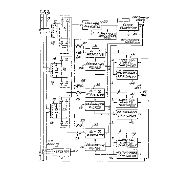
In FIG. 1 a normally closed three-pole/single-throw
switch 10 is arranged to interrupt conduction through each of
the conductors 11, 12 and 13 supplying phases ~A, ~B,
- 2b -
RD-19470
and ~C respectively in a three-phase power line. This inter-
ruption is controlled by an electrically tripped electrome-
chanical actuator 47 and occurs responsive to an overcurrent
condition being sensed as occurring in one or more of the
conductors 11, 12 and 13. The source sides of conductors 11,
12 and 13 can be at the top of FIGURE 1 and their load sides
at the bottom of FIGURE 1. Alternatively, the source sides
of conductors 11, 12 and 13 can be at the bottom of FIGURE 1
and their load sides at the top of FIGURE 1.
Current transformers 14, 15 and 16 have respective
primary windings included in conductors 11, 12 and 13,
respectively, and have secondary windings across which volt-
ages appear responsive to current flows through their primary
windings. The secondary windings of current transformers 14,
15 and 16 are shown with respective avalanche-diode overvolt-
age protectors 17, 18 and 19. The secondary windings of cur-
rent transformers 14, 15 and 16 supply their alternating
voltages to full-wave-rectifier diode bridges 21, 22 and 23.
The positive output voltages of these full-wave rectifier
diode bridges 21, 22 and 23 supply a voltage regulator 20
(which may be a shunt regulated type, for example) that sup-
plies a positive, regulated voltage to the electronic cir-
cuitry in the FIGURE 1 electronic circuit breaker.
The negative output voltages of these full-wave
rectifier diode bridges 21, 22 and 23 are applied via resis-
tors 24, ~5 and 26 respectively to the input ports of over-
sampled ~-~ modulators 31, 32 and 33 respectively. The regu-
lated positive voltage from voltage regulator 20 is alsoapplied to the input ports of ~-~ modulators 31, 32 and 33
via resistors 27, 28 and 29,. respectively, to bring the rec-
tified voltage swings within the analog-to-digital conversion
range of the ~-~ modulators 31, 32 and 33. This procedure
and the specific construction of a ~-~ modulator are more
particularly described by S.E. Noujaim in U.S. patent No.
20(~597
RD-19470
4,758,018 issued 30 August 1988, entitled "ANALOG TO DIGITAL
CONVERTER FOR AN ELECTRONIC CIRCUIT BREAKER WITH OUT-OF-
SUPPLY-RANGE INPUT SIGNALS" and incorporated herein by refer-
ence.
A clock generator 30 powered by regulated positive
voltage from voltage regulator 20 includes a crystal oscilla-
tor to generate a master clock frequency. Digital counters
count down from this master frequency to generate the over-
sampling clock signal for the ~-~ modulators 31, 32 and 33
and an analog-to-digital (ADC) sample clock. The ADC sample
clock can be a bit serial clock comprising a bit rate and a
word rate clock supplied on separate lines. By way of exam-
ple, electronic circuit breakers de-qigned by the inventors
have used a 3.56352 MHz oversampling clock signal rate and
decimation filters having a 28 decimation factor. Accord-
ingly, the word rate clock is 13.92 kHz in such a design. A
bit serial word of 25 bits has been used in the design, so
the bit-serial speed of operation is 445.44 kHz, supposing
there is no time-division multiplexing of digital hardware.
The digital samples from decimation filters 34, 35
and 36 are supplied to short-time-constant/long-time constant
trip signal generating circuits 41, 42 and 43, respectively,
as well as to instantaneous trip circuits 44, 45 and 46,
respectively. An OR gate 40 responds to a trip signal sup-
plied from any of the circuits 41-46 to forward that trip
signal to the electromechanical actuator 47 for causing the
normally closed three-pole/single-throw switch 10 to open and
interrupt conduction through each of conductors 11, 12 and
13.
FIGURE 2 shows more particularly how circuits 41
and 44 (or 42, and 45, or 43 and 46) appear. A user-set
threshold value supply supplies three threshold values. A
first of these three user-set threshold values is used in
-4-
2Q~gS97
RD-19470
developing the short-time-constant trip signals in circuits
41-43. A second of these three user-set threshold values is
used in developing the long-time-constant trip signals in
circuits 41-43. And a third of these three user-set thresh-
old values is used in developing the instantaneous trip sig-
nals in circuits 44-46. The first of these threshold values
is normally larger than the second, (e.g., by six times); and
the third of these threshold values is not only normally
greater than the second (e.g., by twenty times) but also is
greater than the first.
The signal from decimation filter 34 is supplied as
both multiplier and multiplicand to a digital multiplier 410
for squaring each sample of that signal. The squared samples
are supplied to an integrator 411 with fifty millisecond time
constant, which may for example be an averager for each
sequence of 696 samples at 13.92 KHz word rate. The fifty
millisecond integration time corresponds to 2.5 cycles of 50
Hz current, three cycles of 60 ~z current and twenty cycles
of 400 Hz current.
Relatively small groups of sequential samples (e.g.
twenty in number) are accumulated in an accumulator 412, and
the accumulation results are compared in a differential com-
parator 413 against the first threshold value from supply 50.
If and only if the accumulation results exceed the first
threshold value does comparator 413 deliver a logic ONE to OR
gate 416 and thence to OR gate 40, which ONE is the short-
time-constant trip signal. If its accumulation results do
not exceed the first threshold value from supply 50, compara-
tor 413 output signal is a logic ZERO.
Relatively large groups of sequential samples (e.g,
one-hundred-thirty in number) are accumulated in an accumula-
tor 414, and the accumulation results are compared in a dif-
ferential comparator 415 against the second threshold value
'~ 2~ 97
.
RD-19470
from supply 50. If and only if the accumulation results
exceed the second threshold value, does comparator 415
deliver a logic ONE to OR gate 416 and thence to OR gate 40,
which ONE is the long-time-constant trip signal. If its
accumulation results do not exceed the second threshold value
from supply 50, comparator 415 output signal is a logic ZERO.
Instantaneous trip circuit 44 compares signal from
decimation filter 34 with the third threshold value in dif-
ferential comparator 440. There are no delays in making this
comparison as would be caused by squaring, integration, or
accumulation. To lessen the chance of a one-sample transient
pulse condition causing a false trigger a short-pulse sup-
pressor 441 follows differential comparator 440. Each com-
parison result is ANDed in an AND gate 442 with its predeces-
sor, as temporarily stored in a clocked latch 443. AND gate442 response is logic ZERO unless any two successive digital
samples from decimation filter 34 exceed the third threshold
value, which exceptional condition causes AND gate 442
response to be a logic ONE. This logic ONE is the instanta-
neous trip signal, which is supplied to OR gate 40. Somevariation in the short-pulse suppressor is possible, (e.g.,
ANDing of three successive comparator 440 results may be done
to provide short-pulse suppression still less likely to gen-
erate false trip signals, at some sacrifice in speed of
instant trip response).
One skilled in the art and acquainted with the
foregoing disclosure will be enabled to design other embodi-
ments of the inventi~n, and this should be borne in mind when
construing the scope of the ensuing claims. For example,
electronic circuit breakers for protecting power lines with
any number of phases of alternating current and any number of
conductors can be constructed in accordance with the inven-
tion. Electronic circuit breakers for power lines transmit-
ting direct current can also be constructed in accordance
2(~09~St7
.
RD-19470
with the invention, by using a chopper in the connections to
the primary winding of each current transformer.
.