Note: Descriptions are shown in the official language in which they were submitted.
PHN 12 849 1 11-5-1939
Power-supply circuit.
The invention relates to a po~er-~upp.ly circuit for
charging a battery with a charging current, co~pri~ing between a first
and a second power supply terminal a first s~ries arrangement of a
primary winding of a transformer, a first trans.istor switch having a
S control input, a first resistor, and a second series arrangement of a
secondary winding and a irst diode, which second series arrangement ~-~
comprises terminals for the connection of a battery, a positive-feedback
path between the node the secondary winding and the fixst diode and the
control input of the fir~t transistor switch, which posltive-feedback
path co~prises the series arrangement of a second resistor and a first
capacitor, the terminal of the first capacitor which is remote rom the
second resistor being coupled to the cathode of a %ener diode, ~irst
switching Deans for turning off ~he Pirst tra~sistor switch at a
; specific voltage across the first resistor, which first switching ~eans
comprise a first inputcoupled to that end of the iirst resistor which is
nearest the first transistor switch, a ~econd input coupled to that end ~:
of the first resistor remote from the first ~ransistor switch, and an
output which is coupled to the control input of the first transistor
sNitch, and second switching means for changing over fro~ the charging
current to a trickle-charging current above a specific thre~hold
voltage.
Such a circuit can be e~ployed for exciting a battery
and/or powering a load with an input volta~e which ~ay be either ~:
rectified an alternating voltage or a direct voltage. In particular such
a circuit i5 suitable for use in a shaver for charging the battery
and/or powering the ~otor.
A power supply circuit of the type defined in the opening
paragraph is known fro~ European Patent Application 0,226,253. In this
circuit a current flows through the primary winding during the so-called ::;forward in~erval, as a result of ~hich energy is stored in the
transfor~er. The pri~ary current is coDverted into a voltage across a
resistor. ~hen a specific value of this voltage is reached the first
,' ~: "
: .~
P~N 12 849 2 11-5-1989
switching oeans turn off the first transistor switch, cau~ing the
primary current to be interrupted. The stored energy is then supplied to
the battery as a linearly decreasing charging current via the secondary
winding and the first diode during the so-called flyback intexval. After
the flyback the next ~orward interval is started by the positive
feedback betw~en the secondary winding and the control input of the
first switch. In this way the battery can be charqed comparatively
rapidly ~ith a comparatively large current.
In order to prevent the battery Prom being daMaged by
overcharging the known power supply circuit co~prises second switching
~eans ~hich turn o~f the power supply circuit via the first switching
~eans if the battery voltage exceeds a threshold value and which
subsequently render the circuit operative at the instant at which the
battery voltage has dropped below a ~pecific second value. As a result
of this the circuit is switched fro~ charging to trickle charging when
the threshold value is exceeded first ti~e.
However, the second switching Ineans in the prior art
power supply circuit comprise a comparatively large number of
co~ponents, which renders the circuit more susceptible to component
tolerances.
Therefore, it is an object of the invention to provide a
power supply circuit comprising simple switching ~eans for changing over
to a trickle charging ~ode. In accordance with the invention a power-
supply circuit of the type defined in the opening paragraph is
character.ized in that the anode of the zener diode is coupled to one end
of the first resistor, and in that the second switching ~eans comprise a
series arrange~ent of a third resistor, a second transistor switch
having a control input, and a fourth resistor, arranged between the
first input of the s~itchin~ amplifier and the second power supply
terminal, the control input of the second transistor switch being
coupled to the node between the second resistor and the first capacitor,
a third diode being arranged in parallel with the second resistor.
The additional components in the circuit required in the circuit ~or the
second switching ~eans co~prise only three resistors and one transistor,
which ~akes the power-supply circuit in accordance with the invention
si~ple to realise. ~he voltage ~hich appears across the capacitor during
the flyback and which is proportional ~o the battery voltage at ~he end
. '.
, .
7:3~3
PHN 12 849 3 11-5-1989
of the flyback turns on the second transistor s~itch at the en~ of the
flyback. In the case of a fully charged battery the fraction of the
battery voltage appearing across the third resistor is large enough to
energise the first ~witching means and conse~uently inhibit the next
forward interval until the voltage across the first capacitor has
decreased to such a value that the voltage across the third resistor is
no longer adequate to keep the first switching means energised. In this
way a number of for~ard intervals are inhibited after a flyback, causing
the average charging current to decrease and causing the circuit to be
changed over from the nor~al char~ing mode to a trickle charging mode.
The voltage at which the change over from nor~al charging
to trickle-charging is effected can be ~elected in such a ~ay that it is
equal to the motor voltage of a ~otor which can be connected in parallel
with the ~attery by ~eans of a switch. ~he power-supply circuit then
constitutes a constant-voltage source which, depending on the ~otor
load, is capable of supplying a current varying fro~ the trickle-
charging current to the nor~al charging current. The circuit in
accordance with the invention responds very rapidly to loacl changes,
so that the motor speed re~ains constant and load-independent.
A first embodiment of a po~er-~upply circuit in
accordance with the invention ~ay be characterized in that a power-
supply circuit as claimed in Claim 1 or 2, characterized in that a
series arrangement of a fifth and a sixth resistor is arranged between ?
the second input of the switching amplifier and the node between the
second resistor and the first capacitor, the control input of the
second transistor switch being connected to the node between the fifth
and the sixth resistor, the fifth resistor being suitably a variable
resistor. The voltage at which the second transistor switch is turned on
can be defined accurately by ~eans of the fifth and the sixth resistor.
A second embodiment of a power-supply circuit in
- accordance ~ith the invention is characterized in that the fourth
resistor is formed by the series arrangement of t~o resistors, whose
node is coupled, y~ a seventh resistorl to a control input for
receiving a control signal for increasing the vol~age at which the
change-over fram the nor~al charging current to the trickle-charging
curxen~ is effected. This enables a discharged ~attery to be rapidly re-
charged. This embodiment ~ay ~e characterized further in that, in order
,
~3~
PHN 12 849 4 11-5-1989
to increase the tuxn-of voltage, the seventh transistor is coupled to
the positive battery ter~inal, or in accordance with another e~bodiment
in that the node between the t~o resistors i5 connected to the base of a
third transistor, which h~s its collector and e~mitter coup}ed to those
ends of the two resistors which are remo~e fro~ the node, and in that,
in order to increase the turn-off voltage,~he Qseventh resistor is
coupled to the emitte~ of the third transistor.
A third e~bodiment of a power-supply circuit in
accordance with the invention i5 characterized in that the 3econd input
of the switching a~plifier i5 coupled to that end of the first resistor
which is re~ote fro~ the first transistor switch by means of a voltage
source for supplying a reference voltage which decreases as the input
voltage increases. These steps prevent the output current of the power
supply circuit from increasing when the input voltage increases as a
result of the increasing switching frequency.
A fourth embodi~ent of a power-supply circuit in
accordance with the invention is characterized in that the first
sNitching means co~prise a fifth transistor having its emitter connected
to the first input, having its base connected to the second input and
having its collector connected to the second power supply terminal by
~eans of a series arrangement of an eleventh and a twelfth resistor, the
node between the eleventh and the twelfth resis~or being connected to
the base of the sixth transistor, whose collector is coupled to the
control input of the first transistor switch and, YL~ a second
~: 25 capacitor, to the second input of the first switching ~eans.
The invention will now be descxibed in ~ore detail, by
way of example, with reference to the accompanying dra~ings in which
Fig. 1 shows a first embodiment vf A power-supply circuit
in accordance with the invention,
Fig. 2 shows some characteristic curves to illustrate the
operation of the circuit shown in Fig. 1,
Fig. 3 shows a second embodiment of a powex supply
circuit in ~ccordance with the in~ention,
Fig. ~ shows a third embodi~ent of a pswer ~upply circuit
in accordance with the invention, and
Fig. S shows a fourth embodiment of a power supply
circuit in accordance with the invention.
' ~
"
.
~ .
zuq9~38
PHN 12 849 5 11-5-1989
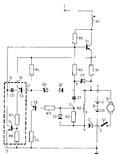
Fig. 1 shows the circuit diagram of a first embodiment of
a power-supply circuit in accor~ance with the invention. The circuit
comprises two input terminals 1 and 2 for receiving an input voltage,
which may be a rectified alternating voltage or a direct voltage.
Arranged between the terminal~ 1 and 2 is the ~;eri~s arrange~ent of the
primary winding n1 of a transformer, the collector e~itter path of a
transistor T1, a rasistor R1 and the series arrangement of a secondary
winding n2 and a rectifier diode D1. A battery B is connected between
the ter~inals 4 and 2 and in the present case 1:he battery is ormed by
the series arrangement o~ two nickel-cad~ium cells ~ and 10. A ~otor M
of, for example, a shaver can be connected in parallel with the battery
~ by means of a switch S1. The series arrangement of a resistox R2, a
: capacitor C1 and a resistor R3 is arranqed bet~ee~ the node 5 between
the secondary winding n2 and diode D1 and the base of the transistor
~1. A zener diode D2 is arranged between the node 7 of the capacitor Cl
and the resistor R3 and that end of the resistor R1 nearest the
terminal 4. The base of the transistor T1 is connected to the collector
of the transistor T1 by means of a starting res.istor R6. It is to be
noted that this resistor may alternatively be connected to the input
terminal 1. The ends 3 and 4 of the resistor R1 are connected to the
inputs 16 and 17 of first switching means 15, which have an output 13
connected to the base of the transistor T1. In the present example the
switching ~eans 15 comprise a transistor T3, having its e~itter coupled
to the input 16, having its base coupled to the input 17 and having its
collector coupled to the second power-supply ter~inal 2, ~1~ the series
arrange~ent of two resistors R7 and R8. The node between these two
resistors is coupled to the base of a transistor T4, having its emitter
coupled to the second power-supply terminal and having its collector
coupled both to the output 18 and, Yl~ a capacitor C2, to the input 17.
The transistors T3 and T4 together with the resistor~ R7 and R8 and the
capacitor C2 constitute a dynamic Schmitt-trigger circuit. The series
arrangement of a resistor R4, the collector-emitter path of a transistor
T2 and a resistor R5 is axranged between the first input 16 and the
power-supply terminal 2. The transis~or T2 has its base connected to the
node 6 between the resistor R2 and the capacitor C1. A diode D3 is
arranged in parallel with the resistor R2. The e~itter of the transistox
T2 is connected to the end 4 of the resistor R1 by ~eans of a zener
. . . : ~
.
. .
,, ' ' ' ' : ' '-
~ ' ~
;Z~73~ ~
P~N 12 849 6 11-5-1989
diode D4. A diode D4 is arranged in series with the ~ener diode D4, the
two anodes or the cathodes facing one another.
The operation of the circuit can be explained as follows
if, for the ti~e being, the effect of the trans:istor T2, the resistor R5
S and the diode D3 is ignored. It is assumed that the s~itch S1 is open
and the circuit only supplies the charging curr~nt for the cell~ 9 and
10. ~hen an input vol~age is present across the ter~inal3 1 and 2 a
s~all current will flo~ into the base of the transistor T1 ~ the
starting resistor R6, so that said transistor i~i driven partly into
conduction. The resulting curren~ through the pximary winding n1 results
in a voltage i~crease across the secondary winding n2, so that the
transistor ~1 is driven further into conduction as a resuIt of the
~ positive feedback ~L~ the resistor R2, the capacitor C1 and the resistor
; R3. As a result of the continuing positive feedback the tra~sistor T1 is
~5 rapidly saturated. The voltage across the secondary winding n2 is
; proportional to the voltage across the pri~ary winding n1 and hence to
the input voltage. The base current of the transistor T1 would therefore
be independent of the input voltage. This would result in an increasing
turn-off delay of the transistor T1 arise in the case of an
increasing input voltage, which would lead to an undesirable increase of
the charging cur~ent of the battery B. However, the base current o~
the transistor T1 produces such a voltage drop across ~he resistor R2
that the voltage on the node 7 reaches the breakdown voltage of the
zener diode D2. As a result of this the base current of the tra~sistor
T1 becomes independent of th~ input voltage, 50 that everytime the
transistor T1 is satura~ed to the sa~e extent and the turn-off delay is
consequently independent of the input voltage. The value of the base
current is defined by ~eans of the resistor R3. Alternatively, the anode
of the zener diode D2 ~ay be coupled directly to the e~itter of the
first transistor T1. However, the confiquration in Fig. 1 has the
advantage that the base current for the transistor at the beginning of
the forward interval is larger, so that the transistor ~1 is turned on
hard and the forward interval is started rapidly. ~oreover, in the 2bove
configuration the transistor T1 is driven less far into saturation at
the end of the forward interval, so that this transistor is cut off ~ore
rapidly.
Aftex the ~ransistor T1 is botto~ed as described above
:.; ~ ' '
.
200~3~3
PHN 12 849 7 11-5-1989
the current through the primary ~inding n1 incxeases as a linear
function of time during the forward interval. During the forward
interval the voltage on the node S i5 positive, ~o that the diode D1 is
cut off. The primary current is converted into a voltage across the
S resistor Rl, which voltage is applied to the series arrange~ent of the
base-e~itter junction of the ~ransistor T3 and the zener diode D4. When
the breakdown voltage of the zener diode D4 is reached the voltage on
the base 17 of the transistor T3 is ~aintained constant. ~s the primary
current increases further the voltage across the resistor R4 will
tO increase until the threshold voltage of the transistor T3 is reached and
the transistor T3 i5 turned o~. The collector current of the transistor
T3 drives the tra~sistor T4 into conduction YL~ the resistors R7 and R8,
so that base current i5 withdrawn fro~ the transistor T1. The ~oltage
step appearing on the collector of the transistor T4 is transferred to
the base of the transistor T3 y~ the capacitor C2, so that the last~-
mentioned transistor is rapidly driven into full conduction.
Consequently, the transistor T3 is turned on hard and the transistor T1
is cutt off rapidly.
Since there is no pri~ary current the polarity of the
voltage across the secondary windiny n2 is reversed, so that the diode
D1 is turned on. The energy stored in the trans~ormer during the forward ~-
interval is then supplied to the battery B in the form of a charging
current during the so-called fIyback. This current decreases to ~ero AS ~ ~:a linear function of time. During the flyback the voltage on the end 5
25 of the secondary winding n2 is negative and equal to the voltage across
the diode D1. At the end of the flybac~ the voltage across the winding
n2 becomes ~ero volts, so that the voltage on the node 5 bero~es equal
to the battery voltage. This positive voltage step on the node 5 ensures
that after some time the next for~ard interval is started ti~e owing to
the positive feed~ack via ~2l C1 and R3.
In the ~anner described above the cells g and 10 can be
charged co~paratively rapidly with a co~paratively large current, for
example a 2C current of substantially 1.2 A in the case of two 1C NiCd
rechargeable cells of 1.2 V each.
In order to prevent the cells 9 and 10 from being damaged
as a result o overcharging the power-supply circuit is provided with
very si~ple switching meansl which effec~ the change over from a nor~al
.
.
,,
38
P~N 12 B49 8 11-5-1989
charging current to a trickle-charging current as the cells are
r~aching the fully charged condition. These s~itching ~eans comprise the
transistor T2, the resistors R4, R5 and R11, the diode D3 together with
the resi~tor R2, the capacitor C1 and the zetler diode D2. The switching
5 ~eans operate as follows.
~ hen the cells 9 and 10 are being charged the voltage on
the emitter of the transistor T3 i~ at least equal to the battery
voltage during the forward interval~ The voltaçle on the base of the
transistor T2 is equal to the su~ of the battery voltage, the breakdown
voltage of the æener diode D2 and the voltage across the capacitor C1,
~hose terminal 6, which is situated nearest the ter~inal 5 of the
winding n2 which is positive during the for~arcl interval, is positive
relatiYe to the terminal 7. Therefore, the sum of the e~itter-base
voltages of the transistors T3 and T2 is negative, so that the
transistor T2 is cut off during the forward interval, Since .in this
situation no current flows into the base of the transistor T2, there
will be no voltage drop across R11. At the beginning of the 1yback the
polarity of the voltage across the secondary winding n2 is reversed, 30
that the diode D1 is turned on and the voltage on the node 5 becomes
equal to the negative supply voltage ~earth) minus one diode vo~tage.
As a result of this the capacitor C1 is re-charged via
the zener diode D2 and the diode D3. The voltage on the node 6, which is
coupled to the base of the transistor T2 y~ the resistor R11, is
thexefore zero volts. The voltage on the terminal 7 of the capacitor C1
25 i5 clamped at a value equal to the bat~ery voltage ~inus one diode
voltage by means of the zener diode D2 which is operated as a diode
durin~ the flyback, The voltage on the emitter 16 of the transistor T3
is equal to the battery voltage. The voltage difference between the
emitter 16 of the transistor T3 and the node 6 is the~ equal to the
battery vol~age. The resistor R11 now functions as a current~ iting
resistor for the base current of the transistor T2, so that the sum of
the two base-emitter voltages cannot become too large. In particular at
the beginning of the flyback, the voltage across the battery is
substantially higher than the actual battery voltage as a result of the
voltage produced across the internal resistance of the battery by the
charging current. Vnder normal conditions the voltage across the base-
emitter junctions of the ~ransistors T~ and T3, a~ the beginning of the
1~73t~
PHN 12 fl49 9 11-5~1989
flyback, is therefore higher than two base-emitter voltages, 50 that the
transistors T2 and T3 will conduct. As long as the transistor T2 dra~s
e~ough current the .resistor ~4 will maintain an adequate base-e~itt~r
voltage across the txansistor T3 to keep this transi~tor T3 in the
conductive state and, Yl~ the transistor T2, the switching transistor T1
in the cut-off state. This prevents the transistor T1 from being turned
on again after turn-off.
In order to eli~inate the influence of the internal
resi~tance on the battery voltage, the detection whether the batteries
have been charged adequately and it is necessary to chanqe over to
tri~kle charging is effected by detecting the battery voltage at the end
of the flyback when the charging current is zero. At the end of the
flyback the voltage across the secondary winding n2 beco~es zero volts
and the voltage on the node 5 between the secondary winding and the
diode D1 jumps from zero volts to the battery voltage. Thi~ voltage
step i5 not follo~ed im~ediately by the node 6 between the capacitor C1
and the resistor R2, so that the voltaqe on the base of the transistor
T2 ~ill not change im~ediately at the end of the flyback. Consequently,
a voltage equal to the voltage across the capacitor C1 will appear
between the emitter of the transistor T3 and the base of the transistor
T2. During the flyhack said capacitor has been charged to the battery
voltage minus the voltage across the d.iode D2, so that the voltage
across this capacitor C1 is proportional to the battery voltage. When
the cells have been charged ade~uately the voltage across the
capacitox C1 will be so large that the transistors T2 and T3 conduct.
Since the zener diode D2 is operated as a diode and
remain~ conduct.ive, the voltage on that terminal of the capacitor C1
which is situated nearest ~he zener diode D2 remains equal to the
difference between the battery voltage and the volta~e across the ~ener
diode D2. As long as the switching transistor T1 remains off the node 5
will xe~ain at the battery voltage. The terminal of the capacitor C1
nearest ~aid nnde then gradually adopts this voltage, the ti~e constant
being dictated by the RC time of the circuit comprising R2 and C1. ~s
long as the voltage is sufficiently high the tranisstors T2 and T3
re~ain conductive. As a result of this the transis~or T1 remains cut
off, thereby inhibiting the start of the nex~ forward interval. The
transistor T2 i3 then ~aintained in conduction to a suitable extent. If
: . ,. : .
: .,
200~38
PHN 12 849 10 11-5 1989
the slight voltage drop across the resistor R1 and the collector-emitter
voltage across the transistor T2 are ignored the voltage across the
xesistors R4 and RS ~ill be equal to the battery voltage. The transistor
T3 then remains in the conductive state until the voltage across the
S capacitor C1 has decreased so far that the transistor T2 i5 cut off and
the voltage across the resistor R4 becomes too s~all to ~aintain
conduction of the transistor T3. The next forwilrd interval can then be
started. At least on~ base-emitter voltage re~ainx available on C1, so
that T1 is im~ediately driven into conduction at the beginning of the
forward intexval. Thus, when a specific battery voltage is reached and
the cells have been charged adequately a number of ~orward intervals
are inhibited after every forward interval, thereby reducing the average
charging current. In ~his way it is possible to change o~er, ~or
example, fro~ an 1.2 A charging current to a 0.12 A trickle-charging
current.
Fig. 2a shows diagrammatically the primary current in the
trickle-charging mode, the suppressed forward intervals being indicated
in broken lines. Fig. 2b shows diagrammatically the average charging
current as a function of the battery voltage.
In the circuit arrangement shown in Fig. 1 the change-
over point from the normal charging current to the trickle charging
current can be situated at any desired voltage, for examplel the ~otor
voltage. In that case the power-supply circuit will operate as a
constant-voltage source when the switch 51 is closed, ~hich source
depending on the load of the motor is capable o~ ~upplying an output
current ranging from ~he trickle charging current to the nor~al charging
current. This prevent the supply voltage of the motor and hence the
speed of the motor from increasing as the load increases.
The circuit described herein exhibits a steep dependence
hetween khe delivered current and the voltage, so that in the case of a
load variation of the motor the current supplied to the ootor varies
rapidly between 0.12 A and 1.2 A and the motor speed remains constant.
Fig. 3 shows a second embodi~ent of a powex-3upply
circuit in accordance with the invention. Identical parts bear the same
reference numerals as in Fig. 1. In this embodiment the ~ains voltage is
applied to a brid~e rectifier G via two terminals 20 and 21. The
rectified voltage is smoothed by means of a filter 22 co~prising a coil
.
Z~3,0~
PRN 12 849 11 11-5-1989
L1 and two capacitors C3 and C4 and i5 subsequently applied to an input
terminal 1. The ~eries arrangement of a zener diode D5 and diode D6 is
arranged in parallel with the pri~ary winding ~o ~uppre~ voltage suges
when the current through the primary ~inding is switched off.
S A voltage divider comprising the resistors R10 and R11 is
arranged between the emitter and the base of the tran~istor T2, the
resistor R10 being suitably a variable resistor. This voltage divider
enables the voltage at which the transistor T2 is driven into conduction
and hence the voltage at which the change-over from the normal charging
current to the trickle-charging current is effected to be adjusted
accurately.
~ oreover, the resistor R5 in the present e~bodi~ent is
split in~o t~o resistors R5a and ~5b, the node between tbese resistors
being connected to a control input 25 by means of a resistor ~12. ~hen
this input 25 is connected to the positive terminal of the bat~ery a
fraction of the battery voltage, ~or example half this voltage, will
appear across the resistor R12. ~hen khe transistor T2 is botto~ed
during the flyback the voltage divider co~prising the resistor R4 and
the resistor R5a then ensures that ~gain a fraction of the voltage
across the resistor R12 appears across the resistor R4. By suitably
dimensioning the resistors R4 and R5a the transistor T3 can be turned on
at 2 higher battery voltage than that at which the transistor T3 is
turned on in the absence of a signal on the signal input 25. This
changing over to the trickle-rharging current is possible at a higher
battexy voltage than during normal use. This possibility can be utilised
in order to recharge drained batteries very rapidly. Moreover, the
present embodi~ent comprises a light-e~itting diode D7 and a resistor R9
arranged in series between the positive terminal 4 of the battery and
the base of the transistor T1. In the charging mode the diode D7 will
blink at such a frequency that it gives the impression of a continuously
lit diode. The diode D7 thus functions as a ~attery charging indicator.
Fig. 4 shows a third e~bodiment of a power-supply circuit
in accordance with the invention, identical parts bearing the sa~e
reference numerals as in Fig. 3. The ra~e a~ which the pri~ary current
increases as a linear function of time during the forward interval is
proportional to the input voltage. For an increasing input voltage the
primary current value of which the transistor T1 is turned off i5
. ~
' ' " '. ',, ':
~ ,7~
PHN 12 84g 12 11-5-1989
therefore reached increasingly faster. This results in a higher
~witching frequency of the power supply circuit, as a result of which
the avera~e charging current increases when the input voltage increases.
In order to maintain the charging current constant as far as possible
when the input voltage increases the circuit is provided with input
voltage compensation. For this purpose the zener diode D4 of the circuit
shown in Fig. 3 is replaced by a reference-vol1:age circuit, whose
reference-voltage decreases as the input voltage increases. This
reference-voltage circuit co~prises a series arrangement of resistors
R13 and R14, which is arranged between the emitter of the transistor T2
and the end 4 of the resistor R1 and whose nod~ is connected to the
base of a transistor T6, having its collector connected to the resistor
R13, having its emitter connected to the resistor R14, and having its
base connected to the terminal 5 of the secondary winding n2 by means of
a resistor R15. During the forward interval a fraction of the voltage
across the resistor R1 appears across the resistor R14 v'a the voltage
divider R4, R13 and R14 and a fraction of the voltage across the
secondary winding n2 appears across this resistor R14 y~ the voltage
divider R15, R14. ~hen the voltage across the resistor R14 reaches the
threshold voltage of the transistor T6 this transistor i~s turned on. The
collector-emitter voltage is then equal to the base-emitter voltage of
the transistor T6 multiplied by a factor dictatea by the resistance
value of the resistors R13 and R14. This voltage does not increase any
further as the voltage across the resistor R1 increases. ~henthe input
voltage increases the voltage across the secondary winding n2 increases,
causing the voltage across the resistor R14 to increase. In this way it
is achieved that for an increasing input voltage the voltage across the
resistor R14 reaches the base emitter threshold voltage of the
transistor T6 at decreasing values of the primary current, so that for
an increasing input voltage the transistor T1 is turned off at
increasing values of the primary current. As a result of ~his, the
average output current of the circuit becomes substa~tially independe~t
of the input voltage.
Fig. 5 shows a fourth embodiment of a power supply
circuit in accordance with t~e invention, identical parts bearing the
same reference nu~erals as in Fig. 4. In this e~bodi~ent the resistor
R15 is not connected to the positive terminal of the secondary winding
!~38
PHN 12 ~49 13 11-5-1989
n2 during the forward interval but it is connected to the positive
terminal of the primary winding n1. It is to be noted that alternatively
the resistor R15 may be cvnnected to any other point in the circuit
which is at a voltage proportional to the input voltage. In the present
e~bodiment the node be~ween the resistors RSa alnd R5b is, ~oreoverl
connected to the base of a transistor T7 havincl its emitter connecte~ to
that end of the resistor RSb which is remote from the base and having
its collector connected to that end of the resi.stor R5a which is remote
from the base. ~oreover, the base of the transi.stor T7 is connected to
the control input 25 hy the resistor R12. ~hen the transistor T2 i5
conductive the voltage produced across the resistor RSb is higher than
the threshold voltage of the transistor T7, so that this transistor will
conduct. The collector-emitter voltage of this transistor is then fixed
at a value equal to the product of the base emitter voltage of the
1~ transistor T7 and a factor determined by the resistance values of the
resistors RSa and R5b. The difference between the battery voltage and
the voltage across the transistor T7 appears across the resistor R4 and
deter~ines whether a change over to trickle charging is to be effected.
By connecting the terminal 25 to the emitter of the transistor T7 the
resistors R5b and R12 are arranged in parallel. ~hen the value of the
resistor R12 is suitably selected relative to that of the resistor R5b
~he voltage across the transistox T7 is increased. This means that a
smaller portion of the battery voltage will appe~r across the resistor
R4 than in the case that the terminal 25 does not carry a signal. As a
result of this the battery voltage at which the change-over to trickle-
charging is effected will be higher than in the first-mentioned case.
The invention i5 not limited to the e~bodime~ts shown
herein. ~ithin the scope of the in~entions a variety of modifications
wil be conceivable to those skilled in the art. For example, the first
and the ~econd transistor switches may alternatively comprise compound
transistors or other semiconductor switch.ing elements. ~oreover, the
first switching means may be constructed in another way than shown and
the input voltage compensation means may also be constructed in another
way than shown.
, ", .
.