Note: Descriptions are shown in the official language in which they were submitted.
2~0313
~:
LIGHTING CONTROL SYSTEM
Background of the Invention
This invention is directed generally to the theatrical
and stage lighting arts, and more particularly to a
novel and improved lighting control system which may
advantageously be used in connection with the control
of stage or theatrical type lighting.
Stage and theatrical lighting systems generally make
use of a variety of lamp types which rec~uire a
corresponding variety of power sources for their
operation. Such systems or installations may include a
number of different types and kinds of lighting for use
at different times and/or i'or different applications.
Such lamps may include, for example, high pressure arc
lamps which require relatively high start-up voltages,
i.e., which may be from two to five times the lamp's
normal operating voltage~ depending on the particular
lamp characteristics. Such high pressure arc lamps
usually require a series ballast to reduce the voltage
at the lamp terminals.
Moreover, it is often desirable to provide light
dimming circuits for contrc,lling the intensity of lamps
--2--
26C~3~ 3
in such a stage or theatrical lighting system, either
individually or collectively, as desired.
Heretofore, electrical control systems for such
lighting installations have been relatively large and
cumbersome, requiring many large and relatively
expensive electrical components. This has been
necessary in order to accommodate the desired range of
control of operating voltages, dimming, and the like,
for a large number of lamps, which, as indicated above,
may have varying electrica:L operating requirements.
Moreover, it has heretofore been necessary to provide a
completely separate electrical control system in order
to change the operating line voltage, and often even in
order to operate at a different line frequency. That
is, for example, standard IJ.S. "house current" is 120
volts 60 hertz, whereas many European systems provide
220 volts 50 hertz current. Such lighting control
systems have further heretofore required relatively
large, heavy and cumbersome choke coils, transformers,
wire-wound rheostats, and t:he like to provide a desired
range of start-up and dimming controls for a large
number of lights in a given system or installation.
Moreover, such systems have heretofore generally been
incapable of operating different lamps which may be
used in such a lighting system or installation. For
example, lamps of 12 volts, 28 volts, 60 volts, so
volts or 120 volts may be selected for use in a given
system. Generally speaking, the lower voltage lamps
are less expensive and are often preferred by lighting
technicians. Moreover, wit;h systems heretofore in use,
lamp life is often unduly shortened, because of lack of
adequate control over the voltages and current supplied
to the lamps during operation. Also, in the case of
short circuits or overloading of the system, present
~&~323
control systems often fail to provide adequate
protection for the lighting equipment.
Importantly, our new lighting control circuit allows
the addition of dimmers for controlling a large number
of high wattage lamps either individually or
collectively, while avoiding much of the expensive and
cumbersome equipment associated with the prior art
dimmer and control systems. For example, early
versions of theatrical light dimmer systems involved
cabinets some eight feet tall, four feet deep and six
feet wide, weighing 1,000 pounds or more. These
systems were clearly not portable in nature, and
moreover usually offered a maximum of only 12 dimmer
controls. Moreover, these units operated only with 120
volt AC lamps and offered no flexibility whatever for
lamp interchangeability. More recent technology offers
more compact packages, on the order of only 12 to 20
inches in length, width and depth. However, such
controls generally weigh from 65 to 85 pounds for 12
dimmers. Moreover, these newer system still do not
permit lamp interchangeability, but are generally
designed to operate in connection with only one lamp
type.
Furthermore, the prior art systems generally did not
accommodate changes in lamps or operating voltages
because relatively heavy and expensive components such
as power SCRs and heavy-duty toroidal filters were
generally custom manufactured for operation with but a
single type of lamp and at a single voltage. Larger
dimmer systems generally were proportionately larger,
more complex and more expensive than the
above-mentioned 12 dimmer type of system. For example,
many installations, both permanent and portable,
require as many as from g6 to 200 dimmer modules or
2~0;~1 3
dimmer controls. SuCh systems, generally referred to
in the art as a "high density rack", are both heavy,
complex and expensive, and yet offer suprisingly little
flexibility in their operation. By way of example,
high density racks systems presently available do not
offer switchable lamp voltages or short circuit
protection. The approximate weight per dimmer control
of these systems runs from three to five pounds.
Noreover, such systems require a minimum of a 10 watt
load for safe operation and generally offer output
power at only 120 volts.
Obiects and SummarY of the Invention
Accordingly, it is a general object of this invention
to provide a novel and improved lighting and power
control circuit which generally overcomes the
above-noted shortcomings of the prior art systems.
A related object is to provide a control circuit in
accordance with the forego:ing object which may readily
be used with a number of different voltage lamps
without unnecessary duplication of complex and
expensive circuit component:s.
Another related object is t:o provide a control circuit
in accordance with the foregoing general object which
is capable of operating a lighting system on a wide
range of available power sources or "house currents",
without changing lamps, using expensive transformers,
or the like.
A further related object is to provide a control system
in accordance with the foregoing general object which
advantageously promotes longer lamp life and
automatically shuts down in the case of short circuit
7 ~
or overload cond~t,ions t;o protect tlle connt~cted light,ing
circuits.
A furt~er object. is to provide a controI circuit in
accordance with the foregoing qeneral obje,~t whlch is
considerably smaller in size and lighter ir weight. than prior
art systems.
The invention provides accorcIlrIg to one aspect a
lighting control ~-ircui1:; f'or iI.luminatlng and dlmming of a
least one light ln a light,ing c~ircult, sdic~ lighting control
circuit comprising: power supp1y means for recelving an AC
line voltage inpl~t, and f'or converting said AC l,Lne voltage to
selectable rect:ified AC and DC power sup~ es; t,iming
generator circuit means coupled with said power supply means
and responsive t( a rec1.,if.ied AC power supIly fronl said power
supply means for genera1:,ing and shapiny ar1 elect,rical timing
signal; timing rclopara-t(:)r circ~lit means re~pons-ve to said
electri~al timi.n<~ signal. and t::o a select.db~e contIol voltage
for generating a ~ariab:L.e duty ~-ycle O-ltpll~ siynal; switching
circuit means collpled w:i.th saic1 l.ighting c,rcuit. for gating
current therethrough and havin~ a contIol nput ccupled in
circuit with saic1 timing comparator CiI CU:it: means for gating
said current in accordallce with said vaIia},le duty cycle
output, and current lim:i.ti.ng comparatoI: CilCUit means coupled
with said switchir,g cir(:ui.t; means and wi.th said lighting
circuit means for compa]~irlg the current gated by said
switching circult means wi.t;h a selectable t.hreshol.d value and
for controlling sdid sw:i.tching circuit mears to limit current
flow in said light.ing c:i.rcuit ln ac(~ordal-c~ Wit]1 said comparison.
-- 5
76194-l
,~
3 ~.~
Accord]ng to ancther aspect. the invention provides
a lighting control clrcuit for controll.illg illumination and
dimming of at least one light :in a ]ightin~, clr~uit, said
lig:hting control -ircu:it. comprising: power supply means for
receiving an AC line vo].ta,ge irlput and for converting said AC
lin,e voltage to selecta~-le rectified AC ane DC power supplies;
timi.ng generator: il'CU.it:. nleans coupled with said power
supply means and respons.ive to a rectified AC power supply
from said power sl~pply mearls f)r gerlerat.Lng and shaping an
electrical timing signa1; t;iming compaI-atoJ cirluit means
responsive to sald elec1:rical t.iming si.gna' for generating a
variable duty cyele output signal; switchiJg cilcuit means
coupled with said light:incl circllit for gat-lng current
therethrough in accordallce with said variahle duty cycle
out~ut signal; and ~lne voltage i.so~ation ~ircu:it means
interposed betweer, said ti.ming compara1Or r ircit means and
.said switching C:i~C~Iit meclns for isolat.ing AC l:Lne-connected
circuit portions from lc)w-voltage cl.rcui.t p,orti~)nc;.
Accord:ing to yet; another aspect, the l.nvention
provides a light:ing cQn1rc)1 CiI-CUit for colltrol:lirlg
il].umination and dimnnint) of at least one l:ight i.n a lightin
circuit said lighting control ~ircu~t co~prisinq: power supply
means for receivi~g an AC line voltage i.np~t and for
converting said A~ line voltage to selecta}~le rectified AC and
DC power supplies; t..imil-1g generator circull means coupled with
said power suppl~ means and re.sponsive tn~ .l rectlfied AC power
supply from said power suE~ply means for generat:ing and shaping
an electrical tin,l.ng signal; timing comparat.or ~ircuit means
-- 5a -
iB 76194-l
~O/L) ~13
responslve to sald electri.cal tlmlng slgnal for generatlng a
varlable duty cycle output: slgnal; and swltchlng clrcult means
coupled wlth ~3ald llght:Lns~ clrcult for gating current
therethrough ln accordance wlth sald varlable duty cycle
output slgnal~ said swltchlng clrcult means lncludlng power
translstor means coupled ior gatlng current through sald
llghtlng clrcult and further lncludlng waveform shaplng
clrcult means coupled between sald tlmlng comparator clrcult
means and sald swltchlng clrcult means for regulatlng the
swltchlng tlme of sald power translstor means.
Brief DescrlPtlon of the I)rawlnqs
The fe~tures of the present inventlon whlch are
belleved to be novel are set forth wlth partlcularlty ln the
appended clalms. The organlzatlon and manner of operatlon of
the lnventlon, together w:lth further ob~ects and advantages
thereof, may best be understood
- 5b -
66382-199
2~313
by reference to the following description taken in
connection with the accompanying drawings in which like
reference numerals identify like elements, and in
which:
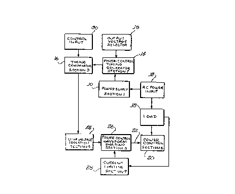
Fig. 1 is a schematic circuit illustration, in block
diagrammatic form, showing a lighting control circuit
in accordance with the present invention;
Fig. 2 is a schematic circuit diagram illustrating
details of a power supply section of the circuit of
Fig. l;
Fig. 3 is a schematic circuit diagram illustrating
details of a phase control timing generator section of
the circuit of Fig. l;
Fig. 4 is a schematic circuit diagram illustrating
details of timing comparator and line voltage isolation
sections of the circuit of Fig. 1;
Fig. 5 is a schematic circuit diagram illustrating
details of waveform shaping and power control sections
of the circuit of Fig. l; and
Fig. 6 is a schematic circuit diagram illustrating
details of a current limiting section of the circuit of
Fig. 1.
Detailed Description of the! Illustrated Embodiment
Turn:ing now to the drawings and initially to Fig. 1,
there is illustrated a lighting control circuit in
accordance with the invention, in block diagrammatic
form. As illustrated in Fig. 1, the lighting control
-7-
2G~0313
circuit in accordance with the invention includes a
power supply means or section 10. This power supply is
adapted for receiving an AC line voltage input for
example from an AC line or power input source 12 and
for converting this AC line voltage to selectable
rectified AC and DC power for delivery to the lighting
cont:rol circuit. A timing generator circuit means
(phase-control timing generator) 14 is coupled with the
power supply 10 and is responsive to a rectified AC
sample from the power supply for generating and shaping
an electrical timing signal.
A timing comparator circuit means 16 is coupled with
the timing generator circuit 14 and is responsive to
the electrical timing signal therefrom for generating a
variable duty cycle output signal. The lighting
circuit or load 18 is coupled between the AC power
source or input 12 and a power control circuit means or
section 20. This power control circuit 20 includes
switching circuit means coupled with the lighting
circuit or load 18 for gat:ing current therethrough. A
control input 22 of the circuit 20 is coupled in
circuit with the timing comparator circuit 16, by way
of intermediate circuits to be described later, for
gating the current through the load generally in
accordance with the variable duty cycle output of the
timing comparator circuit 16.
Preferably, the control circuit in accordance with the
invention also includes a ]ine voltage isolation means
or section 24. This isolation means 24 is interposed
between the timing comparat:or circuit 16 and the
switching circuit means of power control section 20 for
isolating the AC line connected circuit portions from
the :Low voltage circuit portions of the control circuit
or system. In the illustrated embodiment a further
power control or waveform shaping circuit means 26 is
2~)3~ ;~
also interposed between the timing comparator circuit
16 and switching circuit means of the power control
sect.ion 20. In the embodi:ment illustrated herein, this
power control or waveform shaping circuit section is
located subsequent to the .line voltage isolation
sect.ion 24. The waveform shaping circuit means 26
operates to regulate the s~itching time of the
switching circuit means.
Furt.her in accordance with the preferred form of the
invention illustrated here:in, a current limiting or
comparator circuit means or section 28 is also coupled
with the switching circuit means, and with the power
control waveform shaping c:ircuit 26. This current
limiting comparator circuit means or section 28
generally includes means for sensing the load current
through the load 18 and for comparing the load current,
as gated by the switching circuit means the power
control circuit 20, with a selectable threshold value.
The current limiting section and power control waveform
shaping section 28, 26 furt:her operate to control the
switching circuit means so as to limit current flow in
the load or lighting circuit in accordance with this
comparison.
Refe:rring now more particularly to the individual
functional blocks indicatecl in the diagram of Fig. 1,
the power supply section lt~ receives AC power and
produces DC voltages for the low voltage lighting and
control circuits as well ac; a sine wave AC sample for
the timing generator section 14. The power supply also
includes a high voltage D.C. supply for portions the
line--connected circuits and for the load. A full wave
rect:ified signal from the power supply is used to
synchronize operation of th.e phase-control timing
generator to the AC line vcl~ltage and to thereby shape
9 2~0313
the timing signal so that its DC voltage at any time
cor~.esponds generally to the RMS voltage of the AC line
volt:age.
The timing signal, preferably in the form of a ramp, is
fed to the timing comparator circuit 16. The
comparator compares the timing ramp signal from the
phase-control timing generator 14 to a control voltage
generated at ~ control input 30 to thereby generate a
vari.able duty cycle square wave control signal. The
line voltage isolation circuit means 24 feeds this
variable duty cycle square wave through to the
following circuitry while isolating these low voltage
circuits from the line-connected circuits.
Accordingly, an output square wave which corresponds to
the input variable duty cycle square wave is fed to the
power control waveform shaping circuit 26. The square
wave signal is altered by the circuit 26 to control the
switching time of the powex control section 20.
Accordingly, the power control section 20 acts as a
switching circuit or gating circuit so as to gate or
control the flow of currenl: through the lighting
circuit or load 18.
Advantageously, as will be more fully explained
hereinbelow, the rate of change of the control voltage
is limited, so that the load current does not change
rapidly enough to cause int:erference and distortion on
the AC power line. Moreover, the load current is
sampled and fed to the current limiting section 28,
wherein it is compared to a. selected threshold value.
If this threshold is exceeded, a latch is set for the
duration of the half-cycle to prevent further current
flow in the power control circuit 20. The output of
this latch is then fed to waveform shaping circuit 26
so as to effectively cut off the power control circuit
20, t:hus
- -10-
2~3~3
shutting off current flow in the load or lighting
circuits 18.
Reference is now invited to Figs. 2 through 6, in
connection with which, a more detailed description of
the construction and operation of the circuits of Fig.
1 wiLll be given.
Referring initially to Fig. 2, the power supply section
(sec-tion 1) receives AC power from the AC power input
12 which may be, for example, a 120 volt AC, 60 hertz
"household" current source. Preferably the current is
passed through a circuit breaker 210 which will open in
the case of overload anywhere in the non-isolated
portion of the circuit. The AC current is then
rectified by a diode bridge 212 to provide a 120 volt
DC source 214, part of which passes through a voltage
divider made up of resistors 216 and 218 and a diode
220 to make up a 15 volt (B) DC source 222.
Preferably, this 15 volt source 222 is regulated by a
zener diode 224 and a filter capacitor 226. It should
be noted that connection of resistor 218 to ground
assures that the 120 volt l)C source will drop to zero
volts DC during the zero crossing of each half cycle of
the ~C power source.
Part of the AC current from the power source 12 also
flow~ through a fuse 228 to the primary winding 230 of
a tr;~nsformer 232, which converts the voltage to 24
volt; AC, with a center tap connected as isolated
common in the secondary winding 234. Part of the
current from the secondary 234 is rectified by diodes
236, 238, filtered by resistor 240 and capacitor 242
and regulated by zener diode 244 to provide a positive
15 volt(A) source 245. The secondary coil 234 also
provides a current which is rectified by diodes 246,
- 1 1 -
2G10313
248 filtered by resistor 250 and capacitor 252 and
- regulated by zener diode 254 to form a negative 5 volt
source 255. A final part of the secondary current in
secondary coil 234 is rectified by diodes 256 and 258
to provide a rectified sine wave source 265 across
resistor 260. The respective voltage sources provided
by t:he power supply of Fig. 2 are utilized at various
supply points in the ensuing circuits as indicated in
the respective circuit diagrams.
Fig. 3 comprises a detailed schematic circuit diagram
of t:he phase-control timing generator 14 (section 2) of
Fig. 1. Referring now to Fig. 3, the rectified sine
wave sample from source 265 passes through a resistor
310 to the inverting input of an operational amplifier
312 where it is inverted and amplified by the ratio of
the values of resistors 31l0 and 314 and level-shifted
by the voltage divider consisting of resistors 316
318. The output of the op amp 312 is summed and
integrated with the output of a variable voltage
divider made up of resistors 320 and 322 by capacitor
325 and operational amplif:ier 335. The output of op
amp 312 is fed through a variable voltage divider made
up of respective variable resistors 320 and 322.
The recitifed sine wave sample also passes through an
isolation resistor 324 to 1;he inverting input of a
further operational amplifier 326 where it is compared
to a percentage of the 15 volt(A) voltage divided by
resistors 328, 330, the junction of which is coupled to
the non-inverting input of a comparator 326. The
output of comparator 326 will be low except at the
half-cycle zero-crossing~point when it will go
positive and pass through resistor 332 to turn on the
base of transistor 334. This will in turn discharge
the capacitor 325 and reset the phase-control timing
2~:310313
signal which is produced at the output of op amp 335.
It should be noted that the phase control timing
signal thus forms a constantly rising ramp-type signal
whic:h will ramp up until it either reaches the
positive supply rail or is reset by the turn-on of
resistor 334 as described above.
Reference is invited next to Fig. 4, wherein the
details of the timing comparator 16 (section 3) and
line voltage isolation 24 (section 4) circuits is
shown. It should be noted at this point that the
portion of the circuit of Fig. 3 enclosed in dashed
line may be repeated as many times as desired to form
a plurality of phase control timing ramps at different
output voltage levels, as desired. Accordingly, and
turning again to Fig. 4, an output voltage selector,
indicated by reference numeral 15 in Fig. 1, comprises
a multiple position switch 410, which in Fig. 3 has
been illustrated as a three position single pole
switch. Three selectable voltage timing ramps are
illustrated, by way of example, as being 12 volt and
120 volt.
However more or fewer such selectable voltages at any
desired value may be selected and provided in the
manner illustrated and described above with reference
to Fig. 2, without departing from the invention.
Accordingly, the circuit portion within the dashed line in
3 may be duplicated as many times as desired to produce a
desired number of repeating ramp or "saw tooth" output
signals, each of which corresponds to a different
selectable output voltage at the load 18. Accordingly,
switch 410 selects one of these timing ramps or saw
tooth signals which then passes through an isolation
resistor 412 to the inverting input of a comparator
2~03~3
414. The selected ramp is compared to a selectable
control voltage which is provided at the control input
30, which corresponds to control input 30 of Fig. 1.
This control voltage may be supplied by low voltage
wiring from a remote location, if desired. The output
of comparator 414 is a variable duty cycle square wave
which passes through a current limiting resistor 416 to
an optical isolator circuit 418 which comprises the
line voltage isolation circuit 24 (section 4). This
energizes an internal LED of the optical isolator 418
which in turn turns on an internal phototransistor so
as to draw a current from the 15 volt(B) source through
a resistor 420. This in turn pulls up the phase
control square wave output 422. Part of the current is
passed back through resistor 424 to stabilize the
internal phototransistor of the optical isolator 418.
This phase control square wave passes through an RC
filter composed of resistors 510, S12, variable
resistor 514 and capacitor S16 (see Fig. 5). This RC
filter alters the rise and fall times of the square
wave which is then fed through respective isolation
resistors 518, 520 and 522 to the respective gates of
power transistors 524, 526 and 528. This in turn
limits the rate of current change through the power
transistors which reduces t:he distortion imposed on the
AC line voltage and eliminates the need for an
inductive filter choke in series with the load. The
load current passes through a resistor 530 which
converts the load current to a small sample voltage
("load current sample") at a sample point 532. The
circuit of Fig. 5 thus comprises the power control wave
form shaping circuit 26 (section 5) and power control
circuit 20 (section 6) of the circuit of Fig. 1.
Turning next to Fig. 6, the current limiting circuit 28
~ -14-
2010313
~ (section 7) of Fig. 1 is i.llustrated. The load current
sample from sample point 5~32 is introduced through an
isolation resistor 710 to the non-inverting input of an
operational amplifier 712 where it is inverted and
amplified by the ratio of values of resistor 714 to
resistors 716 and 718, the latter being a variable
resistor so as to provide a wide range of
amplification. The amplified and inverted voltage is
passed through a further isolation resistor 720 to the
non--inverting input of a comparator 722 where it is
compared to a threshold voltage, set by a voltage
divider comprising resistors 724 and 726 and filtered
by resistor 728 and capacitor 730.
Accordingly, if the current exceeds the threshold
value, the output of comparator 722 swings high and
passes through diode 732 which in turn charges
capa.citor 734. This also swings the output of a
following comparator 736 negative and, through output
diod.e 738 overrides the phase control square wave and
swit.ches off the power transistors 524, 526 and 528
immediately. This in turn drops the load current to
zero and changes the output of comparator 722 back to
low. However, diode 732 allows capacitor 734 to retain
its charge and keep the flow of current switched off.
In order to allow conduction during the next
half-cycle, the full-wave rectified AC voltage (120 VDC
source) is introduced by way of a voltage divider
comprising resistors 740 and 742 and a current limiting
resistor 744 to the non-inverting input of a comparator
746. There, the divided voltage is compared to a
port.ion of the 15 volt(B) source voltage which
proportion is set by voltage divider 748, 750. The
OUtpllt of comparator 746 wi.ll swing negative during the
zero crossing of the AC vol.tage and discharge the
-15-
,; 2~10313
capacitor 734 through diocle 752 and resistor 754.
It will be apreciated from the foregoing description
that the novel lighting control system of the invention
permits use of a relative]y simple, low-voltage
electronic circuit which may be readily configured to
accommodate any desired number of output voltage levels
for various lighting circuits or other loads. The
number and values of the output voltages may be varied
as desired, as noted above, by the selection of the
numher and voltage levels of the relatively simple and
eas:ily duplicated circuit portion as indicated in
dashed line in Fig. 3, as noted above.
While particular embodiments of the invention have been
shown and described in detail, it will be obvious to
those skilled in the art that changes and modifications
of t:he present invention, in its various aspects, may
be made without departing from the invention in its
broader aspects, some of which changes and
modifications being matters of routine engineering or
design, and others being apparent only after study. As
such, the scope of the invention should not be limited
by t:he particular embodiment and specific construction
described herein but should be defined by the appended
claims and equivalents thereof. Accordingly, the aim
in the appended claims is to cover all such changes and
modifications as fall within the true spirit and scope
of the invention.