Note: Descriptions are shown in the official language in which they were submitted.
20~0370
S5394
-- 1 --
BACKGROUN~ OF THE INVENTION
1. Field of the invention:
This invention relates to an optical reading
apparatus, and more partlcularly to an optical reading
apparatus which can optlcally read information from
both of two kinds of ~o~l~m~nts or the llke: a document
or the llke in wh~ch information is ~orn on an
optically reflective body (hereinafter referred to as
"a reflective original"); and a document or the like in
which information is born on an optlcally transparent
body (herelnafter referred to as "a transparent
original").
2. Description of the prior art:
In a conventional optical reading apparatus,
as shown in Figure 10, a refleotive original 117 from
which information is to be read is placed with the side
to be read face down on top of a transparent glass
table 116 of an original table. The apparatus of
Figure lQ comprises an opt~cal reading un$t 110 which
includes a mirror 112, a lens 113, and a line CCD
sensor 114. While il~uminating the side to be read by
a light source 111 and moving the glass t3ble 116 by a
pulse motor 115, light beams reflected from the
original 117 are further reflected by the mirror 112
and then converged by the lens 113 to lmpinge on the
l$ne CCD sensor 114, there~y obtaining image signals
correspondin~ to ~he ~nfo~ma~on on the re1ecti~e
orlginal 117.
Originals from which information is to be
xead are not always reflec~ive originals, but often
2~1l~Q
S5394
-- 2 --
transparent originals such as OHP films. When a
transparsnt original is set to a conventional optical
readlng apparatus for a reflectlve orisinal, so as to
read out information from the transparent origlnal, all
the llght beams pass through the transparent original
so that image slgnals representing black only are
obtained. On the other hand, when a reflective
original ls set to a conventlonal optical reading
2pparatus for a transparent original, light beams
cannot pass through the reflective original, resulting
in that informatlon cannot be read from the reflective
origlnal. Optical reading apparatus which are capable
of reading both reflective and transparent originals
have been manufactured, but these are large in size and
expensive.
SUMMARY OF THE INVENrION
The optlcal reading apparatus of thls
invention, which overcomes the a~ove-discussed and
numerous other disadvantages and deflc~encies of the
prior art, comprises a transparent plate for supporting
on the upper face thereof an original from whlch
lnformation ls to ~e read, a light source dispo~ed
below sald plate; ~n optical reading unit disposed
below said plate, said optical readlng unit having
means for convertlng informatlon read from the original
lnto electric signals; and process means for processing
said s~gnals, said reading apparatus further comprises:
a further op~lcal reading unit disposed above said
upper face of said plate, and having means for
convertlng information read from the original into
further electric signals and switch means for
S5394
-- 3 --
selectin~ either of said electric signals and said
further electrlc signals to be supplied to said process
means.
In a pr~ferred embodiment, both of the
electrlc signa}s and said further electric signals are
analog signals.
In a preferred embodiment, the optical
readlng unlt has attenuating means for attenuating the
level of s~id electric signals.
In a preferred embodiment, the further
optical reading unit has amplifying means for
amplifying sa~d further electric signals.
In a preferred embodiment, the level of said
amplified further electric signal is greater than the
level of said electric signals.
In a preferred embodiment, the optical
reading unit reads information ~rom light beams
reflected from an original, and said furthsr optical
reading unit reads information from light beams
transmitted through an orlg~nal.
In a preferred em~odiment, the optical
reading unit has amplifying means and said further
optlcal readlng unit has further amplifying means, the
de~ree of ampllflcatlon of sald ampllfying means being
equal to that of said furthsr amplifying means.
20103~
S539~
In a preferred embodiment, the further
optical read~ng unit is detachably mounted.
In a preferred embodiment, the switch means
selects said further electric slgnals when said further
optical reading unit is set.
Thus, the invention described herein makes
possible the objectives of (1~ providing a ~ompac~
optical reading apparatus which can read information
from both reflective ~nd transparent originals;
(2) providing an lnexpensive optical reading apparatus
which can read information from both reflective and
trsnsp~rent original~; and ~3) proYiding an optical
readlng apparatus ln which an optical reading unit for
reading lnformation from a transparent original is
replacea~le.
BRIEF DESCRIPTION OF THE DRAWINGS
This lnvention may ~e ~etter understood and
its numerous ob~ects and advantages will become appar-
ent to those skilled in the art by reference to the
accompanying drawings as follows:
Figure 1 is a diagram illustrating the
configuration of an optlcal reading apparatus according
to the lnvent~on.
Figure 2 is a block diagram of a line CC~
sensor used in the apparatus of Figure l.
2~ 0
S5394
-- 5 --
Figure 3 is a timing chart lllustrating the
operation of the line CCD sensor of Flgure 2.
Figure 4 is a block diagram of the apparatus
of Flgure 1.
Flgure 5 i9 a circuit diagram of the
apparatus of Figure 1.
10F~gures 6 and 7 show waveforms in the
apparatus of Figure 1.
Figures 8 and 9 show the relationship between
a pulse signal for a pulse motor and a transfer pulse
ln the apparatus of Fig~re 1.
Figure 10 is a dlagram illustrating a
conventlonal optical reading apparatus.
20DESCRIPTION OF THE ~K~ Kn~ EMBODIMENTS
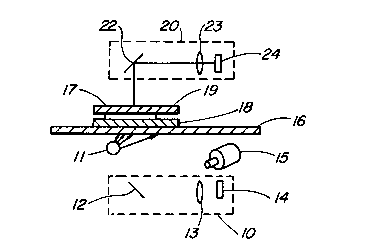
Figure 1 shows an optical reading apparatus
according to the invention. In the same way as the
apparatus of Figure 10, the apparatus of Figure 1
2~ comprises a transparent glass table 16 on which an
~riginal 17 is placed, a light source 11 disposed below
the glass table 16, a pulse motor 15 for movin~ the
glass table 16, and an optical reading unit 10 which
lncludes a mirror 12, a lens 13 and a line CCD
sensor 14 and is dis~osed beneath the glass table 16.
The apparatus of ~igure 1 further comprises another
optical reading unit 20 which includes a mirror 22, a
lens 23 and a llne CCD sensor 24, and is detachably
2~ 370
S5394
-- 6 --
supported above and in the vicinity of the glass
table 16 by a suitable supportin~ member tnot shown).
A diffusion plate 18 for scattering light beams from
the light source 11 ls sandwiched between the glass
table 16 and the original 17, and a transparent glass
depressor plate 19 is disposed on the original 17 for
holding the original a~ainst the glass table 16. The
pulse motor 15 moves the glass table 16 on which the
original 17 is placed, according to instructions from a
control circ~it described later.
When the original 17 is a transparent one,
light besms emitted from the light source 11 is made
uniform by the diffusion plate 18 and pass through the
transparent original 17 and glass depressor plate 19,
and the light path is bent by the mirror 22, after
whlch the light beams are converged by the lens 23 and
arrive at the line CCD sensor 24.
Figure 2 illustrates the line CCD sensors 14
and 24. These line CCD sensors 14 and 24 comprise a
line sensor unit 25 consisting of CCDs (Charge Coupled
Devices) S1 - SN, a transfer gate 26, an N-bit shift
register set 27 consisting of analog shift registers
SRl - SRN, and an output buffer 28. Electric charges
generated by the photoelectric conversion in the CCDs
Sl - SN are respectively transferred to the analog
shift registers SRl - SRN by a transfer pulse 0T
applied to the transfer gate 26, and then se~uentially
shifted to the output buffer 28 by shift clocks 01 and
~2 following the transfer pulse ~T~ In the ~utput
buffer 28, the charges are converted to a voltage
signal V0. An electric charge which has been shifted
2~103~0
S5394
. - 7 -
into the output buffsr 28 is reset by a reset pulse ~R
every tlme whenever another electric charge is newly
shifted into the output buffer 28. N~mely, a traln of
the signals ~0 is a voltage signal train, the level of
which corresponds to the amounts of the electric
charges generatsd in the CCDs Sl - SN d~ring the
previous scanning. The relationship between ~he
pul8es 0T~ 01~ ~2 and ~R and the voltage signal VO is
shown in Flgure 3. In Figure 3, vo i8 a voltage output
~h~ch is obtained by sample-holding the voltage
signals V0 in accordance wlth a sample-hold signal /SH,
and TCLAMp is a clamplng signal which ~s described
later .
1~ Flrst, the arrangemsnt of the embodiment will
be briefly described with reference to Figure 4. The
line CCD sensor 14 of the optical reading unit 10
re~eives the pulses ~T~ 2 and ~R from a control
clrcuit 38 to supply a voltage signal VOl to a sample-
hold clrcuit 30. The sample-hold circuit 30 samples
and holds the voltage signal V01 to genera~e an output
signal vol which is then supplied to an amplifier 31.
The amplifier 31 magnifies the level of the output
signal vol to generate an ~nalog signal VI~E01 which is
sent to a relay circuit 34. Similarly, the line CCD
sensor 24 o~ the optical reading unit 20 receives the
pulses ~T~ 01~ 02 and 0R from a control circuit 38 to
supply a volta~s signal V02 to a sample-hold
circuit 40. The sample-hold circuit 40 samples and
holds the volta~e signal V02 to generate an output
signal vo2 which is then supplied to an amplifier 41.
The amplifier 41 magnifies the level of the output
slgnal vo2 to genera~e an analog signal VI~02 which i~
201037(~
S5394
- 8 -
sent through a cab~e (not shown) to a connector 32.
Then, the analo~ signal VIDE02 is input to an
attenuator 33. The output VIDE02' of the attenuator 33
is sent to the relay clrcuit 34. The relay circuit 34
to which the analog signals VIDE01 and VIDEo2' are
lnput selects either of the two slgnals in accordance
with a signal TGATE supplied from the control
circult 38, to be supplled as a signal V~E0 to a
clamping circuit 35.
The clamping circuit 35 shifts the voltage
level of the slgnal VID~ withln the lnput range of an
AD converter 36. The AD converter 36 converts the
level-shlfted signal lnto dlg~tal data at the r~sing
edge o~ the sample-hold slgnal /SH. The AD
converter 36 ls an 8-bit converter, and the 8-bit
outputs D7, D6, ..., D0 are sent to a data p~ocessing
circuit 37. A lamp control circuit 39 lights the light
source 11 when a si~nal TLoN supplled from the control
circuit 38 is HIGH.
When a pulse motor drive circuit 42 receives
a pulse slgnal TpM once when a slgnal FO~WARD is HIGH,
the pulse motor 15 rotates ona step clockwise to move
the glass table 16 (Flgurs 1) forward 1/600 of an inch.
When the puls~ 8ignal TPM is received twice, the
table 16 is moved forward l/300 of an inch. ~he CCD
sensor 24 of the optical reading unit 20 comprises
2,550 CCDs (i.e., N ~ 2,550~, which is the number
required to read an 8.5 inch wide sheet at 300 dpi
(8.5 x 300). In contrast, the CCD sensor ~ of the
optical reading unit 10 comprlses 2,550 CCD sensors so
2~103 ~ 0
S5394
_ g _
that a sheet of a 4.25 lnch width can be read at a
resolution of 600 dpi.
Flgure 5 shows the clrcuit configuratlon of
the embodiment. In Flgure 5, ASW denotes an analog
switch, VOF 2 voltage follower, OP en operational
ampl~fler, R~Y a rel~y, snd A~C an AD converter.
With reference to Flgure 5, the arrangemen~
of the em~odlment wlll be described in more detail.
The sa~ple-hold circuit 30 comprises sn analog
switch ASWl, a capacitor Cl and a voltage
follower VOFl. The value of the t~m~ con~tant
(C3 x Rl) of the amplifier 31 is sufficlently larger
than the period T of the transfer ~ulse ~T. The
combinatlon of a capacitor C3 and a resistor Rl shifts
the level of the output slgnal vol down from
approximately 7 V to near 0 V as shown in Flgure 6, and
then the output signal vol undergoes a 3.6-fold
inverting amplificatlon in the operational
amplifier Pl ~i.e., R5/R3 - 3.6) to become the analog
slgnal VIDEOl.
The relay circuit 34 switches as follows:
5
when TGATE is LOW, VIDEO - VIDEOl,
hen TGATE i8 K~GH, VIDEO ~ VIDEO2~
That ~s, when the optical readlng unlt 20 for reading
transparent orlginals ~s attached, the signal TGATE
from the control clrcult 38 i8 set HIGH.
S5394
- ~0 -
In the clamping clrcui~ 35, an analog
switch ASW3 receives the signal TCLAMp from the control
circuit 38, and the level of the signal VIDE0
(approximately -1 V to +0.8 V) is shifted to be output
as a signal VIN whlch i8 greater than 0 V. The
sisnal VIN (from 0 V to +1.8 V~ $s input to the AD
converter 36. The AD converter 36 converts the input
signal VIN into digltal data while changing the its
level to 256 gradatlons from 0 V to 2 V, which is
performed at the rlse of the signal /SK.
In the ~ollowlng, the operatlon of the
embodiment when the optical reading unit 20 is attached
to read a transparent orlginal will be described. When
a transparent original is rea~, the voltage ou~put
signal V02 of the line CCD ~ensor 24 is sampled and
held in the sample-hold circuit ~0 to be ou~put as the
output signal vo2. Then, as shown in Flgure 7, the
output signal v~2 i8 shlfted down from approximately
7 V to ne~r 0 V and then undergoes invertlng
amplification in the operationsl amplifier OP2 to
become the signal VI~E02. The gain in this
ampliication i8 set at 7.2-fold, which is twice that
in the reflectlon readin~. The relationship between
the resistors R6 and R4 in the amplifier 41 is
R6/R4 ~ 7.2.
The reason for this is be~ause the slgnal
cable from the optlcal reading unit 20 is relatively
long as compared with thAt from the optical readin~
unit 10, making the signal VIDE02 suscept~ble to noise,
so its output level i8 made greater.
20103 ~0
SS394
- 11 -
Ths output slgnsl VIDE02 from the
ampllfler 41 ls supplied to the attenuator 33 which
comprises resistors R7 and R8. The reslstances of the
two reslstors R7 and R8 are equal to each other so that
the output signal YIDE02' of the attenuator 33 is
attenua~ed to one-hal the input slgnal VIDE02.
The signal VIDE02' i8 sent to the clamping
clrcuit 35 as the slgnal VIDE0 via the re}a~
circult 34. In the clamping circult 35, the ana~og
switch ASW3 receives the signal TCLAMp ~rom the control
circui~ 38, ~nd the leYel of the signal YIDE~
(approximately -1 V to ~0.8 V) is shifted to be output
as a signal VIN whlch ls greater than 0 V. The
lS signal VIN (from 0 V to +1.8 V) is input to the AD
converter 36. The AD converter 36 converts the input
signal VIN into dlgltal data while changing the its
level to ~56 gradatlons from 0 V to 2 V, which is
per~ormed et the rislng edg~ of the signal /SH.
Figu~e 8 shows the relationship between the
pulse s$gnal TpM and the transfer pulse 0T during the
reading of a reflectlve origlnal, which is performed at
a resolutlon of 300 dpi. Flgure 9 shows the
relationship between the pulse si~nal TpM and the
transfer pulse ~T durlng ths reading of a transparent
orlginal, which i8 performed at a resolution of ~00
dpi. By replaclng the optical reading unit 20 with
another optical readlng unit wlth another degree of
reading resolut~on such as 300 dpi or 1200 dpi, the
readlng of a transparent original can be performed at
any desired resolution.
2010370
S5394
- 12 -
When the electrlcal wlring from the optical
reading unlt (the optical reading unit 20) for a
transparent original i8 long to a degree that the image
lnformation signal from the reading unit i8 susceptible
to noise, a means (the amplifler 41) for amplify$ng ~he
signal is provlded in the above-descr$bed embodiment,
so that the level of the sisnal from the readlng unit
for a transparent origlnal is lar~er than that o~ the
signal from the reading unit (the optical reading
unit 1~ for a reflective original. Moreover, the
above-descrlbed embodlment is provided with a means
(the atten~ator 33) for attenuating the image
informatlon signal from the opticzl readlng unit for a
transparent orlginal which slgnal has bsen amplified,
thereby matching the output level with that of the
image information slgnal from the readlng unit for a
reflectiYe original, ~or the purpose of a further
signal processing. Conseguently, the optical reading
apparatus afore-descrlbed can be compact, manufactured
at an inexpensive cost and is capable of accurately
reading transparent orlginals with good resolution.
When the wlring from the optical reading unit
for a transparent original is not 80 long or the
2~ problem of noise is not 80 serious, however, the
amplifying means is not necessary, or alternatively the
degree of amplification can be decreased.
The gain or degree of amplification of the
amplifier 41 may be egual to that of the amplifier 31.
In this case, the attenuator 33 is not provided, and
the signal VIDE0 2 is directly input to the relay
circult 34.
2010370
S5394
According to the invention, both transparent
and reflectlve originals can be read with one
lnexpsnslve and compact optlcal reading apparatus.
Fu~thermore, t~ansparent originals can be read at a
deslred resolutlon by replacing the optional optical
unit wlth one wlth a dlfferent readln~ resolution.
It ls understood that varlous other modifica-
tions will be apparent to and can be readily made by
those skil1ed in the axt wlthout departing from the
scope and spirlt of this invention. Accordingly, it is
not intended that the scope of the claims appended
hereto be limited to the descrlptlon as set ~orth
hereln, but rather that the claims be construed as
encompassing all the features of patentable novelty
that reside ln the present lnvention, lncluding all
features that would be treated as equivalents thereof
by ~hose skll~ed ln the art t~ which thi~ invention
pertains.