Note: Descriptions are shown in the official language in which they were submitted.
- -1- RCA 85,41 6
VIDEO SWITCH ARRANGEMENT 20~0680
Field of the Inv~tion
This invention relates to the field of video switching
circuitry for a television receiver.
Background of the Inventi~n
The term television receiver as used herein includes
television receivers have a display device (commonly referred to as
television sets), and television receivers without a display dovice,
such as vidaocassette recorders (VCR's) and videodisc players.
Many modern television receivers include signal
switching circuitry for selecting a video signal and an audio signal
from a number of signal sources which may be connected to the
receiver. The selected signals are processed and ultimately
reproduced on a display screen, and at a speaker, respectively.
Signal switches in television receivers need to be of high quality
so as to not introduce distortion into the signals being passed
through thcm. More importantly, these switches should present a
high impedance to signals at their inputs when the switches are in
the ~off~ (non-conducting) state. Due to the highly competitive
nature of the consumer electronics businsss, these switches also :
must be inexpensive, especially for use in the "low and~ (less
expensive) television receivers. The characteristics of high
quality and high ~off state" impedance usually cause television
signal switches to be fairly high cost items. For example, the
TOSHIBA TA738P, a hi3h quality switch often used in top-of-the-
line television receivers, is approximately 5 times the price of the
switch circuitry of the subject invention to be described below.
In contrast to the process of selecting a particular
signal by means of a switch, it is well known to combine analo g
signals by means of an analog inclusive-OR circuit, commonly
known as a non-additive mixer (NAM) circuit. A representative
patent disclosing a NAM circuit
is U.S. patent 4,583,121 (Yost), issued 15 April 1986. Conventional
NAM circuits are not particularly well suited for use as switching
- 2 - RCA 85,416
2010680
circuits, because NAM circuits do not provide a selected signal, but
rather they provide a combined analog output signal which is equal
in amplitude to the amplitude of the greater of the signals at the
NAM circuit inputs.
It is herein recognized that a non-additive mixer (NAM)
circuit may be used as a switch by forward biasing one input of the
NAM circuit and reverse-biasing the other input or inputs. This is
accomplished by applying first and second signals, and first and
second bias levels of different magnitudes to respective inputs of
a level-gated^analog-OR circuit comprising a non-additive mixer
(NAM) circuit. The input receiving the greater bias level is enabled
thereby to convey its respective signal to the output of the NAM
circuit, and the input receiving the lesser bias level is prevented
from conveying its respective signal to the output of the NAM
circuit.
In another embodiment of the invention, a much simpler
(and therefore much less expansive) CMOS switching integrated -~
circuit (i.e., simpler than the TOSHIBA television signal switch
described above) is utilized to provide a selected signal and bias
voltage to one input of a level-gated-analog-OR circuit comprising
a NAM arrangement, while the other input is substantially
maintained at a low level.
The term ~level-gated-analog-OR circuit", as used
herein, refers ~o a circuit having multiple inputs for receiving
respective signals, one signal of which occupies a higher bias level
than the others. An output signal is developed in response to the
input signal having the higher bias level, and not in response to the
other input signals at the lower bias level.
Brief Description of the Drawin~
FIGURE 1 illustrates, partly in block diagram form and
partly in schematic form, an embodiment of the invention
comprising a switch arrangement disposed in saries with NAM
ci rcu itry.
3 P~CA 85.416
20~0680
FIGURE 1a illustrates a waveform suitable as an input
signal for the arrangement of FIGURE 1.
FIGURE 2 illustrates, in schematic form, an analog
signal and bias source suitable for use in the arrangement of
FIGURE 1.
FIGURE 3 illustrates, partly in block diagram form and
partly in schematic diagram form, another embodiment of the
invention .
FIGURES 3a and 3b illustrate waveforms useful in
understanding the embodiment of FIGURE 3.
Detail~j~Qtion of the Emb~
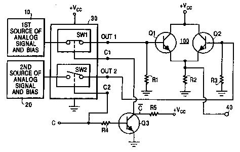
Referring to FIGURE 1, a non-additive mixer (NAM)
circuit 100 comprises two transistors Q1 and Q2 having their
respective collector electrodes coupled together and to a source of
supply voltage VCC, and having respective emittar electrodes
connected together and to one end of a single emitter resistor R2,
the other end of which is returned to ground. A multiple switch
unit 30 is disposed between signal and bias sources 10 and 20, and
respective base electrodes of transistors Q1 and Q2. Switch unit
30 may be a CD 4016B CMOS quad-switch device manufactured by
Harris Semiconductor Corporation, Somerville, New Jersey. A CD
4016B includes, in a single integrated circuit, the electronic
equivalent of four single-pole single-throw switches, only two
(i.e., SW1 and SW2) of which are shown for clarity. Each of these
switches has an individual respective control terminal C1 and C2
associated with it. Complementary control signals C and C?- for
controlling switches SW1 and SW2 of switch unit 30 are produced
by an inverter circuit comprising a transistor Q3 and resistors R4
and R5. Binary control signahC~ is applied to control input C2 for
controlling switch SW2, and complementary
control signal C?- is applied to control input C1 of switch SW1, so
that when switch SW1 is closed, switch SW2 is open.
-4- RCA 85,416
201068
In operation, signal and bias sources 10 and 20 produce
signals biased as shown in FIGURE 1a, and apply them to resp~ctive
inputs of switch unit 30. FIGURE la illustrates an analog signal
impressed upon a DC leval (V BIAS) such that the lowest ne~ative
excursion of the analo~ signal is at a positive potential of at least
lVBE with respect to a zero volt reference point. The analog
waveform is illustrated as a sine wave for simplicity, but may be,
for example, an audio or video signal. If binary control signal C is
at low level, then cornplementary control signal C? is at a high
lavel, causing SW1 to be elosed and SW2 to be open, as shown in
FIGURE 1. Accordingly, signals from signal and bias source 10 are
coupled to the base of transistor Q1, causing Q1 to function as an
emitter follower and to reproduce this signal at output 40.
Transistor Q2 has no si~nal driving its base because switch SW2 is
open, causing the base of transistor Q2 to be held at a ground
potential by resistor R3. Therefore, transistor a2 is reverse
biased by the signal and bias present on its eminer eleetrode and
presents a high impedanee to si~nals which may be present on its
base electrode. Speeifically, Q1 produees an analog signal across
emitter resistor R2 whieh is a reproduetion of the signal at the
base of Q1 but impressed upon a DC level whieh is 1VBE
(approximately 0.7V) lower than the DC level produeed by signal
and bias souree 10. Transistor Q2 is cut off from conduction due to
a rever~e bias eondition resulting from a zero volt level at its base
eleetrode and a DC level of VBIAs -1VBE at its emitter. That is,
the bias level of the aetive signal further euts off conduction in
the non-aetive transistor assoeiated with the non-selected signal.
By use of the arrangement of FIGURE 1, one of tNo signals is
provided at a single low impedanee point 40 (i.a., the emitter of
emitter follower transistor a1 or Q2).
Under the eonditions described above, transistor Q2 is
not eondueting, and its high impedance state is in caseade (in
series) with the high impedanee of open switeh SW2, thus fur~her
reducing any si~nal whieh may have leaked through open switch
SW2. Leakage of signal aeross the open switeh eontacts
~r
- - 5 - RCA 85,416
2010680
(sometimes called crosstalk) of the individual switches of a
CD4016B is typically approximately -46 db. By adding transistor
array 100 (i.e., the NAM circuit) as shown in FIGURE 1, the
crosstalk is further reduced by approximately an additional 20db,
which is of high enough quality to permit the use of this switching
arrangement in a top-of-the-line television receiver.
In FIGURE 1, transistor switch arrangement 100 serves
at least three purposes. First, it directs the output signals of
signal and bias units 10 and 20 into a single output line at point 40.
Second, it provides impedance transformation from the relatively
high switch impedance of switch unit 30 to a low impedance at
point 40. This reduces tendency to ~pick-up~ stray interfering
signals from other circuitry (e.g., horizontal rate pulses from the
horizontal deflection circuitry). Third, it provides additional
isolation to further reduce any leakage of signal which may occur
through open contacts of switch unit 30.
Referring to FIGURE 2, a circuit is shown which is
suitable for use as signal bias sources 10 and 20. An external
source of signal (not shown) is coupled to input terminal (or jack)
J1, which is of the typ~ which "shorts" the input line to ground (via
terminals 2 and 3) when a connector is not plugged in. Resistor
201 is a terminating resistor and, as such, typically has a value of,
for example, 75 ohms. Resistor 203 and diodes D201 and D203
form an input protection network for limiting electrostatic
discharge (ESD) or high amplitude signals which may be applied.
Likewise, a spark gap SG1 is provided for protection against
electrostatic discharge. The input analog signal is coupled via
coupling capacitor C201 to an amplifier stage 200 which inverts
the signal, amplifies it
and clamps it to a predetermined level. Amplifier 200 comprises a
transistor Q201 base bias resistors R205 and R207, an emitter
resistor R212 coupled to +V, a resistor R208 coupled to ground, and
a collector resistor R210. Resistor R208 shunts current around
Q201 and R210 and thereby affects the DC signal level at the
output terminal 210 without affecting the gain of amplifier 200.
In operation, amplifier 200 inverts the signal applied to its base,
, . . . .
. - - . . .
::
:: .
-6- RCA 85,416
~ 01(~681)
and clamps negative axcursions of the input signal to the positive
supply potential. Thus, the input signal is amplified and is
impressed upon a bias value, as required by the switch circuitry of
FIGURE 1.
In FIGURE 3, elements bearing the same reference
numbers as those in FIGURE 1 serw the same function, and
therefore need not be described again.
Referring to FIGURE 3, the base alectrode of transistor
Q1 is coupled to receive an analog signal produced by a first analog
signal and bias unit 10, which may include, for example, a comb
filter 12, and a bias circuit 14. Transistor Q1 may be included
within analog signal and bias unit 10 which may be, for example, a
comb filter unit such as the CF2601K comb filter manufactured by
TDK Corporation. The base electrode of transistor Q2 is coupled to
a bias network comprising resistor R3 and resistor R4, and is AC
coupled via capacitor C301 to receive an analo~ signal produced by
a second analog si~nal and bias unit 20 which may be, for example,
a source of video or chrominance signal, such as, an SVIDEO video
or chroma signal input terminal.
Operation of the circuitry of FIGURE 3 will be explained
with rehrence to the waveforms of FIGURE 3a and 3b. FIGURE 3a
shows two input waveforms, A and B, which for purposes of
explanation only, are shown as sine waves of opposite phase. In
actual practice, these signals may be television audio or video
si~nals havins li~tle or no phase relationship to one another. The
si~nal of waveform A is biased at a DC level of approximately 5
volts and is applicd to the base electrode of transistor Q1 of
FIGURE 3.
The si~nal of waveform B is biased at approximately 2 volts DC and
is applied to the base of transistor Q2. Transistor Q1 is forward-
biased and reproduces its signal -1VBE drop across emitter
resistor R2, as shown in FIGURE 3a as output waveform C.
Transistor a2 is reversed-biased because waveform C is, at all
points, more positive than is waveform B, which is applied to the
base of a2.
... - ,- ... ., ,, . . ~ , ,. . . ~
- 7 - RXCA 85 ,416
,
Referring to FIGURE 3b, the signal of waveform A,
applied to the base of transistor Q1, remains biased at a fixed level
of approximately 5 volts DC. The signal of waveform B, however, is
biased at approximately 8 volts DC, and is applied to the base of
transistor Q2. This causes transistor Q2 to conduct and develop a
signal of the type shown in waveform C of FIGURE 3b, across
emitter resistor R2. The output signal of waveform C is bias~d at
approximately 7.3 volts DC, and is thus at a significantly greater
level than the signal applied to the base of transistor Q1, causing
transistor Q1 to be reverse-biased.
Note that in the examples of FIGURE 3a and 3b,
waveform A (the signal applied to the base of Q1) was fixed at
approximately 5 volts DC bias, while the signal of waveform B is
switched between 2 and 8 volts DC bias. Referring to FiGURE 3, the
bias for transistor Q2 is set by resistors R3 and R4, but is
controlled by a switching transistor Q3 which receives a control
signal via resistor R305 from terminal 310. This control signal is
provided by a controller (not shown) in order to select signals from
source 10 or source 20. A high level signal at terminal 310
initiates conduction of transistor Q303 through resistor R303,
causing the base bias of transistor Q2 to be altered to
approximately 2 volts DC. A low level signal at terminal 310 turns
transistor Q303 off, causing the base bias of transistor Q2 to be at
approximately 8 volts DC.
Although transistor switching arrangement 100 was
shown as including only two transistcrs, it is herein recognized
that additional transistors may be connected in the same fashion.
Accordingly, the scope of the claims is not intended to be limited
to a two transistor arrangement.
Additionaliy, the scope of the claims is not intended to
be limited to the use of bipolar transistors because it is
recognized that FET devices are also suitable for use in practicing
the invention.
., - ~ , . .