Note: Descriptions are shown in the official language in which they were submitted.
Z01079'~
C-4110
G-2397
METHOD AND APPARATUS FOR INDUCTIVE LOAD
CONTRO~ WITH CURRENT SIMULATIO
FIELD OF THE INVENTION
This invention relates to method and apparatus
for controlling the current to an inducti~ve load and
particularly to such method and apparatu6 for
simulating the load current for feedback control
purposes.
BACKGROUND OF THE INVENTION
When controlling current to a motorr a
solenoid or other induçtive load, it is frequently
, . . . ., ~ _
desired to control the current by rapidly switching the
current on and off so that the average current meets a
desired goal or command value. The current switching
is generally accomplished by one or more switches in
series with the load and the power supply. When the
current is switched on it increases at a rate limited
by the inductive reactance of the load. when the
current is switched off it slowly decays at a rate also
determined by the inductive reactance. During the
current decay period a path must be provided for the
current, known as induced or recirculation current.
A co~mon motor driver circuit is an H-bridge
which has two arms connected from opposite sides of the
motor to the power source and two more arms connected
from opposite sides of the motor to ground. Each arm
contains a switch such as a power MOSFET so that by
selective switch control the motor can be driven in
either direction by current flowing fro~ the power
source and through the motor to ground. It is
convenient to use this type of driver in conjunction
2010794
with a driver interface when using a microcomputer to
control the motor. As is well known, load current
feedback is often desirable for comparison to the
command value to achieve closed loop control. The
recirculation current as well as the applied current is
required to be represented by the feedback. In the
case of the ~-bridge configuration, the motor current
is difficult tô sense because it is bidirectional and a
sensor would yield negative voltages at times and much
circuit complexity would be required to accommodate it.
SU~MARY OF TH~ INVENTION
.
It is therefore an object of the invention to
provide a method and apparatus to provide a motor or
- other inductive load control using a simple current
feedback. It is a further object to provide such a
control method and apparatus with a zero current
calibration feature using the current feedback
technique.
The invention is carried out by the method of
controlling current in an inductive load to a command
value comprising the steps of: applying current in one
direction to the load, charging a capacitor to a
voltage simulating the applied current, terminating the
applied current whereby an induced current flows
through ths load after such termination, the induced
current decaying at a rate determined by the load,
discharging the capacitor at a rate similar to the
decay rate of the induced current whereby the capacitor
voltage simulates the load current for both the applied
current and the induced current, and controlling the
current to the load by comparing the simulated value to
the command value and applying and terminating current
to maintain the simulated value close to the command
ZO~(~79~
value.
The invention is further carried out by a
circuit for controlling the current to an inductive
load to a command value comprising: means for
generating a command value representing a desired load
current, a power source, switch means for coupling the
load across the power source whereby an applied current
flows in the load and through the switch means when the
switch means is closed and a recirculation current
flows in the load when the switch means is open, means
responsive to the applied current flowing through the
switch means for generati~g a simulation signal
representing the recirculation current as well as the
applied current, and means responsive to the command
value and to the simulation signal for actuating the
switch means to control the load current to the command
value.
~RIEF DESCRIPTION OF THE DRAWINGS
The above and other advantages of the
invention will become more apparent from the following
description taken in conjunction with the accompanying
drawings wherein like references refer to like parts
and wherein:
Figure 1 is a block diagram of a contcol
system for an inductive load according to the
invention;
Figure 2 is a schematic diagram of a specific
control system according to the invention;
2010794
Figure 3 is an alternate driver and motor
configuration for use in the system of Figure 2; and
Figure 4 is a set of current waveforms
occurring in the load of Figure 3 when under regulation
according to the invention.
DESCRIPTION OF_THE PREFERRED EMBODIMENT
The description is directed to the control of
a solenoid or a motor in an H-bridge configuration but
it will be recognized that it is relevant to the
control of current to any inductive load.
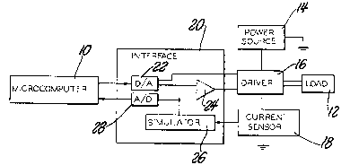
Figure 1 shows a microcomputer 10 as the
master control of current~supplied to a load 12 from a
power source 14. A driver 16 couples the power sourcs
to the load and a current sensor 18 completes the
return current path between driver 16 and the power
source 14. A motor driver interface 20 receives a
desired current command value in the form of digital
signals from the microcomputer 10 and a feedback signal
from the current sensor 18 and suitably switches the
driver 16 to apply an average current to the load 12
which corresponds to the command value. The interface
20 includes a D/A converter 22 which applies an analog
command value to a comparator 24. A simulator 26
receives a siqnal from the current sensor 18 and
provides a simulated load current to an input of the
comparator 24. The comparator ~hen produces an output
to the driver 16 to control switching to maintain the
load current near the value dictated by the command
signal. Other input~ from the interface to the driver
3~ may be used in the case of a motor to determinè motor
direction. An A/D converter 28 encodes the simulated
load current and supplies it to the microcomputer 10
which can use that information for calibration and
2010~9~
diagnostics.
The simulator circuit 26 is shown in Figure 2
and includes an amplifier 30 connected across the
current sensor 18 which comprises a resistor, a level
shift circuit 32, an amplifier 34 with a diod~ 36 at
its output and a feedback from the cathode of the diode
to the inverting input of the amplifier 34. The diode
36 is also coupled through a resistor 38 to a terminal
40. A filter circuit 41 co~prising a capacitor 42 and
a resistor 44 in parallel is connected between the
resistor 38 and ground. A pull-up resistor 46 is
connected from the terminal 40 to a 5 volt ~ource. The
values of resistors 44, 46 are chosen to develop a
voltage at terminal 40 equal to the level shift
voltage. This provides the controller with the
capability to more accurately control the current
through the load. The terminal 40 carries the
simulated load current signal and is connected to the
A/D converter 38 and to an input of the comparator 24.
The D/A converter 22 is connected through a level shift
circuit 48 to the other input of the comparator 24.
The purpose of the level shift circuits 32 and 48 is to
maintain the comparator at a discrete value above
ground voltage to enhance its operation. In this
example the load 12 is a solenoid and the driver 16 is
a single MOSFET with its gate coupled to the comparator
24 output; the load 12, driver 16 and current sensor 18
are serially connected between voltage V of the power
source and ground. A diode 50 is connected across the
load 12 and is poled to allow recirculation current.
Z01079'~
In operation, the comparator 24 compares the
level shifted command value to the simulated load
current signal at terminal 40. If the command value is
larger than the current by some comparator hysteresis
value, the output turns on the MOSFET to apply current
from the source through the load and through the sensor
18. A voltage proportional to the load current is
developed acros~ the sensor 18 and is applied to the
amplifier 30. The amplifier output is level shifted by
0.5 volt and is applied to the positive input of the
amplifier 34. The amplifier 34 and the series diode 36
along with the feedback line to the inverting input of
the amplifier 34 comprise a peak and hold circuit.
Thus the voltage applied to the terminal 40 tracks the
increasing load current but does not decrease when the
load current decreases. The increasing voltage is
stored on the capacitor 42 and is a measure of the load
current. When the voltage at terminal 40 reaches a
value above the command signal by a hysteresis amount
the comparator 24 output turns off the MOSFET 16 to
terminate the load current flowing through the sensor
18. A current continues to flow in the load 12 and
recirculates through the diode 50. The recirculation
current decays at a rate determined by the inductive
load 12 but this current is not directly measured.
Rather it is simulated by the capacitor 42 voltaqe
which discharges through the resistor 44 at a rate
determined by the time constant of capacitor 42 and
resistor 44. The time constant is selected to effect a
decay rate substantially the same as the decay rate of
the recirculation current. While the rest of the
circuit is suitably contained on an IC chip, the filter
circuit ~1 is preferably mounted externally so that the
2010794
time constant can be readily tailored to the load
characterlstics of a particular application. Thus the
voltage at the terminal 40 simulates the load current
at all times. When the simulated load current signal
decreases below the command level the comparator 24
again turns on the driver 16 to continue the current
regulation process.
The command signal may be varied by the
microcomputer 10 to dictate a corresponding variation
10 of ths load current. For example, if the load 12 is a
solenoid it will require a high current to pull in the
armature followed by a low holding current. Thus the
command value may call for 8 amps for a few msec and
then 3 amps for the remainder of the solenoid on period
and finally zero current to turn off the solenoid.
Another type of load is illustrated in Figure
3 which shows a motor 12' driven by an H-bridge 16'.
This load and driver is substituted for the load and
driver of Figure 2. The bridge has two upper arms 52
20 and 54 connected between the voltage V of a power
source and opposite sides of the motor and two lower
arms 56 and 58 connected between the opposite sides of
the motor and the current sensor 18. The arms 52 - 58
contain power MOSFETs 60 - 66 respectively for
individually switching the arms to apply current to the
motor 12'. The gates of the MOSFETs are controlled by
the interface 20 which has some additional logic to
selectively turn on certain MOSFETs. Each MOSFET has
an internal diode or body diode 68 poled to pa s
30 current in the direction opposite to the MOSFET
conduction. To drive the motor forward the MOSFETs 60
and 66 are turned on so that the motor current Im~ as
shown in Figure 4, is initially equal to the current
2(~10794
a
Ifl which flows through the MOSF~Ts from V to ground.
When the current exceeds the command value the MOSFET
66 is turned off but the MOSFET 60 remains on. Then
the recirculation current IreC flows through the motor,
the diode 68 of MOSFET 62 and the MOSFET 60. This
current is simulated in the simulator circuit 26. As
shown in Figure 4 the MOSFET is switched at a rate to
control the rise and fall times of the load currents
and thus minimize radio frequency interference. When
the applied current Ifl is turned off the motor current
Im is the recirculation current Ire~. When the current
Im goes above or below the command value enough to
switch the comparator 24, the MOSFET 66 is switched on
or off to regulate the motor current. As is well
known, reverse motor operation requires the MOSFETs 62
and 64 to be switched for applying Im in the opposite
direction. The current regulation proceeds in the same
way as for forward operation since the sensed load
current always flows in the same direction through the
sensor 18.
When the D/A commands a zero current the lower
MOSFETs 64 and 66 are turned off while the appropriate
upper MOSF~T 60 or 62 remains on to permit decay of the
recirculation current. Then no load current flows
through the sensor 18. After enough time has elapsed
for the si~ulated current signal to decay to
essentially zero, the terminal 40 voltag~ is sampled by
the ~icrocomputer via the A/D converter 28 to determine
the zero current reading. This value can then be added
to or subtracted from the simulated current signal when
current is flowing resulting in a more accurate current
value. This ~calibratingH can be done on a regular
basis, such as each software control loop while the
9 2010794
motor is turned off, to eliminate offset errors that
may occur over time and with temperature changes. This
calibration capability provides the control with
improved accuracy over other types of current control
circuits.
The foregoing description of a preferred
embodiment of the invention for the purpose of
illustrating the invention is not to be considered as
limiting or restricting the invention since many
modifications may be made by the exercise of skill in
the art without departing from the scope of the
invention.
3n