Note: Descriptions are shown in the official language in which they were submitted.
- 201 1 029
A FREOUENCY DETECTOR CIRCUIT
FIELD OF THE INVENTION
The present invention relates in general to digital
clock generating systems, and more particularly, to a
circuit for determining the validity of the frequency of
a clock signal.
BACKGROUND OF THE INVENTION
In modern digital telecommunication switching
systems voice samples are transferred within switching
systems, as well as, between remotely located switching
systems, as digital information. To preserve the integ-
rity of the digital information and thus insure high
quality voice communications, the telecommunication
network is synchronized.
Therefore, it is a requirement for a telephone
switching system to synchronize its local clock (slave)
to that of the network (reference). Synchronization of
the slave clock must be very precise and accurate since
other remotely located switching systems may be synchro-
nized to this switching system.
Synchronization between two clock signals is best
accomplished by the use of a Phase Locked Loop (PLL)
circuit. However, PLL circuits have several
disadvantages.
As the reference signal changes frequency the PLL
circuit follows these changes within certain limits.
Problems arise when the reference signal drifts outside
of these limits, or is completely lost, such as when a
cable is cut.
Because the amount that the PLL circuit frequency
will have drifted is proportional to the time it takes to
declare the reference frequency erroneous, a fast,
accurate method of frequency detection is necessary.
Prior to the present invention, frequency detection was
~'
- 201 1 02~
primarily accomplished by the use of mono-stable
vibrators.
The mono-stable vibrator would be designed to have a
period greater than the period of the signal to be moni-
tored, and the signal would constantly retrigger themono-stable vibrator before it would time-out. This type
of frequency detector can only detect if the frequency is
too low; a high frequency would continue to retrigger the
mono-stable vibrator within the time-out period and an
alarm condition would not be detected.
Additionally, mono-stable vibrators tend to drift as
a function of age and temperature which must be consid-
ered during their design. If accurate timing is needed,
the discrete resistors used by the mono-stable vibrator
are laser trimmed to provide an exact resistance, and
thus an accurate time-out period, a very expensive
process.
Accordingly, it is the objective of the present in-
vention to provide a frequency detector circuit which
rapidly detects an error condition when the frequency of
the signal being monitored is beyond a predetermined
limit.
SUMMARY OF THE INVENTION
In accomplishing the objective of the present inven-
tion, there is provided a novel circuit for determiningthe validity of the frequency of a reference clock
signal.
This circuitry for determining the validity of the
frequency of a reference clock signal includes a synchro-
nizer which receives the reference clock signal and syn-
chronizes it to a synchronous clock signal.
This circuitry also includes a pattern detector
which detects an error pattern from the synchronizer and
generates an error signal when the error pattern is
detected.
Finally, a latch is connected to the pattern detec-
tor which latches the error signal.
20 1 1 029
-
DESCRIPTION OF THE DRAWINGS
A better understanding of the invention may be had
from the consideration of the following detailed descrip-
tion taken in conjunction with the accompanying drawings
in which:
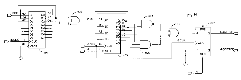
FIG. 1 is a schematic diagram of the frequency de-
tector circuit shown in FIG. 1.
FIG. 2a is a timing diagram for the circuit of FIG.
1, showing the state of selected signals for normal
operation.
FIG. 2b is a timing diagram for the circuit of FIG.
1, showing the state of selected signals when the refer-
ence frequency is completely lost.
FIG. 2c is a timing diagram for the circuit of FIG.
1, showing the state of selected signals when the refer-
ence frequency is doubled.
FIG. 2d is a timing diagram for the circuit of FIG.
1, showing the state of selected signals when the refer-
ence frequency is cut by one-half.
DESCRIPTION OF THE PREFERRED EMBODIMENT
Turning to FIG. 1, a general description of the pre-
sent invention will now be given.
The frequency detector circuit compares the signal
to be monitored (the reference signal REF) with a second
signal (SCLK), looking for a predetermined bit pattern.
If this pattern is found, then the input signal has
drifted beyond acceptable limits and an alarm is sig-
naled. The second signal must be an integer multiple of
the signal to be monitored, and in the present invention
it has a frequency of four times the monitored signal.
The frequency detector circuit of the present invention
allows an erroneous signal to be detected in a maximum of
four and one-half (1/2) clock cycles of the second signal
after the fault.
Looking at FIG. 1 in more detail, the signal to be
monitored REF is first delayed through three D-FFs in
401. Device 401 has a total of eight D-FFs in one
20 1 1 029
package all having a common clock signal and output
enable signal. However, for the present invention only
three D-FFs with a common clock signal are required. The
outputs of the second and third D-FFs in 401 are
connected to an EXCLUSIVE-OR gate 402. Under normal
conditions, the output of 402 (PH0) will be a clock
signal with a frequency of two times (2x) that of the
reference. The output of 402 is again delayed by three
D-FFs in 403. Device 403 has a total of four D-FFs in
one package all having a common clock signal and clear
signal also both output polarities of each D-FF are
provided. However, for the present invention only three
D-FFs with a common clock signal and both output
polarities of each D-FF are required.
NAND gates 404, 405, and 406 are arranged to detect
three consecutive logic highs or logic lows in the clock
stream of 402. If detected, an alarm signal is latched
by JK-FF 407. It must be understood that in the present
invention, SCLK has a frequency of four times (4x) that
of REF.
With renewed reference to FIG. 1, and with the aid
of FIGs. 2a, 2b, 2c, and 2d, a detailed description of
the operation of the frequency detector will be given.
The frequency detector circuit compares the signal
to be monitored (REF) with a second clock signal (SCLK).
The second clock signal counts the state transitions of
the REF signal, effectively monitoring the period of REF.
If the period of REF increases or decreases by more than
thirty three percent (%33), then the REF signal has
drifted beyond acceptable limits and an alarm is
signaled.
The signal to be monitored REF is first clocked by
the rising edge of SCLK into a series of three D-FFs in
401 of which the second and third outputs are connected
to the EXCLUSIVE-OR gate 402. It will be appreciated by
those skilled in the art that, the first and second D-FFs
of 401 form a double buffer, whereby any set-up or hold
time violations are not propagated through the frequency
detector. This removes any requirement on phase
,.
20 1 1 02q
relations between REF and SCLK. However, there still
remains a frequency relationship required by the present
invention. The relationship chosen by the present
invention is that the SCLK's frequency is four times (4x)
that of REF.
As is shown in FIG. 2a, under normal conditions, the
output of EXCLUSIVE-OR gate 402 (PHO) is a clock signal
with a frequency of two times (2x) that of the REF. The
output of EXCLUSIVE-OR gate 402 (PHO) is clocked by the
falling edge of SCLK into another series of three D-FFs
in 403. If the falling edge of SCLK clocks in three
consecutive logic lows, NAND gate 405 will output a logic
low. If the falling edge of SCLK clocks in three
consecutive logic highs, NAND gate 404 will output a
logic low. Should either NAND gate 404 or NAND gate 405
output a logic low signal, NAND gate 406 will output a
logic high signal and the next falling edge of SCLK will
clock an alarm signal out of JK-FF 407.
In FIG. 2b, REF is completely removed and the resul-
tant signals are traced. When the falling edge of SCLK
clocks in three consecutive logic lows into the three
D-FF of 403, NAND gates 405 and 406 detect an alarm con-
dition which is latched by JK-FF 407. FIG. 2b shows that
it takes four and one-half (1/2) cycles of SCLK to detect
the fault.
In FIG. 2c REF is suddenly doubled in frequency. In
this case, the falling edge of SCLK clocks in three con-
secutive logic highs into the three D-FF of 403, NAND
gates 404 and 406 detect an alarm condition which is
latched by JK-FF 407. FIG. 2c shows that it takes four
and one-half (1/2) cycles of SCLK to detect the fault.
In FIG. 2d REF is suddenly halved in frequency. In
this case, the falling edge of SCLK clocks in three con-
secutive logic lows into the three D-FF of 403, NAND
gates 405 and 406 detect an alarm condition which is
latched by JK-FF 407. FIG. 2d shows that it takes four
and one-half (1/2) cycles of SCLK to detect the fault.
Although the preferred embodiment of the invention
has been illustrated, and that form described, it will be
,~
20 1 1 02~
readily apparent to those skilled in the art that various
modifications may be made therein without departing from
the spirit of the invention or from the scope of the
appended claims.