Note: Descriptions are shown in the official language in which they were submitted.
2011~68
28151-12
SEMIC01~DllCTOR LASER DRIVING CIRCUIT
Background of the Invention
Field of the Inventlon
The present invention relates to a semiconductor laser
driving circuit and, more particularly, to a semiconductor laser
driving circuit comprising an output circuit composed of a
plurality of transistors connected in parallel and a current
source.
Brlef Description of the Drawings
Figure 1 is a circuit diagram of a prior art
semiconductor laser drivlng circuit;
Flgure 2 is a graph for showing the collector current
for optlmum transistor characteristics;
Figure 3 is a graph illustratlng a drivlng pulse current
for obtainlng a desired llght output;
Flgure 4 shows the collector current versus operatlng
frequency characteristics for a transistor;
Flgure 5 is a wave~orm dlagram lllustratlng the hlgh-
speed response characterlstlcs of the tran61stors and the
semlconductor la~er ln the drlvlng clrcults
Flgure 6 ls a schematlc clrcult dlagram lllustratlng the
prlnclple of a semlconductor laser drlvlng clrcuit accordlng to
the present lnventlon~ and
Flgure 7 illustrates an embodlment o~ the semlconductor
laser drlving circult accordlng to the present lnventlon;
Flgure 8 lllustrates another embodlment of the
semlconductor laser drlvlng circuit accordlng to the present
lnventlon, and
A ~
~ .. , . . -
.. .. ... . ~ ..
2011168
2 28151-12
Figure 9 illustrates a further embodiment of the
i semiconductor laser driving circuit according to the present
invention.
Description of the Related Art
Semiconductor lasers used in llgh~ output circuits for
optical communication during daytime require driving circuits
, which accommodate variations in values of components used and
variations in temperature.
Figure 1 illustrates an example of a prior art
semiconductor driving circuit. This circult comprises a parallel
circuit 2 having n (n~l) transistors Trll to Trln connected ln
parallel and a parallel circuit 20 having n transistors Tr21 to
Tr2n connected in parallel. Circuits 2 and 20 together constltute
a dlfferentlal pair forming a differential amplifier. A common
base lnput Vl of parallel circult 2 and a common base lnput V2 of
parallel clrcult 20 are supplled wlth pulse slgnals of opposlte
polarltles.
r~
,~
:.
., - :
. .
$
~ ~,
When the common base input V1 is on, transistors Tr11
to Tr1n are all turned on so that a semiconductor
laser 1 is driven by a current source 3 to emit a
desired light output pulse. The differential pair
portion shown by broken lines in Fig. 1 is usually
used in the form of an integrated circuit (refer to
Japanese Unexamined Patent Publications Nos. 57-10279
and 63-119281).
' With the circuit of Fig. 1, the number of
transistors constituting parallel circuit 2 is pre-
selected such that a (rated) collector current is
allowed to flow through each transistor, optimizing
the characteristics of each transistor, i.e., which
maximizes the current amplification factor hFE, like
the collector current Ic1 shown in Fig. 2 when an
allowable maximum current flowing through the
semiconductor laser 1 is divlded equally by
transistors Tr11 to Tr1n.
The current source 3 is designed so that its
current Io (= Ip) can be varied in order to produce a
driving pulse current Ip which generates a desired
light output Po to flow through the semiconductor
~ laser 1, as shown in Fig. 3, when the current Ip
¦ flowing through the semiconductor laser 1 is varied by
~ 25 variations in the elements used and by variations in
t
~ : '
2û~ ~16~s
tempera ture .
With such a semiconductor laser driving circuit,
however, the driving pulse current Ip may be small and
the driving pulse current Ip may have to be increased.
This depends upon variations in the semiconductor
laser 1 and variations in temperature. If the current
Io of current source 3 is varied accordingly, the
collector current f lowing through each of the
transistors will become, for example, Ic1 (where the
current amplification factor has a maximum value of
hFE1 ) or Ic2 (where the current amplification factor
is hFE2 less than hFE1). These different collector
currents Ic1 and Ic2 will result in different
operating frequency characteristics, as shown in Fig.
4.
As a result, the high-speed response
characteristics of each transistor, particularly the
waveform rising and falling characteristics for Ic2
shown by the broken line in Fig. 5, will be
significantly degraded compared with those for Ic1
shown by the solid line in Fig. 5. The light output
waveform of semiconductor laser 1 will be simllarly
degraded .
Summary of the Invention
It is accordingly an object of the present
. .
- . .:. .:. -
-:. . ':
2 0 ~ 8
28151~12
invention to provide a semiconductor laser driving circuit which
avoids the degradation of high-speed response characteristics of
each transistor in the driving circuit even if a driving pulse
current flowing through a semiconductor laser is varied.
According to a broad aspect of the invention there is
provided a semiconductor laser driving circuit for driving a
semiconductor laser comprising:
~ a current source capable of supplying a current to the
;: semlconductor laser;
a group of transistors, each having a respective maxlmum
current amplifylng rate, connected to said current source; and
means for selectively connectlng a number of translstors from
said group ln parallel with one another and to the semiconductor
laser such that a current characteristic of sald semiconductor
laser matches a sum of optimum currents for the number of
transistors thereby each transistor operating at a current
exhibiting its maximum current ampllfylng rate.
According to another broad aspect of the inventlon there
is provided a semiconductor laser drlving clrcuit for driving a
semlaonduator laser havlng a current characterlstlc comprislng,
a current source capable of supplying a current to the
semlconductor laser~
a group of translstors, each having a respective optlmum
current and coupled to said current source; and
means for selectively connectlng a number of translstors from
sald group ln parallel wlth one another such that the current
~c~aracterlstic of the semlconductor laser matches a sum of the
¦ ~ptimum currents for the number of transistors.
-:
2011~8
5a 28151-12
According to another broad aspect of the invention there
is provided a method of compensating a circuit for drlving a
semiconductor laser comprising the steps ofs
. (a) fabricating the circuit with a group of transistors;
: (b) determining an optimum current for one of the
. transistors;
(c) determining a maximum value of a driving pulse current
of the semiconductor laser;
(d) dividing the maximum value of the driving pulse current
in said step (c) by the optimum current ln sald step (b) to
determlne an lntegral number;
(e) operatively coupllng in parallel a number of translstors
from the group of translstors equal to the lntegral number after
fabrlcating the circuit wlth the group of transistors in said step
(a)-
. ~
-
.,~ ~' '
'' : ,
.' ' ' ' ' ' :::
201~:~6~
Detailed Description of the Preferred Embodiments
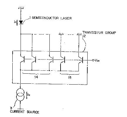
As shown in Fig. 6, which illustrates the
principle of the invention r the semiconductor laser
driving circuit comprises a current source 3 for
supplying a current to a semiconductor laser 1 and a
transistor group 12 in which a plurality of
transistors are connected in parallel. A
predetermined number of transistors 14, connected in
parallel and selected from the transistor group 12,
are connected between the semiconductor laser 1 and
the current source 3.
The number of transistors forming the transistor
group 12 is set such that, when an allowable maximum
current flowing through the semiconductor laser 1 is
1S equally dlvided by all the transistors of the
transistor group 12, a collector current flows through
each of the transistors which optimizes its
characterlstics (that ls, the current amplification
factor hFE has a maximum value).
~;~ 20 Also, the number of translstors 14 to be selected
from the transistor group 12 is set such that a
current Ip for generating a required light output Po
flows through the semlconductor laser 1 and the
optlmum collector current flows through each of the
transistors 14.
.
,' ' , ' ' "'
" ~ "'
, .
; `' ' " ' '~"'','` ` ' ' '' ' ,...... .
'
2 0 ~ 8
,.
-- 7
`~
It is also possible to supply the optimum
s; collector current to each of the transistors 15 as
~, well as to the selected transistors 14 in the
~- transistor group 12, from the current source 3.
By setting the number of transistors forming the
transistor group 12 and the number of transistors 14
connected to the semiconductor laser 1 as described
...:
, above, the present invention produces two main
advantages.
Firstly, the driving pulse current Ip flows
through the semiconductor laser 1, which causes the
, laser 1 to dellver the required light output Po (refer
to Fig. 3), and the same optimum collector current
always flows through each of a predetermined number of
transistors 14 connected to the semiconductor laser 1.
Therefore, the collector current of each transistor
has an optimum fixed value, such as Ic1, as shown in
Fig. 2, even if the driving pulse current Ip varies
from sample to sample o~ a given type of semiconductor
laser used. This prevents degradation of the hlgh-
speed response characterlstics (rising and falling
characteristics) of each of the transistors used.
Secondly, if the transistors 15 as well as the
selected transistors 14 in the transistor group 12 are
connected to the current source 3 so as to be supplied
:
~' ' ~ ' ~ .
; ~ .
.i. ~ ,
2 0 ~
-- 8
with the optimum collector current therefrom, stray
capacitance can be eliminated from the transistors 15
and a driving circuit comprising the transistor group
12 can be used as one of a differential pair. This
will allow the semiconductor laser to be driven with
faster response characteristics.
In each of the embodiments of Figs. 7 and 8, a
semiconductor laser driving circuit comprises a
differential pair composed of a transistor parallel
circuit 20 as in the prior driving circuit shown in
Fig. 1 and a transistor group 12 having the same
number of transistors as the transistor parallel
circuit 20. In these embodiments, the current Io of
the current source 3 is selected so as to accommodate
the maximum value of the driving pulse current Ip,
which is sub~ect to variation due to manufacturing
processes, of the semiconductor laser 1.
The number n of translstors constituting the
differential pair in the translstor group 12 i9
selected such that n ~ Io/Ico, where Ico is the
; optimum collector current for a transistor and Io is
the current supplied by current source 3. Thus, the
collector current Ico supplied to the semiconductor
laser 1 by one of the transistors is given by Io/n.
In the embodiment of Fig. 7, the optimum driving
: ' .
, ~- ' - .
-
... . . .
20~168
pulse current Ip (refer to Fig. 3 ) f or the
semiconductor laser 1 is 2Io/n. For this reason, two
transistors Tr11 and Trl2 are connected in parallel
between the semiconductor laser 1 and the current
source 3. The other transistors Tr13 through Tr1n
have their emitters connected to the current source 3
and their collectors connected to ground.
In the embodiment of Fig. 8, on the other hand,
the semiconductor laser 1 requires a driving pulse
current of n x Io/n. Thus, in this case, all the
transistors Trl1 through Tr1n are connected in
parallel between the semiconductor laser 1 and the
current source 3. In general, where the semiconductor
laser 1 requires m x Io/n (m 5 n) as its optimum
driving current Ip, m transistors are arbitrarily
selected from the transistor group 12 and connected
between the semiconductor laser 1 and the current
source 3.
The embodiments of Figs. 7 and 8 are distinct
from each other in the optimum driving pulse current
Ip for the semiconductor laser 1. However, in both
embodiments, the current flowing through each of the
transistors in the transistor group 12 has a constant
value of Io/n, independent of the magnitude of the
driving pulse current for the semiconductor laser.
2~1~168
- 10 -
,,
For this reason, even if the characteristics of
the semiconductor laser 1 vary from sample to sample,
the switchin~ current flowing through the transistor
`- group 12 always amount to Io, which is identical to
that of the transistor parallel circuit 20, thus
forming a differential pair with the transistor group.
Thus, the degradation in the high-speed response
characteristics of the driving circuit can be
minimized.
In the above embodiment, the driving circuit is
formed of a differential pair. However, a
differential pair conflguration may not be needed so
long as bipolar transistors are used. In addition,
~, the transistors 15 as well as the transistors 14
connected to the semiconductor laser 1 are connected
to ground. This is to allow the same current to flow
through each of the transistors in transistor group 12
and transistor parallel circuit 20, which form the
~:
~; differential pair, and to ellminate stray capacitances
and thereby achieve a high-speed response. Even where
the transistors 15 are not supplied with current,
degradation of waveforms i9 prevented.
Furthermore, if the transistors constituting
transistor group 12 have their emitters connected
together and their bases connected together, their
~;:
:
:
.
,...... ...
:.
::: . - -
, ~
. ~ ,
~- . .
2~L3 .~8
- 11 -
collector currents remain unchanged. Thus, it is not
necessarily required to directly connect all of the
transistors 15 to ground as shown in Fig. 7. For
example, suitable resistors may be connected between
S the transistors 15 and ground. Alternatively, another
semiconductor laser 11 may be connected between the
transistors 15 and ground as shown in Fig. 9. In this
case, if the semiconductor lasers 1 and 11 have
different characteristics, the number of transistors
to be connected to them will vary according to these
characteristics.
The transistors 14 may be connected to
semiconductor laser 1 by bonding with a conductive
material. Alternatively, the selection of transistors
may be made by means of a switch between the
transistor group 12 and the semiconductor laser 1.
In the above embodiments, npn bipolar transistors
are used. Of course, pnp bipolar transistors may be
used instead. In thls case, each pnp transistor has
its emitter electrode tone oi its main electrodes)
connected to the semiconductor laser 1 and its
collector (the other of its main electrodes) connected
to the current source 3. If the driving circuit is
arranged such that currents flow in the opposite
direction, the transistors are disposed accordingly.
.
-'~
:~ 20~
r
- 12 -
As described above, according to the present
s invention, by connecting a predetermined number of~ transistors selected from a group of transistors
i, .
connected ln parallel between a semiconductor laser
and a current source, a semiconductor laser driving
circuit can be arranged such that a current flows
through the semiconductor laser to deliver a reguired
` light output and an optimum collector current flows
through all of the predetermined transistors.
Accordingly, the collector current of all of the
transistors always has a constant optimum value
irrespective of the magnitude of the current necessary
for the semiconductor laser. Thus, optimum high-speed
response is always achieved.
If, in that case, transiettors other than those
~; connected to the semiconductor laser are equally
supplled with an equal optlmum collector current, the
drlving clrcult can be used ln the form of a
dlfferentlal palr, thus elimlnating stray
capacltances, Accordlngly, a semlconductor laser
drlvlng circult wlth faster response characterlstlcs
can be lmplemented.
;~
" .,` ~
.
, ~ ~ .
.~
1 ~`
.. -: : :, -
~,: ~,
. .