Note: Descriptions are shown in the official language in which they were submitted.
2011~L7~
Description
Integrated Optic Star Coupler
Technical Field
This invention relates to optical signal star
couplers, and more particularly to integrated optic
(IO) devices therefor.
Background Art
In fiber optic systems, such as fiber-optic
gyro (FOG) and coherent optical communication
systems, the system's accuracy requires a precise
knowledge of the optical signal phase. As an
example, the rotation rate in a FOG system based on
the Sagnac principle is determined by comparing the
optical phases of two optical signals, e.g. light
beams, propagating in opposite directions through an
interferometric loop. Similarly, in a coherent
communication system the information is encoded onto
an optical signal by temporally varying the light
beam's phase in the transmitter, and the encoded
information is decoded at the receiver by comparing
the phase of the transmitted light beam to the phase
- of a reference light beam.
To obtain optimum performance in these phase
sensitive systems it is critical that the optical
signal in the fiber is linearly polarized, and
confined to one of the orthogonal polarization
modes. The two orthogonal polarization modes (TM
and TE) are not degenerate, i.e. they have slightly
different phase velocities. If power is coupled
from one polarization mode to the other the optical
-- 1 -- ~
R-3233hs-ed ~
201 1 470
phase at the FOG detector (or the communication
system receiver) will be perturbed. This results in
drift errors for the FOG system and increased noise
and signal fading in the coherent optical communi-
s cation system. It is obvious, therefore, that phasesensitive optical systems must be fabricated using
optical components which are polarization
preserving.
One standard optical component required in
10 each system is a polarization preserving, N x M star
coupler. These N input / M output star couplers may
range from , and include, 1 x M splitters to N x 1
multiplexers. The star coupler accepts optical
signal power from N inputs, combines the N input
15 powers into a single guide, and then splits the
guide output into M equal parts.
The key parameters for the coupler are:
(i) the splitting uniformity, (ii) the insertion
loss (sum of the M output powers divided by the sum
20 of the N input powers), and (iii) the polarization
extinction (the output power in the desired
polarization mode divided by the output power in the
undesired polarization mode). The ideal coupler
would have a uniform splitting ratio, zero excess
25 insertion loss, and infinite polarization
extinction.
Some of the prior art polarization pre-
- serving star couplers are fiber optic devices, which
are fabricated either through the fusion elongation
method or the mechanical polishing method. In the
fusion elongation method 2 x 2 (N x N) star couplers
are made by thermally fusing two polarization pre-
serving optic fibers, and then elongating them in
the waveguide portion. The cores of the two fibers
. .
~, -
2011~7~
must be in close proximity when fused so that in
operation power transfer can occur between fibers
via evanescent coupling.
The polarization axes of the fused fibers must
also be perfectly aligned in parallel to preserve
polarization modes in this fused coupling region.
In the mechanical polishing method, the polished
surface of two optic fibers are joined using an
index matching liquid bond. Power transfer again
occurs through evanescent coupling, so that the
fibers must be in close proximity and must be
aligned.
Both fabrication methods produce devices which
have low excess insertion loss and relatively
uniform splitting. However, the polarization
extinction ratio is typically degraded due to
angular misalignment of the polarization axes of the
two fibers, unless the fiber geometry is designed to
physically establish the main polarization axis
easily, such as with the use of rectangular fibers.
For these reasons, fiber star coupler configurations
larger than 2 x 2 are impractical. One alternative
is to cascade a series of 2 x 2 couplers to achieve
the desired N x M result. Another alternative is to
use feedback looping and tapping.
The prior art IO star couplers are fabricated
by cascade arrangement of 1 x 2 splitters in tree
structures. The splitters may be Y-junctions or
directional couplers, and are fabricated on a
substrate material. The substrate materials include
glass and LiNbO3. For glass substrates the splitter
circuitry is deposited on the substrate surface
using an ion exchange method. In the case of LiNbO3
201 1470
substrates, the titanium diffusion method is used to
deposit the circuit configuration.
The prior art IO star couplers are
polarization maintaining to a degreei similar to the
5 polarization preserving characteristics of the optic
fiber couplers. They are not single polarization
devices, i.e. they do not have high polarization
extinction.
The object of the present invention is to
10 provide a single polarization IO star coupler.
In accordance with a particular embodiment
of the invention, there is provided a single
polarization integrated optic (IO) star coupler,
comprising:
substrate means, comprising a refractive
material having a major surface; and
star coupler array means, including one or
more 1 x 2 optical power splitter means disposed in
cascade on said major surface to provide an array
20 having N number of signal inputs and M number of
signal outputs arranged in an N x M star coupler
architecture;
as characterized by:
said star coupler array means being formed
25 in said major surface by a two step proton exchange
(TSPE) process comprising the steps of:
immersing said substrate, for a period of
from two to sixty minutes, in a benzoic acid bath at
a temperature of from 150C to 250C;
removing said substrate from said bath
following said step of immersing; and
annealing said substrate for a period of
from one to five hours at a temperature of from
300C to 400C.
: - 4 -
.,
~
201 1 470
According to the present invention a
single polarization IO star coupler comprises a
crystalline material substrate having a star coupler
waveguide array formed in a major surface thereof by
5 a two step proton exchange (TSPE) process. In
further accord with the present invention, the star
coupler waveguide array includes one or more 1 x 2
splitters disposed in cascade to provide an array
having N number of signal inputs and M number of
,10 S ignal outputs, which are arranged in an N x M tree
architecture. In still further accord with the
present invention, each 1 x 2 splitter comprises a
symmetrical Y-junction node. In still further
accord with the present invention, the star coupler
15 substrate material comprises, alternatively, LiNbO3
and LiTaO3. In still further accord with the
present invention, the substrate material may
-include, alternatively, an X-cut, Z-cut, and Y-cut
crystal orientation.
The N x M IO star coupler of the present
invention includes a waveguide array having a 1 x 2
splitter as a basic building block. One or more 1 x
2 splitters are arranged in selected geometric
patterns on the substrate surface to achieve any
25 desired N x M splitting or combining transfer
functions, as may be known to those skilled in the
art.
Preferably, the 1 x 2 splitter is a
symmetrical Y-junction node. The Y-junction and
- 30 connecting waveguide paths are fabricated on either
- LiNbO3 or LiTaO3 substrate material using a TSPE
process. This involves immersion of a patterned
array substrate in a concentrate benzoic acid bath,
followed by substrate annealing. This provides a
. ~ .
201 1470
-
star coupler having high polarization extinction to
provide an integrated optic (IO) star coupler having
a uniform splitting ratio and low loss
characteristics.
These and other objects, features and
advantages of the present invention will become more
apparent in light of the detailed description of a
best mode embodiment thereof, as illustrated in the
accompanying drawing.
Fig. 1 is a perspective illustration of a
basic Y-junction node 1 x 2 star coupler according
to the present invention;
Fig. 2 is a schematic illustration of a
2 x 2 star coupler using a plurality of the Y-
15 junction nodes illustrated in Fig. l;
Fig. 3 is a schematic illustration of a
1 x 8 star coupler using a plurality of the Y-
junction nodes illustrated in Fig. l; and
Fig. 4 is a schematic illustration of a
20 4 x 4 star coupler using a plurality of the Y-
junction nodes illustrated in Fig. 1.
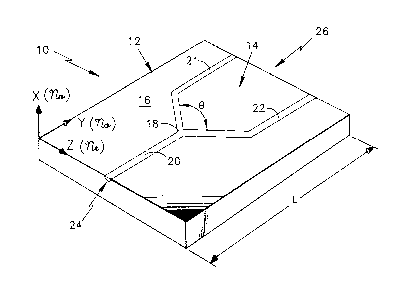
Fig. 1 is a perspective illustration of a
1 x 2 star coupler 10 according to the present
invention. The star coupler includes a crystalline
25 material substrate 12, which provides a refractive
medium for a waveguide circuit array 14 disposed on
a substrate major surface 16. The substrate
material may be either LiNbO3 or LiTaO3. Preferably
the substrate has an X-cut crystal orientation, but
30 Z-cut and Y-cut crystal may also be used. The
extraordinary index of refraction (ne) for the X-cut
crystal lies along the Z axis.
201 1 470
.
The array 14 includes a Y-junction node 18
and three single mode waveguides 20-22. For
purposes of description only, the waveguide 20 shall
be referred to as the "single waveguide interface"
5 24 of the star coupler, i.e. the single signal input
side, and the waveguides 21, 22 are termed the
"first" and "second" waveguides of the star
coupler's "dual waveguide interface" 26. The
substrate has an overall length (L) between the
10 interfaces.
If the node is symmetrical and the
splitting angle e 28 is not too large, i.e. e is
from 1 to 2 degrees, the optical power in guide 20
is split equally (within device tolerances) into the
15 guides 21, 22. For these same splitting angle
conditions, the optical power of signals presented
to the guides 21, 22 is combined in the guide 20 to
a power level equal the sum of the individual power
levels at the guides 21, 22, less the loss occurring
20 in the device, less any additional loss due to phase
mismatch or incoherence of the optical signals
arriving at the Y-junction.
In the best mode embodiment the Y-junction
node is symmetrical; having three equal legs and a
25 splitting angle e in the range of 1 to 2 degrees.
If the optical signals presented to the guides 21,
22 are not in phase there is a destructive com-
bination of the two signals at the Y node, which may
excite other modes in the waveguide 2~, causing some
30 portion of the light intensities of the two signals
to leak into the substrate 12. Furthermore, if the
two signals are not coherent, each will suffer a 3
dB loss upon going through the Y-junction. There-
201 1 470
fore, the ideal combiner function of the device is
limited to a combination of equally phased coherent
signals. This of course is well known to those skilled
in the art of integrated optic (IO) devices.
The circuit array is fabricated on the substrate
using the two-step proton exchange (TSPE) process
disclosed and claimed in a commonly owned, copending
patent application of the same assignee, filed on even
date herewith by Suchoski et al., entitled Low-Loss
Proton Exchanqed Wavequides for Active Inteqrated Optic
Devices, U.S. Patent No. 4,984,861 issued January 15,
1991 .
Fabrication of the star coupler begins with
deposition of a masking layer of material, such as
aluminum (Al), chromium (Cr), titanium (Ti), or silicon
dioxide (SiO2), on the surface 16. A photoresist film
is then deposited on the surface. The resist film is
patterned in the desired circuit array geometry. The
patterned film is then exposed to ultraviolet light and
developed to duplicate the pattern on the masking
layer. The surface is then etched to expose the
circuit geometry, i.e., the waveguide channels, on the
surface. The channel widths vary with the intended
guided signal wavelength, but range from 3 to 10
microns. The masking pattern limits the proton
exchange to the channel etched areas.
The substrate is then immersed in a
concentrated benzoic acid bath for two to sixty
minutes. The acid bath is at a temperature of from
150C to 250C. Following the bath, the crystal is
annealed at an elevated temperature in the range
of from 300C to 400C, for a period of from one to
201 1 470
.
five hours. The exact set of processing conditions
are dependent on the selected substrate material
(whether the LiNbO3 or LiTaO3), the selected
wavelength, the crystal cut, and the modal
5 dispersion requirements for the combiner.
The TSPE process locally increases the
extraordinary refractive index (within the waveguide
channels) and locally decreases the ordinary
refractive index. As a result, for the Fig. 1
10 combiner with X-cut orientation, it is possible to
support a guided optical mode polarized along the Z
axis (extraordinary axis) by total internal
reflection.
The guides 42-45 in Fig. 2 are shown con-
15 nected to polarization preserving optic fibers 46-
49. Polarization control is achieved by aligning
the principal polarization axis of the fibers (46-
49) to the ordinary and extraordinary axes of
substrate 32. The substrate and mating fiber may be
20 polished at orientations other than normal, to
reduce back reflection.
The 1 x 2 star coupler of Fig. 1, when
fabricated with a symmetric Y-junction for operation
at wavelengths of 0.82 and 1.55 micron, exhibit
25 propagation loss in the waveguides of from 0.15-0.2
dB/cm at both wavelengths. The excess loss at the
Y-junction in the splitting mode is typically 0.4-
0.5 dB. Splitting ratios for the guides 21, 22 are
on the order of 50 +/- 2~. The fiber-to-fiber
insertion loss is 1.2 dB for straight channels and
1.8 dB for Y-junctions when coupling to polarization
preserving fibers. The polarization extinction
ratio is between 55 and 60 dB on the chip (on the
substrate itself without pigtailing to fibers).
35 This represents a 25-30 dB improvement over the all
fiber prior art combiner/star couplers.
g
~ ~ .
,~;, .. i
, . . ., ,, ~ ..
20 1 1 470
The basic 1 x 2 Y-junction star coupler of
Fig. 1 may be extended to achieve N x M star coupler
structures. Fig. 2 is a schematic illustration of a
2 x 2 star coupler 30, with substrate 32 of LiNbO3
5 or LiTaO3, a major surface 34 and two Y-junction
nodes 36, 38. The Y-junctions are joined at the
single waveguide interface to form a monomode wave-
guide 40 in the center of the substrate. The dual
waveguide interfaces of each Y guide provide
input/outputs 42-45.
A 1 X M power star coupler structure may be
fabricated by cascading a plurality of the basic 1 x
- 9a -
,
2011~7~
2 Y-junction nodes (of Fig. 1) in a "tree
architecture". Fig. 3 illustrates a 1 x 8 star
coupler 52. The star coupler includes a substrate
54 of LiNbO3 or LiTaO3, having seven Y-junction
nodes 56-62 disposed on the substrate's major
surface 64. Although the overall device insertion
loss increases by approximately 0.5 dB for each
"tree layer", the polarization preserving property
of the expanded star coupler structure is not
degraded.
A tree layer is defined as each level of
Y-junction nodes. In Fig. 3 there are three tree
layers. The first level includes the Y-junction 56,
the second level includes Y-junctions 57, 58, and
the third level includes Y-junctions 59-62. The
overall insertion loss also increases by about 0.15
to 0.2 dB for each additional centimeter of chip
length (L, Fig. 1).
An N x N power star coupler can be achieved by
arranging the 1 x 2 Y-junction nodes in the combina-
tion illustrated in Fig. 4. The Fig. 4 structure is
a 4 x 4 star coupler 64 with substrate 66 of LiNbO3
or LiTaO3, a substrate major surface 67, and
Y-junction nodes 68-73. The upper level Y-junctions
68, 69 and 72, 73 are connected to the input/output
waveguides 74-77 and 78-81, respectively. In this
arrangement, in addition to the insertion losses
described above (0.5 dB for each tree layer and
0.15-0.2 dB for each centimeter of length) there
will be an inherent 3 dB loss for each tree layer in
the combining circuitry as a result of reciprocity
arguments, i.e. unless precise phase matching and
coherence requirements are met.
-- 10 --
20~L1470
Although the invention has been shown and
described with respect to a best mode embodiment
thereof, it should be understood by those skilled in
the art that the foregoing and various other
changes, omissions, and additions in the form and
detail thereof, may be made therein without
departing from the spirit and scope of this
invention.
We claim: